MLC NAND and Flash Memory
Tulasi Kumari
1.1INTRODUCTION TO VLSI:
VLSI stands for “very large scale integration”. This field involves packing more and more logic devices into smaller and smaller areas. The number of applications of integrated circuits in high performance computing telecommunication and consumer electronics has been rising steadily and at a very fast pace.
Table: 1.1 Evolution of logic complexity in integrated circuits
The monolithic integration of a large number of functions on a single chip usually provides: Less area/volume and therefore, compactness.
Less power consumption.
Less testing requirements at system level.
Higher reliability, mainly due to improved on-chip interconnects. Higher speed, due to significantly reduced interconnection length. Significant cost savings.
1.1.1 VLSI DESIGN FLOW:
The design flow starts from the algorithm that describes the behavior of the target chip. The corresponding architecture of the processer is first defined. It is mapped onto the chip surface by floor planning. The next design evolution in the behavioral domain defines finite state machines(FSMs) which are structurally implemented with functional modules are then geometrically placed onto the chip surface using CAD tools for automatic module placement followed by routing, with a goal of minimizing the interconnects area and signal delays.
Fig.1.1. VLSI Design Flow
The last evolution involves a detailed Boolean description of leaf cells followed by a transistor level implementation of leaf cells and mask generation. In standard-cell based design, leaf cells are already pre-designed and stored in a library for logic design use.
1.1.2. MOORE’S LAW:
The observation made in 1965 by Gordon Moore, co-founder of Intel was that the number of transistors per square inch on integrated circuits had doubled every year since the integrated circuit was invented. Moore predicted that this trend would continue for the foreseeable future. In subsequent years, the pace slowed down a bit, but data density has doubled approximately every 18 months. Most experts, including Moore himself, except Moore’s law to hold for at least another two decades.
Prediction made in 1965 by Gordon Moore, co-founder of Intel, stating the number of transistors occupying a square inch of integrated circuit material had doubled every 18 months since the invention of the integrated circuit which translates to higher performance for roughly the same manufacturing cost.
1.2. INTRODUCTION TO IC TECHNOLOGY:
Integrated circuit technology is the enabling technology for a whole host of innovative devices and systems that have changed the way we live. Integrated circuits are much smaller and consume less power than the discrete components used to build the electronic systems before the 1960. Integration allows us to build systems with many more transistors, allowing much more computing power to be applied to solving a problem. Integrated circuits are much easier to design and manufacture and are more reliable than discrete systems.
SIZE:
Integrated circuits are much smaller both transistors and wires are shrunk to micrometer sizes, compared to the millimeter or centimeter scales of discrete components, small size leads to advantages in speed and power consumption, since smaller components have smaller parasitic resistances, capacitances, and inductances.
SPEED:
Signals can be switched between logic 0 and logic 1 much quicker within a chip than they can between chips. Communication within a chip can occur hundreds of times faster than communication between chips on a printed circuit board. The high speed of circuit’s on-chip is due to their small size, smaller components and wires have smaller parasitic capacitance to slow down the signal.
POWER:
Logic operation within a chip also takes much less power. Once again low power consumption is largely due to small size of circuits on chip-smaller parasitic capacitances and resistances require less power to drive them.
1.2.1. LOW POWER:
audio and video-based multimedia products) and wireless communications systems (personal digital assistants and personal communicators) which demand high-speed computation.
In these applications, average power consumption is a critical design concern. The projected power budget for a battery-powered, portable multimedia terminal, when implemented using off-the-shelf components not optimized for low-power operation, is about 40W. With advanced Nickel-Metal-Hydride (secondary) battery technologies offering around 65Whours/kilograms this terminal would require an unacceptable 6kilograms of batteries for 10hours of operation between recharges. Even with new battery technologies such as rechargeable lithium ion or lithium polymer cells, it is anticipated that the expected battery lifetime will increase to about 90-110watt hours/kilogram, which still leads to an unacceptable 3.6-4.4kilograms of battery cells. In the absence of low-power design techniques then, current and future portable devices will suffer from either very short battery life or very heavy battery pack. There also exists a strong pressure for producers of high-end products to reduce their power consumption. Contemporary performance optimized microprocessors dissipate as much as 15-30W at 100-200 MHz clock rates.
In the future, it can be extrapolated that a 10cm² microprocessor, clocked at 500 MHz (which is a not too aggressive estimate for the next decade) would consume about 300W. The cost associated with packaging and cooling of such devices is too high. Since core power consumption must be dissipated through the packaging, increasingly expensive packaging and cooling strategies are required as chip power consumption increases. Consequently, there is a clear financial advantage to reducing the power consumed in high performance systems.
Although power consumption is the product of operating voltage (Vcc) multiplied by the
current consumption (Icc), current consumption is usually the only measure considered when
describing the power characteristics of a chip. This is a mistake because decreasing the operating voltage directly reduces the current consumption and the overall power drain. Current consumption increases directly with the system clock frequency so keeping the system clock as low as possible is critical to keeping power consumption down.
1.2.2. POWER MINIMIZATION:
For high performance, portable computers, such as laptop and notebook computers, the goal is to reduce the power dissipation of the electronics portion of the system to a point which is about half of the total power dissipation (including that of display and hard disk). Finally, for high performance, non-battery operated systems, such as workstations, set-top computers and multimedia information processing and communication systems, the overall goal of power minimization is to reduce system cost (cooling, packaging and energy bill) and ensure long-term circuit reliability.
Historically, VLSI designers have used circuit speed 85 the "performance" metric. Large gains, in terms of performance and silicon area, have been made for digital processors, microprocessors, DSPs (Digital Signal Processors), ASICs (Application Specific integrated circuits), etc. In general, "small area" and "high performance" are two constraints for any design. The IC designer’s activities have been involved in trading off these constraints. In fact, power considerations have been the ultimate design criteria in special portable applications such as wristwatches and pacemakers for a long time. The objective in these applications was minimum power for maximum battery life time. Recently, power dissipation is becoming an important constraint in design several reasons underlie the emerging of this issue.
around 1.2 V. For example, for a notebook consuming a typical power of 10Watts and using 1.5 pound of batteries, the time of operation between recharges is 3 hours. Even with the advanced battery technologies. Such as Nickel-Metal Hydride (Ni-MH) which provide large energy density characteristics (~30 Watt-hour/pound), the life time of the battery is still low. Since battery technology has offered a limited improvement. Low-power design techniques are essential for portable devices.
-power design is not only needed for portable applications but also to reduce the power of high-performance systems. With large integration density and improved speed of operation, systems with high frequencies are emerging. These systems are using high-speed products such as microprocessors. The cost associated with packaging, cooling and fans required by these systems to remove the heat are increasing significantly. Another issue related to high power dissipation is reliability. With the generation of on-chip high temperature, failure mechanisms are provoked. They are silicon interconnect fatigue, package related failure, electrical parameter shift, junction fatigue, etc. Existing leakage-reduction techniques are targeting circuits that are not constrained by delay requirements, so that the delay margin can be used up for power reduction. Being aware of the leakage current of advanced processes, leakage should be reduced by increasing Vth of some MOS devices.
1.2.3. POWER MINIMIZATION TECHNIQUES:
To address the challenge of reducing power, the semiconductor industry has adopted a multifaceted approach for attacking the problem.
REDUCING CHIP AND PACKAGE CAPACITANCE:
This can be achieved through process development such as SOI with partially or fully depleted wells, CMOS scaling to submicron device sizes, and advanced interconnect substrates such as Multi-Chip Modules (MCM).This approach can be very effective but is also very expensive and has its own pace of development.
SCALING THE SUPPLY VOLTAGE:
EMPLOYING BETTER DESIGN TECHNIQUES:
This approach promises to be very successful because the investment to reduce power by design is relatively small in comparison to the other three approaches and because it is relatively untapped in potential.
USING POWER MANAGEMENT STRATEGIES:
The power savings that can be achieved by various static and dynamic power management techniques are very application dependent, but can be significant. The various approaches interact with one another, for example CMOS device scaling, supply voltage scaling, and choice of circuit architecture must be done judiciously and carefully in order to find an optimum power-area-delay trade-off.
FREQUENCY AND VOLTAGE SCALING:
Scaling supply voltage has been most effective way to reduce the power. Scaling down the power supply voltage is the threshold voltage restriction. It results in increase in cut off current.
CLOCK GATING:
Signal is added with global clock to reduce power consumption. Whenever clock signal is high actual signal is clocked in.
1.3. INTRODUCTION TO VHDL
This chapter focuses on basic ideas about VHDL, VHDL is an acronym for the Very high speed integrated circuits (VHSIC) Hardware Description Languages. It can be used to model a digital system at many levels of abstraction, ranging from the algorithmic level to the gate level.
1.3.1. WHY VHDL?
VHDL has powerful language constructs with which to write succinct code descriptions of complex control logic. It also has multiple levels of design description for controlling design implementation. It supports design libraries and creation of reusable components. It provides design hierarchies to create modular design. It is one language for design and simulation.
1.3.3. DEVICE INDEPENDENT DESIGN
VHDL permits to create a design without having to first choose a device for implementation. With one design description, we can target many device architectures. Without being familiar with it, we can optimize our design for resource utilization or performance. It permits multiple style of design description.
1.3.4. PORTABILITY
VHDL portability permits to simulate the same design description that we have synthesized. Simulating a large design description before synthesizing can save considerable time. As VHDL, standard design description can be taken ROM, one simulator to another, one synthesis tool to another, one platform to another, that means design description can be used in multiple projects.
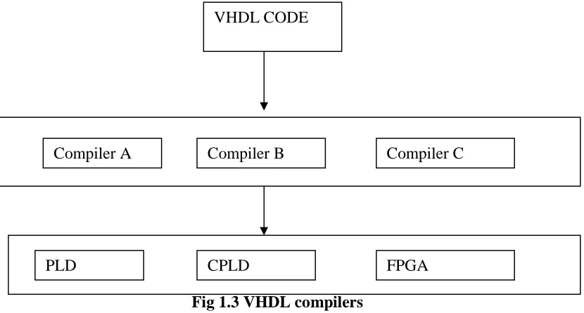
Fig 1.3 VHDL compilers VHDL CODE
Compiler A Compiler B Compiler C
1.3.5. BENCH MARKING CAPABILITIES:
Device independent design and portability allows benchmarking a design using different device architectures and different synthesis tools. We can take Device independent design and portability allows benchmarking a design a design description and synthesizing it, creating logic for it, evaluating the results and finally choosing the device, like a CPLD or an FPGA that best fits our design requirements.
1.3.6 ASIC MIGRATION:
The efficiency that VHDL generates allows our product to hit the market quickly if it has been synthesized on a CPLD or an FPGA. When production volume reaches appropriate levels, VHDL facilitates the development of Application Specific Integrated Circuits (ASIC). Sometimes, the exact code used with the PLD can be used with the ASIC and because VHDL is a well-defined language, we can be assured that out ASIC vender will deliver a device with expected functionality.
1.3.7 QUICK TIME TO MARKET AND LOW COST:
VHDL and programmable logic pair well together facilitate a speedy design process. VHDL permits designs to be described quickly. Programmable logic eliminates NRE expenses and facilitates quick design iterations. Synthesis makes it all possible. VHDL and programmable logic combine as a powerful vehicle to bring the product in market in record time.
1.3.8. DESIGN SYNTHESIS
The design process can be explained in six steps: Define the design requirements
Describe the design in VHDL Simulate the source code
Synthesize, Optimize, and Fit the design onto a suitable device. Simulate the post layout (fit) design model
1.3.9 DESCRIBE AND DESIGN REQUIREMENTS:
Before launching into writing code for our design, we must have a clear idea of design required setup and clock to output times, maximum frequency of operation and critical paths.
DESCRIBE THE DESIGN IN VHDL:
Formulate the design having an idea of design requirements, we have to write an efficient code that is realized through synthesis to the logic implementation we intended.
SIMULATE THE SOURCE CODE:
With source code simulation, flows can be detected early in the design cycle, allowing us to make correction with the least possible impact to the schedule. This is more efficient for larger designs, for which synthesis and place and route can take a couple of hours.
Fitter of Place & Route Routines
Post layout Simulation model (VHDL or other format)
Test bench or other stimulus
Report file: resource summary; static timing analysis
Device Programming file:
(for ex:JEDEC format)
Simulation software (VHDL or other simulator )
Waveform
1.3.10 SYNTHESIZE, OPTIMIZE AND FIT THE DESIGN: SYNTHESIS:
It is processes by which net lists or equations are created from design description, which may be abstracted VHDL synthesis software tools, convert VHDL descriptions to technology specific net lists or set of equations.
OPTIMIZATION:
The optimization process depends on three things. The form of the Boolean expressions, the type of resources available and automatic or user applied synthesis directives (sometimes called constraints). Optimization for CPLDs involves reducing the logic to a minimal sum of products, which is then further optimized for a minimal literal count. This reduces the product term utilization and number of logic block inputs required for any given expression.
1.3.11 SYNTHESIS PROCESS:
FITTING:
Fitting is the process of taking the logic produced by the synthesis and optimization process, and placing it into a logic devices, transforming the logic (if necessary) to obtain the best fit. It is a term typically used to describe the process of allocating resources for CPLD type architectures.
SIMULATE THE POST LAYOUT DESIGN MODEL:
A post layout simulation will enable us to verify not only the functionality of our design. But also the timing, such as set up, clock to output, and register-to-register times. If we are unable to meet our design objectives, then we need to either resynthesize, and/or fit our design to anew logic device.
PROGRAM THE DEVICE:
1.4. INTRODUCTION TO XILINX
The Xilinx ISE 9.1i provides Xilinx PLD designers with the basic design process using ISE 9.1i. In this chapter you will understand of how to create, verify, and implement a design.
This chapter contains the following sections: • “Getting Started”
• “Create a New Project” • “Create an HDL Source” • “Design Simulation”
• “Create Timing Constraints”
• “Implement Design and Verify Constraints” • “Re implement Design and Verify Pin Locations” • “Download Design to the Spartan™-3 Demo Board”
1.4.1 GETTING STARTED Software Requirements: - ISE 9.1i
Hardware Requirements: - Spartan-3 Start-up Kit, containing the Spartan-3 Start-up Kit Demo Board.
Starting the ISE Software
To start ISE, double-click the desktop icon,
Or start ISE from the Start menu by selecting: Desktop Icon
• Start
• All Programs • Xilinx ISE 9.1i • Project Navigator CREATE A NEW PROJECT
Create a new ISE project which will target the FPGA device on the Spartan-3 Start up Kit demo board.
1. Select File
New Project... The New Project Wizard appears. 2. Type tutorial in the Project Name field.
3. Enter or browse to a location (directory path) for the new project. A tutorial Subdirectory is created automatically.
4. Verify that HDL is selected from the Top-Level Source Type list. 5. Click Next to move to the device properties page
6. Fill in the properties in the table as shown below: • Product Category: All
• Family: Spartan3 • Device: XC3S200 • Package: FT256 • Speed Grade: -4
• Top-Level Source Type: HDL
• Synthesis Tool: XST (VHDL/Verilog) • Simulator: ISE Simulator (VHDL/Verilog) • Preferred Language: VHDL (or Verilog)
• Verify that Enable Enhanced Design Summary is selected.
Leave the default values in the remaining fields. When the table is complete, your project properties will look like the following:
Figure 1.5: Screenshot of Getting started to XILINK
1.4.2. CREATE AN HDL SOURCE
In this section, you will create the top-level HDL file for your design. Determine the language that you wish to use for the tutorial. Then, continue either to the “Creating a VHDL Source” section below, or skip to the “Creating a Verilog Source” section.
Create a VHDL source file for the project as follows: 1. Click the New Source button in the New Project Wizard. 2. Select VHDL Module as the source type.
3. Type in the file name counter.
4. Verify that the Add to project checkbox is selected. 5. Click Next.
6. Declare the ports for the counter design by filling in the port
7. Click Next, and then Finish in the New Source Wizard - Summary dialog box to complete the new source file template.
8. Click Next, then Next, then Finish. Next
2. Select the counter design source in the Sources window to display the related processes in the Processes window.
3. Click the “+” next to the Synthesize-XST process to expand the process group. 4. Double-click the Check Syntax process.
5. Close the HDL file.
1.4.3. DESIGN SIMULATION
VERIFYING FUNCTIONALITY USING BEHAVIOURAL SIMULATION
Create a test bench waveform containing input stimulus you can use to verify the functionality of the counter module. The test bench waveform is a graphical view of a test bench.
Create the test bench waveform as follows:
1. Select the counter HDL file in the Sources window.
2. Create a new test bench source by selecting Project New Source.
3. In the New Source Wizard, select Test Bench Waveform as the source type, and type counter_tbw in the File Name field.
4. Click Next.
5. The Associated Source page shows that you are associating the test bench waveform with the source file counter. Click Next.
6. The Summary page shows that the source will be added to the project, and it displays the source directory, type and name. Click Finish.
7. You need to set the clock frequency, setup time and output delay times in the Initialize Timing dialog box before the test bench waveform editing window opens.
Leave the default values in the remaining fields. 8. Click Finish to complete the timing initialization.
Figure 1.6: Initialize Timing
• Click on the blue cell at approximately the 300 ns to assert DIRECTION high so that the counter will count up.
• Click on the blue cell at approximately the 900 ns to assert DIRECTION low so that the counter will count down.
Figure 1.7: Test Bench Waveform 10. Save the waveform.
11. In the Sources window, select the Behavioural Simulation view to see that the test bench waveform file is automatically added to your project.
12. Close the test bench waveform.
1.4.4. SIMULATING DESIGN FUNCTIONALITY
Verify that the counter design functions as you expect by performing behaviour simulation as follows:
1. Verify that Behavioural Simulation and counter_tbw are selected in the Sources window.
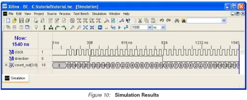
3. To view your simulation results, select the Simulation tab and zoom in on the transitions. The simulation waveform results will look like the following:
Figure 1.8: Simulation waveform
Note: You can ignore any rows that start with TX.
4. Verify that the counter is counting up and down as expected.
5. Close the simulation view. If you are prompted with the following message, “You have an active simulation open. Are you sure you want to close it? “, click yes to continue. You have now completed simulation of your design using the ISE Simulator.
1.4.5. CREATE TIMING CONSTRAINTS
Specify the timing between the FPGA and its surrounding logic as well as the frequency the design must operate at internal to the FPGA. The timing is specified by entering constraints that guide the placement and routing of the design. It is recommended that you enter global constraints. The clock period constraint specifies the clock frequency at which your design must operate inside the FPGA. The offset constraints specify when to expect valid data at the FPGA inputs and when valid data will be available at the FPGA outputs.
Entering Timing Constraints
To constrain the design do the following:
1. Select Synthesis/Implementation from the drop-down list in the Sources window. 2. Select the counter HDL source file.
3. Click the “+” sign next to the User Constraints processes group, and double-click the Create Timing Constraints process.ISE runs the Synthesis and Translate steps and automatically creates a User Constraints File (UCF). You will be prompted with the following message:
Note: You can also create a UCF file for your project by selecting Project Create New
Source.
In the next step, enter values in the fields associated with CLOCK in the Constraints Editor Global tab. 5. Select CLOCK in the Clock Net Name field, then select the Period toolbar button or double-click the empty Period field to display the Clock Period dialog box.
6. Enter 40 ns in the Time field.
1.4.6. IMPLEMENT DESIGN AND VERIFY CONSTRAINTS
Implement the design and verify that it meets the timing constraints specified in the previous section.
1. Select the counter source file in the Sources window.
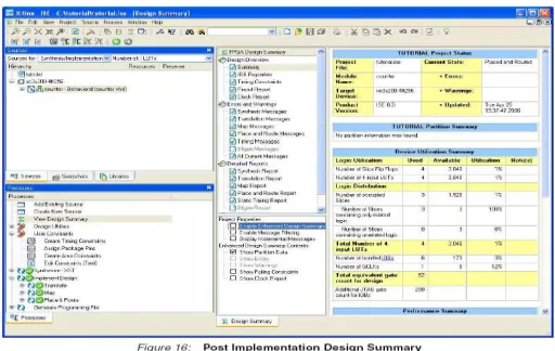
2. Open the Design Summary by double-clicking the View Design Summary process In the Processes tab.
3. Double-click the Implement Design process in the Processes tab.
4. Notice that after Implementation is complete, the Implementation processes have a green check mark next to them indicating that they completed successfully without Errors or Warnings.
Figure 1.9: Design Summary
5. Locate the Performance Summary table near the bottom of the design Summary.
6. Click the All Constraints Met link in the Timing Constraints field to view the Timing Constraints report. Verify that the design meets the specified timing requirements.
ASSIGNING PIN LOCATION CONSTRAINTS
To constrain the design ports to package pins, do the following: 1. Verify that counter is selected in the Sources window
2. Double-click the Assign Package Pins process found in the User constraints process group. The Xilinx Pin out and Area Constraints Editor (PACE) opens.
3. Select the Package View tab.
4. In the Design Object List window, enter a pin location for each pin in the Loc column using the following information:
5. Select File Save. You are prompted to select the bus delimiter type based on the synthesis tool you are using. Select XST Default <> and click OK.
6. Close PACE.
INTRODUCTION TO MLC NAND FLASH MEMORY LOSSLESS
COMPRESSION
2.1. INTRODUCTION
Introduction to memories: Definition and memory types: -
Electronic space provided by silicon chips (semiconductor memory chips) or magnetic/optical media as temporary or permanent storage for data and/or instructions to control a computer or execute one or more programs. Two main types of computer memory are: (1) Read only memory (ROM), smaller part of a computer's silicon (solid state) memory that is fixed in size and permanently stores manufacturer's instructions to run the computer when it is switched on. (2) Random access memory (RAM), larger part of a computer's memory comprising of hard disk, CD, DVD, floppies etc., (together called secondary storage) and employed in running programs and in archiving of data. Memory chips provide access to stored data or instructions that is hundreds of times faster than that provided by secondary storage.
Memory errors:
Memory errors are of two types, namely hard and soft.
ERROR CONTROL CODING:
Error detection and correction or error control are techniques that enable reliable delivery of digital data over unreliable communication channels(or storage medium.
Error detection is the detection of errors caused by noise or other impairments during transmission from the transmitter to the receiver.
Error correction is the detection of errors and reconstruction of the original, error-free data. The goal of error control coding is to encode information in such a way that even if the channel (or storage medium) introduces errors, the receiver can correct the errors and recover the original transmitted information.
ECC stands for "Error Correction Codes" [1] and is a method used to detect and correct errors introduced during storage or transmission of data. Certain kinds of RAM chips inside a computer implement this technique to correct data errors and are known as ECC Memory.
ECC Memory chips are predominantly used in servers rather than in client computers. Memory errors are proportional to the amount of RAM in a computer as well as the duration of operation. Since servers typically contain several Gigabytes of RAM and are in operation 24 hours a day, the likelihood of errors cropping up in their memory chips is comparatively high and hence they require ECC Memory.
Memory errors that are not corrected immediately can eventually crash a computer. This again has more relevance to a server than a client computer in an office or home environment. When a client crashes, it normally does not affect other computers even when it is connected to a network, but when a server crashes it brings the entire network down with it. Hence ECC memory is mandatory for servers but optional for clients unless they are used for mission critical applications.
Error-correcting codes are usually distinguished between convolutional codes and block codes: • Convolutional codes are processed on a bit-by-bit basis. They are particularly suitable for implementation in hardware, and the Viterbi decoder allows optimal decoding.
• Block codes are processed on a block-by-block basis. Early examples of block codes are repetition codes, Hamming codes and multidimensional parity-check codes. They were followed by a number of efficient codes, Reed-Solomon codes being the most notable due to their current widespread use. Turbo codes and low-density parity-check codes (LDPC) are relatively new constructions that can provide almost optimal efficiency.
Shannon's theorem is an important theorem in forward error correction, and describes the maximum information rate at which reliable communication is possible over a channel that has a certain error probability or signal-to-noise ratio (SNR). This strict upper limit is expressed in terms of the channel capacity. More specifically, the theorem says that there exist codes such that with increasing encoding length the probability of error on a discrete memory less channel can be made arbitrarily small, provided that the code rate is smaller than the channel capacity. The code rate is defined as the fraction k/n of k source symbols and n encoded symbols.
Some simple codes can detect but not correct errors; others can detect and correct one or more errors. This paper addresses one Hamming code that can correct a single-bit error and detect a double-bit error.
Parity Checking:
One simple way to detect errors is:
1. Count the number of ones in the binary message.
2. Append one more bit, called the parity bit, to the message
3. set the parity bit to either 0 or 1, so that the number of ones in the result is even. For example, if the original message contained 17 ones, the parity bit would be a one; if there had been 16 ones, the parity bit would be a zero.
4. Count the number of ones in the received message, including the parity bit. The result will always be even if no errors were encountered. (This approach also works if the parity bit is set to make the count come out odd, as long as the receiver checks for an odd count.)
Hamming Codes:
Hamming codes are an extension of this simple method that can used to detect and correct a larger set of errors[14]. Hamming’s development [Ham][12],[13] is a very direct construction of a code that permits correcting single-bit errors[7]. He assumes that the data to be transmitted consists of a certain number of information bits u, and he adds to these a number of check bits p such that if a block is received that has at most one bit in error, then p identifies the bit that is in error (which may be one of the check bits). Specifically, in Hamming’s code p is interpreted as an integer which is 0 if no error occurred, and otherwise is the 1-origined index of the bit that is in error. Let k be the number of information bits, and m the number of check bits used. Because the m check bits must check themselves as well as the information bits, the value of p, interpreted as an integer, must range from 0
to which is distinct values. Because m bits can distinguish cases, we must have (1)
This is known as the Hamming rule. It applies to any single error correcting (SEC) binary FEC block code in which all of the transmitted bits must be checked. The check bits will be interspersed among the information bits in a manner described below. Because p indexes the bit (if any) that is in error, the least significant bit of p must be 1 if the erroneous bit is in an odd position, and 0 if it is in an even position or if there is no error. A simple way to achieve this is to let the least significant bit of p, , be an even parity check on the odd positions of the block, and to put in an odd position. The receiver then checks the parity of the odd positions (including that of ). If the result is 1, an error has occurred in an odd position, and if the result is 0, either no error occurred or an error occurred in an even position. This satisfies the condition that p should be the index of the erroneous bit, or be 0 if no error occurred.
Putting the check bits in power-of-two positions (1, 2, 4, 8, …) has the advantage that they are independent. That is, the sender can compute independently of , , … and, more generally, it can compute each check bit independently of the others.
As an example, let us develop a single error correcting code for Solving (1) for m=3 gives with equality holding. This means that all possible values of the m check bits are used, so it is particularly efficient. A code with this property is called a perfect code.1
This code is called the (7, 4) Hamming code, which signifies that the code
length is 7 and the number of information bits is 4. The positions of the check bits and the information bits are shown below.
1 2 3 4 5 6 7
Reed-Solomon codes:
Reed-Solomon codes were developed in 1960 by Irving S. Reed and Gustave Solomon, who were then members of MIT Lincoln Laboratory. Their seminal article was entitled "Polynomial Codes over Certain Finite Fields." (Reed & Solomon 1960) When the article was written, an efficient decoding algorithm was not known [17,18]. A solution for the latter was found in 1969 by Elwyn Berlekamp and James Massey, and is since known as the Berlekamp-Massey decoding algorithm. In 1977, RS codes were notably implemented in the Voyager program in the form of concatenated codes. The first commercial application in mass-produced consumer products appeared in 1982 with the compact disc, where two interleaved RS codes are used.
The parameters of a Reed-Solomon code are: m = the number of bits per symbol
n = the block length in symbols
k = the uncoded message length in symbols (n-k) = the parity check symbols (check bytes) t = the number of correctable symbol errors (n-k)=2t (for n-k even)
(n-k)-1 = 2t (for n-k odd)
of the transmitted message is redundant data. In general, due to decoder constraints, the block length cannot be arbitrarily large.
The block length for the PerFEC codes is bounded by the following equation:
The number of correctable symbol errors (t), and block length (n) is set by the user.
RS codes are widely implemented in digital storage devices and digital communication standards, though they are being slowly replaced by more modern low-density parity-check (LDPC) codes or turbo codes. For example, RS codes are used in the digital video broadcasting (DVB) standard DVB-S, but LDPC codes are used in its successor DVB-S2.
The encoders and decoders for Hamming and Hsiao codes, for example, have low encoding and decoding complexity, but also have relatively low error- correcting capacity (e.g., Hamming is single error-correcting, double error-detecting). To achieve higher error- correcting capability, codes like Reed Solomon[11] or BCH require more sophisticated decoding algorithms.
LDPC CODES:
LOW-density parity-check (LDPC) codes were first discovered by Gallager in the early 1960s [2] and have recently been rediscovered and generalized .It has been shown that these codes achieve a remarkable performance with iterative decoding that is very close to the Shannon limit[3]. Consequently, these codes have become strong competitors to turbo codes for error control in many communication and digital storage systems where high reliability is required.
applications like optical communications that require very fast encoders and decoders and very low bit error-rates.
Memory cells have been protected from soft errors for more than a decade; due to the increase in soft error rate in logic circuits, the encoder and decoder circuitry around the memory blocks have become susceptible to soft errors as well and must also be protected. We introduce a new approach to design fault-secure encoder and decoder circuitry for memory designs.
Hamming codes are often used in today’s memory systems to correct single error and detect double errors in any memory word. In these memory architectures, only errors in the memory words are tolerated and there is no preparation to tolerate errors in the supporting logic (i.e. encoder and corrector).
However combinational logic has already started showing susceptibility to soft errors, and therefore the encoder and decoder (corrector) units will no longer be immune from the transient faults. Therefore, protecting the memory system support logic implementation is more important. Here we proposed a lossless system which detect the errors and correct the errors on 32bit input at a time to maintain the 32 bit processor with error free. Generally the errors occur in the memory is due to redundancy information .So if we remove the redundancy obviously the error prone will be reduced. In this project based on the proposed technique error free data oriented architecture is developed to encode and to decode the information.
Each Data compressor can process four bytes of data into and from a block of data every clock cycle. The data entering the system needs to be clocked in at a rate of 4n bytes every clock cycle, where n is the number of compressors in the system. This is to ensure that adequate data is present for all compressors to process rather than being in an idle state.
2.2. GOAL OF THE THESIS:
To achieve higher compression rates using 32 bit compression /decompression architecture with least increase in latency to reduce the errors due to introduction of redundancy information.
2.3. LITERATURE SURVEY:
2.3.1. COMPRESSION TECHNIQUES:
At present there is an insatiable demand for ever-greater bandwidth in communication networks and forever-greater storage capacity in computer system. This led to the need for an efficient compression technique. The compression is the process that is required either to reduce the volume of information to be transmitted – text, fax and images or reduce the bandwidth that is required for its transmission – speech, audio and video. The compression technique is first applied to the source information prior to its transmission.
Compression algorithms can be classified in to two types, namely Lossless Compression
Lossy Compression
2.3.1.1. LOSSLESS COMPRESSION:
In this type of lossless compression algorithm, the aim is to reduce the amount of source information to be transmitted in such a way that, when the compressed information is decompressed, there is no loss of information. Lossless compression is said, therefore, to be reversible. i.e., Data is not altered or lost in the process of compression or decompression. Decompression generates an exact replica of the original object. The Various lossless Compression Techniques are,
• Lempel-Ziv and Welch algorithm LZW • Huffman
Example applications of lossless compression are transferring data over a network as a text file since, in such applications, it is normally imperative that no part of the source information is lost during either the compression or decompression operations and file storage systems (tapes, hard disk drives, solid state storage, file servers) and communication networks (LAN, WAN, wireless).
2.3.1.2. LOSSY COMPRESSION:
The aim of the Lossy compression algorithms is normally not to reproduce an exact copy of the source information after decompression but rather a version of it that is perceived by the recipient as a true copy.
The Lossy compression algorithms are:
• JPEG (Joint Photographic Expert Group) • MPEG (Moving Picture Experts Group) • CCITT H.261 (Px64)
Example applications of lossy compression are the transfer of digitized images and audio and video streams. In such cases, the sensitivity of the human eye or ear is such that any fine details that may be missing from the original source signal after decompression are not detectable.
2.3.1.3. TEXT COMPRESSION:
There are three different types of text – unformatted, formatted and hypertext and all are represented as strings of characters selected from a defined set. The compression algorithm associated with text must be lossless since the loss of just a single character could modify the meaning of a complete string. The text compression is restricted to the use of entropy encoding and in practice, statistical encoding methods.
There are two types of statistical encoding methods which are used with text: one which uses single character as the basis of deriving an optimum set of code words and the other which uses variable length strings of characters. Two examples of the former are the Huffman and Arithmetic coding algorithms and an example of the latter is Lempel-Ziv (LZ) algorithm.
2.3.2. PREVIOUS WORK ON LOSSLESS COMPRESSION METHODS:
A second Lempel-Ziv method used a content addressable memory (CAM) capable of performing a complete dictionary search in one clock cycle. The search for the most common string in the dictionary (normally, the most computationally expensive operation in the Lempel-Ziv algorithm) can be performed by the CAM in a single clock cycle, while the systolic array method uses a much slower deep pipelining technique to implement its dictionary search. However, compared to the CAM solution, the systolic array method has advantages in terms of reduced hardware costs and lower power consumption, which may be more important criteria in some situations than having faster dictionary searching. In the authors show that hardware main memory data compression is both feasible and worthwhile. The authors also describe the design and implementation of a novel compression method, the XMatchPro algorithm. Its exhibit the substantial impact such memory compression has on overall system performance.
The adaptation of compression code for parallel implementation is investigated by Jiang and Jones. They recommended the use of a processing array arranged in a tree-like structure. Although compression can be implemented in this manner, the implementation of the decompressor’s search and decode stages in parallel hardware would greatly increase the complexity of the design and it is likely that these aspects would need to be implemented sequentially. An FPGA implementation of a parallel binary arithmetic coding architecture that is able to process 8 bits per clock cycle compared to the standard 1 bit per cycle is described by Stefoetal. Although little research has been performed on architectures involving several independent compression units working in a concurrent cooperative manner, IBM has introduced the MXT chip, which has four independent compression engines operating on a shared memory area. The four Lempel-Ziv compression engines are used to provide data throughput sufficient for memory compression in computer servers.
2.3.2.1. STATISTICAL METHODS: Statistical Modeling of lossless data compression system is based on assigning values to events depending on their probability. The higher the value, the higher the probability. The accuracy with which this frequency distribution reflects reality determines the efficiency of the model. In Markov modeling, predictions are done based on the symbols that precede the current symbol.
2.3.2.2. DICTIONARY METHODS:
Dictionary Methods try to replace a symbol or group of symbols by a dictionary location code. Some dictionary-based techniques use simple uniform binary codes to process the information supplied. Both software and hardware based dictionary models achieve good throughput and competitive compression. The UNIX utility ‘compress’ uses Lempel-Ziv-2 (LZ2) algorithm and the data compression Lempel-Ziv (DCLZ) family of compressors initially invented by Hewlett- Packard[16] and currently being developed by AHA[17],[18] . It uses a tag attached to each dictionary location to identify which node should be eliminated once the dictionary becomes full.
2.4. XMATCHPRO BASED SYSTEM:
The Lossless data compression system is derivative of the XMatchPro Algorithm of the previous methods are overcome by using the XmatchPro algorithm in design. The objective is then to obtain better compression ratios and still maintain a high throughput so that the compression/decompression processes do not slow the original system down. The flexibility provided by using this technology is of great interest since the chip can be adapted to the requirements of a particular application easily.
FUNCTIONS OF LOSSLESS COMPRESSION
3.1. BASICS OF COMMUNICATION:
Lossless compression removes redundant information from the data while they are being transmitted or before they are stored in memory, and lossless decompression reintroduces the redundant information to recover fully the original data. In the same way, the data is compressed before it is stored and decompressed when it is retrieved, thus increasing the effective capacity of the storage device.
3.2. PROPOSED METHOD:
In it discusses about the Parallel Algorithm that can be implemented for High Speed Data Compression. The authors gives the basic idea about how the Data Compression is carried out using the Lempel-Ziv Algorithm and how it could be altered for Parallelism of the algorithm. It describes the Lempel-Ziv algorithm as a very efficient universal data compression technique, based upon an incremental parsing technique, which maintains codebooks of parsed phrases at the transmitter and at the receiver. An important feature of the algorithm is that it is not necessary to determine a model of the source.
3.3. BACKGROUND:
It discusses about the parallelism in Data Compression Techniques and the authors explain the Parallel Architecture for High Speed Data Compression. In this paper, it expresses Data Communication as an essential component of high-speed data communication and storage.
It discusses about the various methods of Data Compression and their Techniques and drawbacks and proposes a new methodology for a high speed Parallel Lossless Data Compression. The authors describes the research and hardware implementation of a high performance parallel multi compressor chip which could able to meet the intensive data processing demands of highly concurrent system. The authors also investigate the performance of alternative input and output routing strategies for realistic data sets demonstrate that the design of parallel compression devices involves important tradeoffs that affect compression performance, latency and throughput. Compression ratio achieved by the proposed universal code uniformly approaches the lower bounds on the compression ratios attainable by block-to-variable codes and variable-to-block codes designed to match a completely specified source.
3.4. USAGE OF XMATCHPRO ALGORITHM:
The Lossless Parallel Data Compression system designed uses the XMatchPro Algorithm. The XMatchPro algorithm uses a fixed-width dictionary of previously seen data and attempts to match the current data element with a match in the dictionary. It works by taking a 4-byte word and trying to match or partially match this word with past data. This past data is stored in a dictionary, which is constructed from a content addressable memory.
As each entry is 4 bytes wide, several types of matches are possible. If all the bytes do not match with any data present in the dictionary they are transmitted with an additional miss bit. If all the bytes are matched then the match location and match type is coded and transmitted, this match is then moved to the front of the dictionary.
2). Match type: Indicates which bytes of the incoming tuple have matched. 3). Characters that did not match transmitted in literal form.
With the increase in silicon densities, it is becoming feasible for multiple XMatchPros to be implemented in parallel onto a single chip. A parallel system with distributed memory architecture is based on having multiple data compression and decompression engines working independently on different data at the same time.
A description of the XMatchPro algorithm in pseudo-code is given in the below. Clear the dictionary;
Set the next free location (NFL) to 0; Do
{
read in a tuple T from the data stream; search the dictionary for tuple T; IF (full or partial hit)
{
determine the best match location ML and match type MT; output ‘0’;
output any required literal characters of T; }
ELSE { output ‘1’; output tuple T; }
IF (full hit) {
move dictionary entries 0 to ML -1 down by one location; }
ELSE {
}
copy tuple T to dictionary location 0; }
WHILE (more data is to be compressed);
PSEUDO CODE FOR XMATCHPRO ALGORITHM
This data is stored in memory distributed to each processor. There are several approaches in which data can be routed to and from the compressors that will affect the speed, compression and complexity of the system. Lossless compression removes redundant information from the data while they are transmitted or before they are stored in memory. Lossless decompression reintroduces the redundant information to recover fully the original data. There are two important contributions made by the current parallel compression & decompression work, namely, improved compression rates and the inherent scalability.
Significant improvements in data compression rates have been achieved by sharing the computational requirement between compressors without significantly compromising the contribution made by individual compressors. The scalability feature permits future bandwidth or storage demands to be met by adding additional compression engines.
3.4.1. THE XMATCHPRO BASED COMPRESSION SYSTEM:
Previous research on the lossless XMatchPro data compressor has been on optimizing and implementing the XMatchPro algorithm for speed, complexity and compression in hardware. The XMatchPro algorithm uses a fixed width dictionary of previously seen data and attempts to match the current data element with a match in the dictionary. It works by taking a 4-byte word and trying to match this word with past data. This past data is stored in a dictionary, which is constructed from a content addressable memory.
compression performance. Since the number of bits needed to code each location address is a function of the dictionary size greater compression is obtained in comparison to the case where a fixed size dictionary uses fixed address codes for a partially full dictionary. In the parallel XMatchPro system, the data stream to be compressed enters the compression system, which is then partitioned and routed to the compressors.
For parallel compression systems, it is important to ensure all compressors are supplied with sufficient data by managing the supply so that neither stall conditions nor data overflow occurs.
3.4.2. THE MAIN COMPONENT- CONTENT ADDRESSABLE MEMORY:
Dictionary based schemes copy repetitive or redundant data into a lookup table (such as CAM) and output the dictionary address as a code to replace the data. The compression architecture is based around a block of CAM to realize the dictionary. This is necessary since the search operation must be done in parallel in all the entries in the dictionary to allow high and data-independent throughput.
The number of bits in a CAM word is usually large, with existing implementations ranging from 36 to 144 bits. A typical CAM employs a table size ranging between a few hundred entries to 32K entries, corresponding to an address space ranging from 7 bits to 15 bits. The length of the CAM varies with three possible values of 16, 32 or 64 tuples trading complexity for compression. The no. of tuples present in the dictionary has an important effect on compression.
In principle, the larger the dictionary the higher the probability of having a match and improving compression. On the other hand, a bigger dictionary uses more bits to code its locations degrading compression when processing small data blocks that only use a fraction of the dictionary length available. The width of the CAM is fixed with 4bytes/word Content Addressable Memory (CAM) compares input search data against a table of stored data, and returns the address of the matching data. CAMs have a single clock cycle throughput making them faster than other hardware and software-based search systems. The input to the system is the search word that is broadcast onto the searchlines to the table of stored data. Each stored word has a matchline that indicates whether the search word and stored word are identical (the match case) or are different (a mismatch case, or match).
expected. The overall function of a CAM is to take a search word and return the matching memory location.
3.4.2.1. MANAGING DICTIONARY ENTRIES:
Since the initialization of a compression CAM sets all words to zero, a possible input word formed by zeros will generate multiple full matches in different locations. The Xmatchpro compression system simply selects the full match closer to the top. This operational mode initializes the dictionary to a state where all the words with location address bigger than zero are declared invalid without the need for extra logic. The reason is that location x can never generate a match until the data contents of location x-1 are different from zero because locations closer to the top have higher priority generating matches. Also to increase dictionary efficiency, only one dictionary position contains repeated information and in the best case.
4.1. IMPLEMENTATION OF XMATCHPRO BASED COMPRESSOR
4.2. DESCRIPTION OF LANGUAGE USED IN SOURCE CODE:
Array is of length of 64X32 bit locations. This is used to store the unmatched incoming data and when a new data comes, the incoming data is compared with all the data stored in this array. If a match occurs, the corresponding match location is sent as output else the incoming data is stored in next free location of the array & is sent as output. The last component is the cam comparator and is used to send the match location of the CAM dictionary as output if a match has occurred. This is done by getting match information as input from the comparator.
Suppose the output of the comparator goes high for any input, the match is found and the corresponding address is retrieved and sent as output along with one bit to indicate that match is found. At the same time, suppose no match occurs, or no matched data is found, the incoming data is stored in the array and it is sent as the output. These are the functions of the three components of the Compressor. The hardware descriptions of these modules are done using VHDL Language. VHDL is an acronym for Very high-speed integrated circuits Hardware Description Language. It can be used to model a digital system at many levels of the abstraction, ranging from the algorithmic level to gate level.
The VHDL language can be regarded as an integrated amalgamation of the following languages: Sequential language
Concurrent language Net-list language Timing specifications
Waveform generation language.
So the language has constructs that enable you to express the concurrent or sequential behavior of a digital system with or without timing. It also allows modeling the system as an inter-connection of components.
4.3. DESIGN OF COMPRESSOR / DECOMPRESSOR:
The block diagram gives the details about the components of a single 32- bit compressor / decompressor. The Same design approach is used for designing a 64-bit Compression/Decompression system which is essentially used for comparison of increased compression rates given by the 64-bit Lossless Parallel High-Speed Data Compression System. There are three components namely
decompressor control.
The compressor has the following components comparator
array
cam comparator.
The last component is the Cam comparator and is used to send the incoming data and all the stored data in array one by one to the comparator. Suppose output of comparator goes high for any input, then the match is found and the corresponding address (match based compressor).
At the same time, suppose no match is found, then the incoming data stored in the array is sent as output. These are the functions of Array, so it stores the data in the Array and if the match hit data is 1, it indicates the data is present in the Array, then it instructs to find the data from the Array with the help of the address input and sends as output to the data out location) is retrieved and sent as output along with the three components of the XMatchPro.
. The decompressor has the following components – Array and Processing Unit. Array has the same function as that of the array unit used in the Compressor. It is also of the same length. Processing unit checks the incoming match hit data and if it is 0, it indicates that the data is not present in the one bit to indicate the match is found.
The Control has the input bit called C / D i.e., Compression / Decompression indicates whether compression or decompression has to be done. If it has the value 0 then compressor is stared when the value is 1 decompression is done.
SIMULATION RESULTS
5.1 SIMULATION RESULT:
The design coded in VHDL is simulated using Xilinx The obtained waveforms are as follows
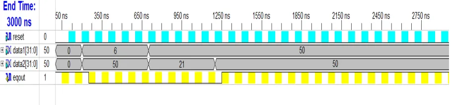
COMPARATOR:
Values of Data 1 and Data 2 are forced. Now value of reset is forced to 1. The output eqout is zero.
Now value of reset is forced to 0.
And if Data 1 and Data 2 are equal then eqout value is 1. If Data 1 and Data 2 are not equal value of eqout is 0.
CAM COMPARATOR:
Fig 5.2 Cam Comparator output waveform
1. Value of reset is forced to 1.Then match hit value is zero and address out is also zero.
3. Now if any value of h0 to h32 does not match with any in array then we get value of match hit as zero.
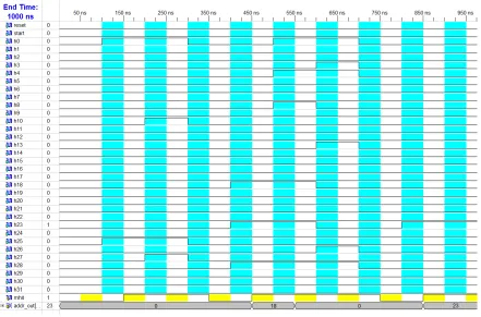
CAM:
Fig.5.3 Content Addressable Memory output waveform
1. Value of reset is forced to 1.Then match hit value is zero and address out is also zero.
2. Then now value if start is forced to 0 and now if the data entered in any one of the value from h0 to h63 is entered then we get the match hit value 1 and now address location of that bit that is already present in array.
3. Now if any value of h0 to h63 does not match with any in array then we get value of match hit as zero.
DATA COMPRESSION:
Fig: The RTL Schematic for vhdl codes are generated using Xilinx
Fig. 5.4 32-bit Single Compression output waveform
Now value of data is entered and if datain is equal to dataout matchhit is 1. If not, its value is zero.
DE-COMPRESSION
:
Fig: The RTL Schematic for vhdl codes are generated using Xilinx
5.2 Xilinx synthesis results for target device xc2v1500bg575-6: 5.2.1. 32-bit Single Compression System:
======================================================== *Synthesis Options Summary * ========================================================
---- Source Parameters
Input File Name: "xmatchpro.prj"
Input Format : mixed
Ignore Synthesis Constraint File: NO ---- Target Parameters
Output File Name: "xmatchpro" Output Format: NGC
Target Device: xc2v1500-6-bg575
===================================================== * HDL Compilation *
=====================================================
Compiling vhdl file "E:/proj/xilinx/s_comp32/s_comp32/comparator.vhd" in Library work. Architecture arch_comp of Entity comparator is up to date.
Compiling vhdl file "E:/proj/xilinx/s_comp32/s_comp32/camcomp.vhd" in Library work. Architecture arch_cam32 of Entity camcomp is up to date.
Compiling vhdl file "E:/proj/xilinx/s_comp32/s_comp32/cam.vhd" in Library work. Architecture arch_xmatch of Entity xmatchpro is up to date.
Applications
6. APPLICATIONS:
For visual and audio data, some loss of quality can be tolerated without losing the essential nature of the data. By taking advantage of the limitations of the human sensory system, a great deal of space can be saved while producing an output which is nearly in distinguishable from original.
Lossy image compression is used in digital cameras, greatly increasing their storage capacities while hardly degrading picture quality at all. Similarly, DVDs use the lossy MPEG-2 codec for video compression.
In lossy audio compression, methods of psychoacoustics are used to remove non-audible (or less audible) components of the signal. Compression of human speech is often performed with even more specialized techniques, so that "speech compression" or "voice coding" is sometimes distinguished as a separate discipline than "audio compression". Different audio and speech compression standards are listed under audio codecs. Voice compression is used in Internet telephony for example, while audio compression is used for CD ripping and is decoded by MP3 players.
CONCLUSION:
In this project we presented a method to implement lossless data compression system which operates at high-speed to achieve high compression rate. By using architecture of compressors, the data compression rates are significantly improved and also inherent scalability of parallel architecture is possible.
The algorithm “XMATCHPRO merge” used in this project is efficient at compressing and the flexibility provided by using this technology is of great interest, since the chip can be adapted to the requirements of a particular application easily.So by this the error prone in the memory is reduced drastically.
References: