Low-Power Adder Design Using Full-Swing
Gate Diffusion Input Logic
N.Nagaraju
1, A.Gowri
2,M.Gowthami
3, Dr.S.
M.Ramesh
4Assistant Professor, Dept. of ECE, Adhiyamaan Engineering College, Hosur, Tamilnadu, India 1
UG Scholar, Dept. of ECE, Adhiyamaan Engineering College, Hosur, Tamilnadu, India 2,3
Associate Professor, Dept. of ECE, Bannari amman institute of technology, Sathyamangalam, Tamilnadu, India4
ABSTRACT: Nowadays for each and every designing in VLSI era the power consumption plays a vital role. Low power has emerged as a principal theme in today‟s electronics industry. The need for low power has caused a major paradigm shift where power dissipation has become important consideration as performance and area. The low power VLSI design has important role in designing of many electronic design systems. On designing any combinational or sequential circuits, the power consumption, implementation area, voltage leakage and efficiency of the circuit are the important parameters to be considered initially. In designing of high speed adder, subtractor and multipliers are constructed basically with the adders. So speeding up the adder efficiency is important to all the processors. One of the basic adder is the carry look ahead adder. An adder can be designed by the full swing gate diffusion input technology. On comparing to the design of adders like ripple carry adder, carry look ahead adder etc., using conventional CMOS technology, the full swing gate diffusion input technology method is efficiently used. Full swing gate diffusion input is a new technique of low power digital combinational circuit. The name full swing denotes the high speed of operation. This technique allows reducing power consumption, propagation delay, and area of digital circuits while maintaining low complexity of logic design. This method is suitable for design of fast, low-power circuits using a reduced number of transistors.
KEYWORDS: Low power, GDI,CMOS,Tanner EDA.
I.INTRODUCTION
Nowadays the research centres are mainly concerned with the low power VLSI technology where it has been playing an important role in the industrial era. The growing market of portable (e.g., cellular phones, gaming consoles, etc.), battery-powered electronic systems demands microelectronic circuits design with ultra low power dissipation. As the integration, size, and complexity of the chips continue to increase, the difficulty in providing adequate cooling might either add significant cost or limit the functionality of the computing systems which make use of those integrated circuits. As the technology node scales down to 65nm there is not much increase in dynamic power dissipation. However the static or leakage power is same as or exceeds the dynamic power beyond 65nm technology node. Hence the technique to reduce power dissipation is not limited to dynamic power. In this article we discuss circuit and logic design approaches to minimize Dynamic, Leakage and Short Circuit power dissipation. Power optimization in a processor can be achieved at various abstract levels. System/Algorithm/Architecture have a large potential for power saving even these techniques tend to saturate as we integrate more functionality on an IC. So optimization at Circuit and Technology level is also very important for miniaturization of ICs. Total Power dissipated in a CMOS circuit is sum total of dynamic power, short circuit power and static or leakage power. Design for low-power implies the ability to reduce all three components of power consumption in CMOS circuits during the development of a low power electronic products.
II.PROPOSED MODEL AND ITS MERITS
transistors (as compared to CMOS design and pass transistor logic), while improving logic level swing and static power characteristics and allowing simple top-down design by using small cell library.
A ripple carry adder is a logic circuit in which the carry-out of each full adder is the carry in of the succeeding next most significant full adder. It is called a ripple carry adder because each carry bit gets rippled into the next stage. In a ripple carry adder the sum and carry out bits of any half adder stage is not valid until the carry in of that stage occurs. Propagation delays inside the logic circuitry are the reason behind this. Propagation delay is time elapsed between the application of an input and occurrence of the corresponding output.
The basic GDI cell can perform six operations by using two transistors.
Table: Various logic functions of GDI for different input configurations
a) WORKING OF GDI CELL:
MUX design is the most complex design that can be implemented. with GDI, which requires only two transistors, which requires 8-12 transistors with standard CMOS design.
The operation of GDI cell is as follows, when the power supply and the ground is given to the substrates of PMOS and NMOS transistors, the GDI cell is in ON condition. So that we can give the inputs accordingly.
When the input is given as A to the common gate terminal, B to the source of the PMOS and logic 0 to the
drain of the NMOS, the NMOS transistor will be in cut off stage. The input from the common gate gets inverted at the PMOS side and the result at the output side will be A‟B which gives the function F1.
Likewise when the inputs are given as A, „1‟ and B to the common gate, source of PMOS and drain of
NMOS, both the transistors will be in ON condition and the output will be given as A‟+B which gives the function F2.
When the gate terminal is given as A , PMOS is given as B and NMOS is given as logic 1 then both the transistors will be in ON condition and it will perform the logical OR operation.
If PMOS input is given as logic 0 then it will be in cut off stage. When we give the input for gate as A and the
NMOS input as B, it will perform the logical AND operation.
And finally when the source and drain of the PMOS and NMOS transistors are given as logic 1 and logic 0 correspondingly and the gate terminal is given a input, then the PMOS will be in ON condition and the NMOS will be in OFF condition. So at the output side we get the inverted output. So we get the NOT operation.
III.METHODOLOGY
Gate Diffusion Input(GDI) design technique was introduced as a promising alternative to complementary CMOS Logic design. Originally proposed for fabrication in Silicon on Insulator (SOI) and twin-well CMOS processes. GDI methodology allow implementation of a wide range of complex logic functions using only two transistors. It was shown that area and dynamic power of GDI combinatorial and sequential logic were significantly reduced, as compared to standard CMOS implementations.
One of the inputs are directly diffused into the gates of the transistors of N-type and P-type devices. Gate Diffusion Input technique reduces power dissipation, propagation delay, and area of digital circuits.
1) Gate Diffusion Input (GDI CELL) contains three inputs –G (common gate input of NMOS and PMOS), P(input to the source/drain of PMOS), and N (input to the source/drain of NMOS).
2) The source of PMOS in a GDI cell is not connected to VDD and source of NMOS is not connected to GND. This feature gives GDI cell two extra input pins for use which makes GDI design more flexible.
3) Bulks of both NMOS and PMOS are connected to N or P (respectively), so it can be arbitrarily biased at contrast with CMOS inverter.
A simple change of the input configuration of the simple GDI cell corresponds to very different Boolean functions. Most of these functions require a complex (6-12 transistors) gate in CMOS (as well as in standard PTL implementations), but are very simple (only two transistors per function) in the GDI design methodology. GDI enables simpler gates, lower transistor count, and lower power dissipation.
Our technology provides logical building blocks that enable complex functions using fewer components than current methods. The implementation is simple, allowing for smaller die size and less expensive solutions. The technology is based on standard CMOS fabrication methods and can be simulated by automatic design tools. Our technology basic cell consists of only two transistors with four terminals: three inputs being common gate and source\drain of each transistor, and a common output.
With this configuration one can implement all standard CMOS logic gates – with fewer components. Several complex functions, such as MUX, are implemented in a single cell (such functions would take no less than six components in standard CMOS design). The use of significantly reduced number of components allows for smaller die size and
significant reduction of power consumption. This basic GDI cell has a wide range of application areas such as Digital
Electronic Communication, wireless chip design, consumer electronic, VLSI systems, Board Design, ASIC, micro-processors
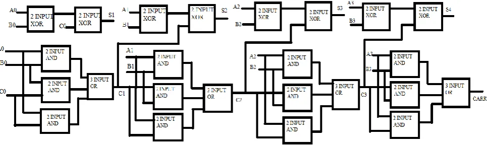
IV. BLOCK DIAGRAM OF 4 BIT RIPPLE CARRY ADDER
Fig: 4 bit ripple carry adder
Table for the three input and the corresponding output SUM and CARRY. The Boolean Expression describing the binary adder circuit is then deduced.
The above shown figure is the 4 bit ripple carry adder. It can be constructed by cascading full adder blocks in series. One full adder is responsible for the addition of two binary digits at any stage of ripple carry. The carry out of one stage is fed directly to the carry-in of the next stage. This type of circuits provides lower power consumption as well as compact layout giving smaller chip area.[3]
By using this technology we can implement a large circuit into a smaller chip. So that, this technology may improve the efficiency of the circuit design. In a ripple carry adder the sum and carry out bits of any half adder stage is not valid until the carry in of that stage occurs. Propagation delays inside the logic circuitry are the reason behind this. Propagation delay is time elapsed between the application of an input and occurance of the corresponding output.
V. RESULT AND DISCUSSION
a) GDI AND GATE
Schematic diagram of GDI AND gate
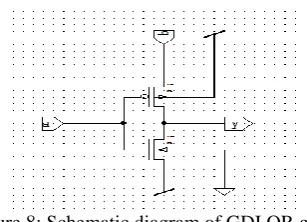
One of the input is given to the common gate terminals of both the transistors (PMOS and NMOS). And another input is given to the source of NMOS transistor. The substrate of PMOS is given to the power supply and the substrate of NMOS is given to ground. The simulation result is given below.
b) GDI OR GATE
Figure 8: Schematic diagram of GDI OR gate
c) GDI EX-OR GATE
Figure 11: Schematic diagram of GDI EX-OR gate
The EX-OR operation is carried out by using only 4 transistors in the GDI technique. The simplicity of the circuit helps us to improve the efficiency of the overall design. In this method two transistors are used to get the inverted output of one input and another two transistors are used to perform the EX-OR operation.
The main advantage of the GDI cell is that, it has three input terminals. So the inverted output of one input is fed as an input to the drain terminal of NMOS transistor in another GDI cell and another input is fed to the common gate terminal of the second GDI cell. As we are giving the power supply and ground to both the GDI cells we can get the output at the second GDI cell.
d) GDI FULL ADDER
Figure 14: Symbol mode representation of GDI full adder
The proposed full adder circuit is shown in fig14. One important requirement of full adder cells especially at low voltage is to provide enough driving power to the following circuits. The drivability is ensured by the full signal swing and decoupling of inputs and outputs (at least one inverter per cell) so that the adder cell can be cascaded arbitrarily and work reliably in any circuit configuration. So the second stage of full adder cells which generate Sum
and Carrymust have enough drivability.
e) 4 BIT GDI RIPPLE CARRY ADDER
Figure 16: Symbol mode representation of 4 bit ripple carry adder
The above shown figure is the 4 bit ripple carry adder. It can be constructed by cascading full adder blocks in series. One full adder is responsible for the addition of two binary digits at any stage of ripple carry. The carry out of one stage is fed directly to the carry-in of the next stage. This type of circuits provides lower power consumption as well as compact layout giving smaller chip area.[3]
By using this technology we can implement a large circuit into a smaller chip. So that, this technology may improve the efficiency of the circuit design. In a ripple carry adder the sum and carry out bits of any half adder stage is not valid until the carry in of that stage occurs. Propagation delays inside the logic circuitry are the reason behind this. Propagation delay is time elapsed between the application of an input and occurance of the corresponding output. The various parameters of 4 bit, 8 bit and 16 bit ripple carry adders are shown below.
Adder CMOS design GDI design 4 bit ripple
carry adder
8 bit ripple carry adder
16 bit ripple carry adder
4 bit ripple carry adder
8 bit ripple carry adder
16 bit ripple carry adder
No. of transistors
200 400 800 72 144 216
delay 3.69 s 7.93 s 17.82 s 0.95 s 1.98 s 3.34 s
Average power consumed
4.67 e5 watts 9.89 e5 watts 17.15 e5
watts
1.00 e5watts 2.08e5 watts 4.82 e5 watts
VI. CONCLUSION
Here we have designed the basic gates, full adder and the ripple carry adder using both conventional CMOS design and GDI technique and comparison results were analysed. By implementing this technique in real time applications, we can reduce the die area by reducing the transistor count. So the average power consumption and the execution time of the circuit are also reduced.
REFERENCES
1. Arkadiy morgenshtein, Alexander fish, Viacheslav yuzhaninov and Alexey kovshilovsky “Full swing Gate Diffusion Input Logic- Case study of low power CLA adder design” in Faculty of Engineering, Bar- Ilan university, Ramat-can 52900, Israel. INTEGRATION,theVLSI journal year 2014, PP 62–70
3. D. Markovic, B. Nikolic and V.G. Oklobdzija “A general method in synthesis of pass-transistor circuits” Microelectronics Journal 31 (2000), 991–998.
4. Arkadiy morgenshtein, Alexander fish and Israel A. Wagner “Gate diffusion input – a novel power efficient method for digital circuits: a design methodology” in IBM research Laboratory, Haifa, Israel, e-mail: [email protected] .
5. Pooja Verma1and Rachna Manchanda “Review Of Various GDI Techniques For Low Power Digital Circuits” in research scholar, chandigar engineering college, Landran (Mohali).