Article
Slope Compensation Design for a Peak Current-Mode
Controlled Boost-Flyback Converter
Juan-Guillermo Muñoz1, Guillermo Gallo2, Fabiola Angulo1∗, and Gustavo Osorio1
1 Universidad Nacional de Colombia - Sede Manizales, Facultad de Ingeniería y Arquitectura, Departamento
de Ingeniería Eléctrica, Electrónica y Computación, Percepción y Control Inteligente - Bloque Q, Campus La Nubia, Manizales, 170003 - Colombia, e-mail:{jgmunozc, fangulog, gaosoriol}@unal.edu.co
2 Instituto Tecnológico Metropolitano, Departamento de Ingeniería Electrónica y Telecomunicaciones,
Automática, Electrónica y Ciencias Computacionales (AE&CC) Group COL0053581, Medellín - Colombia, e-mail: [email protected]
* Correspondence: [email protected]
Version September 27, 2018 submitted to Energies
Abstract:Power converters with coupled inductors are very promising due to the high efficiency and 1
high voltage gain. Apart from the aforementioned advantages, the boost-flyback converter reduces 2
the voltage stress on the semiconductors. However, to obtain good performance with high voltage 3
gains, the controller must include two control loops (current and voltage), and a compensation 4
ramp. One of the most used control techniques for power converters is the peak current-mode 5
control with compensation ramp. However, in the case of a boost-flyback converter there is no 6
mathematical expression in the literature, to compute the slope of the compensation ramp. In this 7
paper, a formula to compute the slope of the compensation ramp is proposed in such a way that a 8
stable period-1 orbit is obtained. This formula is based on the values of the circuit parameters, such 9
as inductances, capacitances, input voltage, switching frequency and includes some assumptions 10
related to internal resistances, output voltages, and some other electrical properties related with the 11
physical construction of the circuit. The formula is verified numerically using the saltation matrix 12
and experimentally using a test circuit. 13
Keywords: Slope Compensation; Coupled Inductors; Current Mode Control; Boost-Flyback 14
Converter 15
1. Introduction 16
High step-up power converters are one of the main devices used in photovoltaic applications 17
[1–5]. In such applications efficiency is vital, and for this reason, single-stage converters are preferable 18
[3,4]. One way to get high gains with a single-stage of conversion is by using coupled inductors, where 19
basics structures as boost and flyback can be coupled, improving advantages of every configurartion 20
to extend the voltage conversion ratio, to suppress the switch voltage spike, recycle the leakage 21
energy and get high efficiency [3,4,6]. For example, in [3], by means of coupling, a buck-boost-flyback 22
converter is proposed. This converter consists of one MOSFET, four diodes, three inductors and 23
three capacitors, which would suppose a high complexity in the stages of modeling and design of the 24
controller. This due to the high order of the equations that would be generated (sixth order) and the 25
number of semiconductors (five). In [4], a sepic-boost-flyback converter is proposed. This converter is 26
composed by four semiconductors and eight energy storage elements, which difficulties the analysis, 27
and also reports lower efficiencies than the converter studied in [3]. In [2,7], it is proposed the coupling 28
of one or several cells of flyback converters with switched capacitors. Although these applications 29
considerably increase the voltages, the complexity of the model is high, due to the great number of 30
semiconductors and energy storage elements. A good trade-off between voltage elevation, efficiency 31
and complexity was achieved in [8,9], where by means of coupling, a boost and a flyback converter are 32
integrated becoming a boost-flyback converter. 33
Since its appearance, the boost-flyback converter has been progressively improved: in [10], it is 34
shown that the best efficiency is achieved when the turns ratio between the coupled coils is equal to 35
two. In [11,12], it was shown that efficiency and voltage gain can be improved adding other primary 36
and secondary coils. In [13], efficiency of the converter is improved for gains greater than eight by 37
adding a switched coupled inductor. A drawback is that all the improvements that involve the addition 38
of new energy storage elements or diodes increase the complexity of the system. 39
Due to the high voltage gain, high efficiency and low complexity, the boost-flyback converter is 40
widely used in hybrid electric vehicles [14,15], in voltage balancing of differential power processing 41
systems [16], in low scale arrays of photo-voltaic panels [17], in LED lighting [18,19] and in some 42
applications of power factor correction [19]. However, the modelling, simulation and control is more 43
difficult to do than other converters, because it has three switching devices (two diodes and one 44
MOSFET). Nevertheless, the boost-flyback converter can be modeled as a piecewise linear dynamical 45
system (PWLDS). A lot of work in PWLDS analysis has been reported in literature, which includes 46
applications in power converters [20–22]. In [23], the boost-flyback converter has been modeled and 47
analyzed using PWLDS. In that work, sliding control is applied by means of complementary model. In 48
[24], a complete analysis of the stability and transition to chaos of this converter has been reported. in 49
[25], the coexistence of period-1, period-2, and chaotic orbits is shown using bifurcation analysis of the 50
coupling coefficient of the inductors. 51
One of the most popular control technique in power converters is the so-called peak current-mode 52
control [26]. However, when this controller is used, it is necessary to design a compensation ramp to 53
avoid the phenomena of fast-scale related to the inner control loop [27,28] and slow-scale due to the 54
outer control loop [29,30]. Both dynamic behaviors have widely been studied, obtaining stability limits 55
for period-1 orbits, in [31,32], using a frequency analysis are included the output voltage ripple effects 56
to find a more precise expression for compensation ramp. On the other hand, in [33,34], a steady-state 57
approach is used to obtain stability limits. However, in these works only two switching configurations 58
has been taken into account, when in practice the boost-flyback converter presents four switching 59
configurations making difficult to calculate a precise mathematical expression for the slope of the 60
compensation ramp to avoid subharmonics. 61
In this paper, an analytical expression to determine the value of the slope compensation for a 62
boost-flyback converter with peak current-mode control is calculated, which includes only fast-scale 63
phenomenons. Computations are made assuming ideal circuit elements and the results are compared 64
with numerical simulations obtained using models with internal resistors as well as with experiments. 65
For numerical comparisons, bifurcation diagrams and the Largest Absolute Value of the Eigenvalues 66
(LAVE) are computed. The bifurcation diagram are computed by brute force, and the LAVEs use 67
the solutions of the dynamical equations which are determined by the monodromy matrix and the 68
saltation matrix for the switching instants [35]. The experiments are carried out in a lab prototype of 69
100 Watts. All results show good agreement and small deviations are presumably due to the fact that 70
internal resistances are not considered in the simplified model. 71
The rest of the paper is organized as follows. In section II, the operation mode of the boost-flyback 72
converter is explained, as well as the peak-current mode control. In section III, the computations to 73
obtain the mathematical expression for the slope compensation are presented. In section IV, numerical 74
results are shown and compared. These are obtained using the derived formula for a particular 75
example of the converter using parameters similar to those in the experimental set up including the 76
non-ideal model (internal resistance for some of the components). In section V, the experimental results 77
attained with a 100 Watts lab prototype are presented and compared with the results in previous 78
sections. Finally, in Section VI the conclusions are given. 79
2. Mathematical Modeling 81
2.1. Boost-Flyback Converter 82
A boost-flyback power converter is depicted in figure1. It mainly consists of two coupled 83
inductors (Lp,Ls), two capacitors (C1,C2), one MOSFET (S), and two diodes (D1,D2). The MOSFET is
84
controlled while the diodes commutate depending on their polarization. As the name states, it is the 85
union of a boost and a flyback converter, and it allows to obtain high gain and high efficiency while 86
the stress voltage in the semiconductor devices decreases in comparison with a standard flyback [9,10]. 87
L
pi
pD
1L
si
sD
2C
2 +−
V
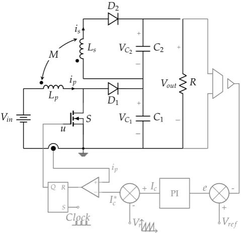
C2R
+
−
V
outC
1 +−
V
C1V
inu
S
M
Figure 1.Boost-flyback converter topology.
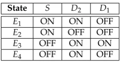
As the semiconductor devices are three, there are eight possible switch configurations or states: 88
E1... E8. However, it has been shown that only six states have physical meaning [23] and in [24] it
89
was proven that the controlled system exhibits a period-1 orbit switching among four states such as is 90
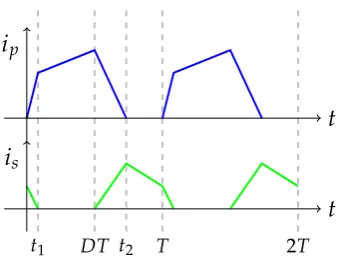
described in Table1. A schematic diagram of the steady state current behavior in a period-1 solution is 91
presented in figure2. The statesE1andE2are present when the MOSFET is on, and the statesE3and
92
E4are present when the MOSFET is off.
93
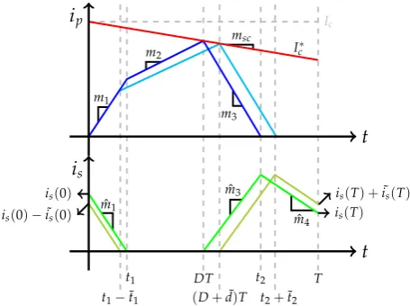
Table 1.States of the period-1 orbit
State S D2 D1
E1 ON ON OFF
E2 ON OFF OFF
E3 OFF ON ON
E4 OFF ON OFF
Starting fromE1the system evolves as follows:E17→E27→E37→E4. The change fromE1toE2is
94
given whenis =0 att=t1; the system changes fromE2toE3when the switching condition is satisfied
95
att=DT, which is called the duty cycle and corresponds to the ratio between the time the MOSFET is 96
on and the periodT,i.e:D=tu=1/T;E3changes toE4whenip=0 att=t2and finally att=Tthe
97
system returns toE1. The set of differential equations describing the period-1 orbit are:
t1 DT t2 T 2T
i
si
pt
t
Figure 2.Typical behavior of the currents flowing by the coils in steady state of a period-1 orbit.
• State 1:E1,t∈[kT kT+t1]:
99
dip
dt =
(LsVin+MVC2) n dis
dt =
(−MVin−LpVC2) n
dVC1
dt = −
(VC1+VC2) RC1
dVC2
dt =
is
C2
−(VC1+VC2)
RC2 (1)
• State 2:E2,t∈(kT+t1 kT+DT]:
100
dip
dt = Vin
Lp
dis
dt = 0
dVC1
dt = −
(VC1+VC2) RC1
dVC2
dt = −
(VC1+VC2) RC2
(2)
• State 3:E3,t∈(kT+DT kT+t2]:
101
dip
dt =
(Ls(Vin−VC1) +MVC2) n
dis
dt =
(−M(Vin−VC1)−LpVC2) n
dVC1
dt =
ip
C1
−(VC1+VC2) RC1
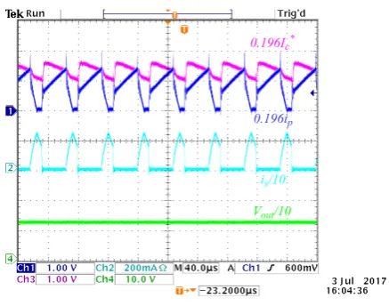
dVC2
dt =
is
C2
−(VC1+VC2) RC2
• State 4:E4,t∈(kT+t2 kT+T):
102
dip
dt = 0
dis
dt = −
VC2 Ls
dVC1
dt = −
(VC1+VC2) RC1
dVC2
dt =
is
C2
−(VC1+VC2) RC2
(4)
WhereVinis the input voltage,ipandisare the primary and secondary currents,VC1 andVC2 are 103
the voltages across the capacitorsC1andC2,M=kpLpLsis the mutual inductance which depends
104
on the coupling coefficientkandn=LpLs−M2. The output voltage isVout=VC1+VC2. 105
The peak current-mode control is a widely used technique for the control of power converters 106
[24,27,31]. A general schematic diagram of the boost-flyback converter with the proposed controller is 107
depicted in figure3. When a peak current-mode control is used, a fixed switching frequency is obtained 108
and the behavior of the currents are very similar to those depicted in figure2. At the beginning of the 109
period the MOSFET is active, the currentipgrows and the currentisdecreases down tois=0; at this
110
time instant (t1) the dynamical equations describing the system change but the MOSFET continues on
111
untilipis equal to the reference currentIc∗just att=DT. Att=DTthe switches turns off until the
112
next cycle starts again. The signalIc∗is composed by two parts: the first one (noted asIc) is provided
113
by a PI controller applied to the output voltage errore=Vre f −Vout. The second one corresponds to
114
the signal supplied by the compensation rampVr = ATrmod(t/T). In this way, the reference current
115
can be expressed as: 116
Lp ip
D1
Ls is
D2
C2 +
−
VC2
R
+
−
Vout
C1 +
−
VC1
Vin
u S M
-+
Vre f e
PI +
-Vr Ic Ic∗
−
+
ip
Q R
S Clock
Figure 3.Boost-flyback converter with peak current-mode control.
Ic∗ = kpe+ki Z
e dt− Ar
T mod(t/T) (5)
wherekpandkiare the parameters associated to the PI controller andArcorresponds to the amplitude
117
of the compensation ramp. Thanks to the flip-flop, there is only one switching cycle per period. At the 118
beginning of the period the switch turns on and it remains on until the switching conditionip=Icis
119
achieved (just the corresponding duty cycle). Whenip= Icthe switch opens and it holds opens until
120
the next period starts. Taking into account sliding is not possible (i.e.there is only one commutation 121
per cycle), the switching condition can be expressed as: 122
U= (
1 if 0≤t<DT,
0 ifDT≤t<T. (7)
WhereD∈[0, 1]is the duty cycle. 123
3. Slope Compensation Design 124
As far as the authors know, it has not been reported in the specialized literature a procedure to 125
determine the slope of the compensation ramp for a boost-flyback converter, such that can be used to 126
attain stability of the period-1 orbit. The objective of this section is to analyze the slopes of the currents 127
flowing through the inductors in order to find an analytical expression to determine the slope of the 128
compensation ramp, such that guarantees the stability of the period-1 orbit. In figure4, represents the 129
behavior of the currents flowing through primary and secondary coils when the system works in the 130
period-1 orbit described by statesE1,E2,E3andE4, and the slopes are clearly marked in the figure.
131
Ic
Ic∗
t1 DT t2 T
t1−˜t1 (D+d˜)T t2+t˜2
ˆ
m1
ˆ
m3
ˆ
m4 m1
m2
m3
msc
is(0)
is(0)−i˜s(0) is(T)
is(T) +i˜s(T)
t
t
is
i
pFigure 4.Primary- and secondary-coil currents for the period-1 orbit and a perturbed solution.
3.1. Assumptions 132
In the analysis, the following approximations are considered:i)for all elements and devices the 133
internal resistances are zero.ii)the steady state output of the PI-controller (Ic) is constant and hence
134
its derivative is zero; however, as it can be seen in the procedure, the constant value is not needed to 135
function of the duty cycleD.VC1 is just the output of the boost part,VC2 is the output of the flyback 137
part, taking into account the coupling factor is lower thank.1. 138
VC1 = 1
(1−D)Vin
VC2 =
(1− M Lp) (ML
s −1)
D
(1−D)Vin (8)
Vout =
1+(1−
M Lp) (LsM−1)D 1−D Vin.
andiv)all currents can be expressed mathematically like straight lines, such that the slopes associated 139
toiparem1,m2andm3, and the slopes associated tois are ˆm1, ˆm3and ˆm4(see figure4). These slopes
140
can be computed from equations (1), (2), (3) and (4), as follows: 141
m1 =
LsVin+MVC2 n ˆ
m1 =
−MVin−LpVC2 n m2 =
Vin
Lp (9)
m3 =
Ls(Vin−VC1) +MVC2 n
ˆ m3 =
−M(Vin−VC1)−LpVC2 n
ˆ
m4 = −
VC2 Ls
In a similar way as the slope compensation in a boost power converter is designed considering 142
the stability of the period-1 orbit [26], in this paper we propose an analysis of the stability of the 143
period-1 orbit using the information of the current slopes and the conditions that should be fulfilled to 144
guarantee the stability of the controlled system. To analyze the stability of the period-1 orbit a small 145
perturbation is added at the beginning of the cycle and its corresponding value at the end of the period 146
Tis computed. If the magnitude of the perturbation increases, then the period-1 orbit is unstable; on 147
the contrary, if the magnitude of the perturbation decreases, then the orbit is stable. 148
149
3.2. Mathematical Procedure 150
Analysis of current in the primary coil 151
At the swiching timet=DTa pair of equations are fulfilled: One of them to its left and the other one to its rigth. Defining the slope of the compensation ramp asmsc = ArT , it can be seen that just at the switching time the following equation is satisfied:
Ic−mscDT =m1t1+m2(DT−t1) (10)
Considering a perturbation in the initial condition, the last equation can be expressed as:
Subtracting equation (11) from (10), we obtain:
mscdT˜ =m1t˜1−m2(dT˜ +t˜1) (12)
From (12)
˜ t1=
(msc+m2) (m1−m2)
˜
dT (13)
In a similar way, the analysis at the right of the switching time leads to the next equation.
Ic−mscDT−m3(t2−DT) =0 (14)
Taking into account the perturbation, this equation is given by:
Ic−msc(D+d˜)T−m3((t2+t˜2)−(D+d˜)T) =0 (15)
Subtracting (15) from (14)
mscdT˜ +m3(t˜2−dT˜ ) =0 (16)
From (16),
˜ t2=
(m3−msc)
m3
˜
dT (17)
152
Analysis of current in the secondary coil 153
Now, the expressions for the currentisand its perturbation ˜is(0)are computed. Att=t1they are:
is(0)−mˆ1t1=0 (18)
and
is(0)−i˜s(0)−mˆ1(t1−t˜1) =0 (19)
Subtracting (19) from (18), it is obtained
˜
is(0) =mˆ1t˜1 (20)
Replacing (13) in (20), we have: ˜
is(0) =mˆ1
(msc+m2) (m1−m2)
˜
dT (21)
From this equation ˜dTcan be expressed as:
˜
dT= i˜s(0)
ˆ
m1((mmsc1−+mm22))
(22)
Now, att=t2the following equation is fulfilled,
ˆ
m3(t2−DT)−mˆ4(T−t2) =is(T) (23) At the same timet=t2, the perturbed equation is:
ˆ
Now, subtracting (23) from (24), we have:
˜
is(T) = (mˆ3+mˆ4)t˜2−mˆ3dT˜ (25)
Replacing (17) en (25), we obtain:
˜ is(T) =
ˆ m4−msc
(mˆ3+mˆ4)
m3
˜
dT (26)
Finally, replacing equation (22) in (26) we find an expression that relates the secondary coil current at the beginning of the cycle, with its value at the end of it. This expression is given by:
˜
is(T) =αi˜s(0) (27)
where
α=
(mˆ4−msc(mˆ3m+3mˆ4)) ˆ
m1((mmsc+m2)
1−m2)
(28)
Stability condition 154
Then, the stability of the period-1 orbit is given by the absolute value ofα. If|α|>1 the periodic
orbit is unstable, if|α| < 1 it is asymptotically stable, and|α| = 1 corresponds to the limit of the
stability. To guarantee that the system operates in a period-1 orbit the slope of the compensation ramp must satisfy the following expression:
msc= Ar
T >
m3(mˆ4(m1−m2)−mˆ1m2)
ˆ
m1m3+ (mˆ3+mˆ4)(m1−m2) (29)
4. Results 155
4.1. Numerical Results 156
The parameter values used for simulations and experiments are given in Table2. The voltages 157
VC1 andVC2 are computed from equation (8), the slopes of the straight lines are calculated using 158
equation (9), the output voltageVoutcorresponds to the desired output voltageVre f and|α|=1. With
159
these data, the desired output voltage is varied and the limit value of the slope compensationmscis
160
obtained. Figure5(a) shows the results obtained when the proposed approach is used (see (29)) and 161
Vre f ∈(90, 130). Figure5(b) presents the exact computation using the saltation matrix. Values ofAr
162
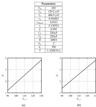
grater than the stability limit guarantee stability of a period-1 orbit. In addition, forVre f =100Vthe
163
limit value for the compensation ramp is close toAr =1.94 and forVre f =120Vis close toAr=3.25
164
(see figure5). Figure6shows the comparison between the analytical approach proposed in this paper 165
and the exact value obtained with the saltation matrix; the result is expressed in percentage of the error. 166
As it is shown, the lower the reference voltage, the higher error there is. In fact, for gain factors upper 167
than six, the approach behaves better. 168
4.2. Experimental results 169
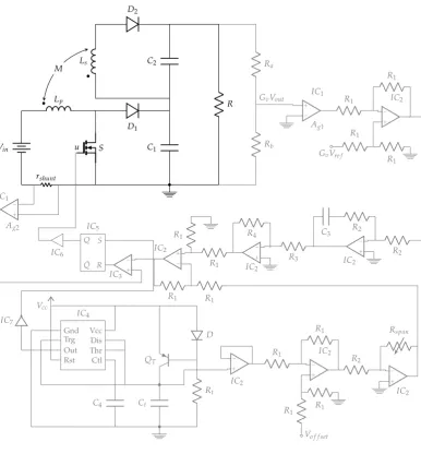
To validate the numerical results, an experimental lab prototype able to deliver 100 Watts to the 170
load was designed and implemented as it is shown in figure7. A complete design of the circuit is 171
shown in rigure8. A ferrite core typeEis used to design the coupled inductors and the number of 172
turns were calculated with the approach proposed in [36]. The values of the different elements of the 173
circuit are given in Tables2and3. The current in the primary coil is measured with a non-inductive 174
shunt-resistancershunt(LTO050FR0100FTE3) followed by an instrumentation amplifierIC1; the output
175
voltage is measured through a voltage divider which consists ofRaandRb. The signal from the voltage
Table 2.Parameter values of the converter
Parameters
Vin 18V
Lp 129.2µH
Ls 484.9µH
rp 0.0268Ω
rshunt 0.01Ω
rs 0.1307Ω
k 0.995
C1 220µF
C2 220µF
R 200Ω
kp 2
ki 350
T 1/(20KHz)
90 100 110 120 130
1 2 3 4
90 100 110 120 130
1 2 3 4
(a) (b)
Figure 5. Value of the slope compensation. (a) Approach proposed in this paper. (b) Exact value obtained with the saltation matrix.
90 100 110 120 130 0
20 40 60 80 100
Figure 6.Percentage of error of the slope compensation.
divider feeds other amplifierIC1. TheMOSFETis anIRFP260Nwhich has low internal resistance.
177
Finally, two ultra-fast diodesRHRP30120 (D1andD2) are used.
178
The controller is implemented using operational amplifiers (IC2). The compensation ramp and
179
the clock signals are generated using anLM555 (IC4). The amplitude of the compensation ramp
180
is adjusted with a span resistorRspan andVB compensates the offset. The constantskpandki are
181
associated to the PI controller, and they are obtained fromR2,R3,R4andC3. The measured signals
Figure 7.Experimental implementation
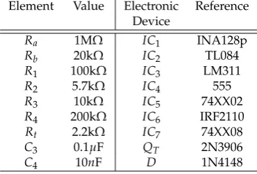
Table 3.Other parameter associated to the experiment.
Element Value Electronic Reference Device
Ra 1MΩ IC1 INA128p
Rb 20kΩ IC2 TL084
R1 100kΩ IC3 LM311
R2 5.7kΩ IC4 555
R3 10kΩ IC5 74XX02
R4 200kΩ IC6 IRF2110
Rt 2.2kΩ IC7 74XX08
C3 0.1µF QT 2N3906
C4 10nF D 1N4148
were scaled to 0.196 using the voltage gains (Ag1 andAg2). The constantGvis given by the voltage 183
dividerRb/(Ra+Rb).
184
Four experiments to validate the results obtained in the previous section are carried out. All 185
figures of the experimental results show the reference currentIc∗, the current in the primary coilip,
186
the current in the secondary coilisand the output voltageVout. Therefore, the output voltage and the
187
current in the secondary coil are scaled by a factor of 10. The reference current and the current in the 188
primary coil are scaled by a factor of 0.196 as it was mentioned before. 189
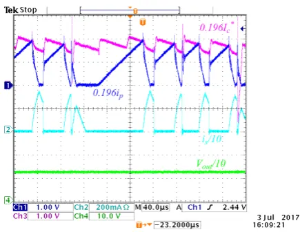
ForVre f = 100V (the load resistance is fixed toR = 200Ω, Table 2), two values of the slope
190
compensation are tuned:Ar =1.8 andAr =2.2. WhenAr =1.8 the limit set is a period-2 orbit as it
191
shows in figure9, but if the ramp compensation increases toAr =2.2, it changes to a period-1 orbit
192
Vin
Lp
D1
C1 S
rshunt
C2 Ls
D2
R M
u
Ra
Rb
GvVout
−
+
IC1
Ag1
R1 −
+
IC2
R1
R1
R1
GvVre f
R2 −
+
IC2
R2
C3
R3 −
+
IC2
R4
R1
−
+ IC2
R1
R1
R1 −
+
IC3 −
+
IC1
Ag2 IC5
Q
¯ Q
S
R IC6
Vcc Dis Thr Ctl Gnd Trg Out Rst
IC4
Vcc
Ct
D
Rt
C4
QT −
+
IC2
R1 −
+
IC2
R1
R1
R1
Vo f f set
R2 −
+
IC2
Rspan
IC7
Figure 8.Experimental Circuit.
Figure 10.ipforVre f =100V andAr=2.2.
In the second experimentVre f =120V. In a similar way, two values of the slope compensation
194
are tuned:Ar =3 andAr=3.4. The behavior ofIc∗,ip,isandVoutare shown in figures11and12. For
195
Ar =3 a high-period orbit appears, and forAr =3.4 the period-1 orbit is stable. These results agree
196
with the information provided by equation (29), and this formula is adequate for tuning the slope of 197
the compensation ramp. 198
5. Conclusions 199
This paper enhances the knowledge of the controller design for a boost-flyback converter which 200
is currently a field of study. 201
To obtain high gains with a stable period-1 orbit when a boost-flyback converter is used, it is 202
necessary to add a compensation ramp in the design. In this paper, an analytical expression to compute 203
the value of the compensation ramp slope was found and mathematically proven. For gains greater 204
than six, the approach developed in this paper has an error lower than 5%. 205
In a general way, the results obtained from the equation derived from our computations agree 206
with the experiments, there is a small disagreement in comparison with the exact solution for gains 207
lower than six, mainly because some of the assumptions are to strong for the real system, which were 208
not included in the model for the sake of simplicity. This difference is neglectable for high step-up 209
gains, for which our approach provides the major benefit of having a formula to guarantee stability 210
avoiding over-compensation or very complex computations. 211
Figure 12.ipforVre f =120V andAr=3.4
Author Contributions:Conceptualization, Fabiola Angulo; Formal analysis, Juan-Guillermo Muñoz and Fabiola 212
Angulo; Funding acquisition, Fabiola Angulo and Gustavo Osorio; Investigation, Juan-Guillermo Muñoz; 213
Project administration, Fabiola Angulo; Software, Juan-Guillermo Muñoz, Guillermo Gallo and Gustavo Osorio; 214
Supervision, Fabiola Angulo and Gustavo Osorio; Validation, Juan-Guillermo Muñoz; Writing – original draft, 215
Juan-Guillermo Muñoz and Guillermo Gallo; Writing – review editing, Fabiola Angulo and Gustavo Osorio. 216
FundingThis work was supported by Universidad Nacional de Colombia, Manizales, Project 31492 from 217
Vicerrectoría de Investigación, DIMA, and COLCIENCIAS under Contract FP44842-052-2016 and program 218
Doctorados Nacionales 6172-2013. 219
Acknowledgments:The authors would like to thank Dr. Ángel Cid Pastor and Dr. Abdelali el Aroudi from GAEI 220
Research Center, Universitat Rovira i Virgili, SPAIN, for their assistance in getting experimental results. 221
Conflicts of Interest:The authors declare no conflict of interest. The founding sponsors had no role in the design 222
of the study; in the collection, analyses, or interpretation of data; in the writing of the manuscript, and in the 223
decision to publish the results. 224
Appendix A 225
In this appendix, the procedure to find the ratio between input and output voltages for a flyback converter when copuling factorkis different from zero is presented
VC2 =
n2
n1
D
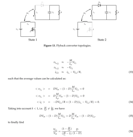
1−D (30)
The flyback converter operates in two topologies named state 1 and state 2, which are depicted in figure13. 226
Voltage equations in primary and secodary coils are given in general form as: 227
vLp = Lp
dip
dt +M dis
dt
vLs = Ls
dis
dt +M dip
dt. (31)
Depending on the state, voltages and currents can be approximated as: 228
State 1 229
vLp1 ≈ Vin
vLs1 ≈
M LpVin
iC1 ≈ −VC2/R (32)
Lp
Ls D2
C2 R
Vin
uS ML
Lp
Ls
D2
C2 R
Vin
u
S ML
State 1 State 2
Figure 13.Flyback converter topologies.
vLp2 ≈ −
M Ls
VC2
vLs2 ≈ −VC2
iC2 ≈ iLs−VC2/R, (33)
such that the average values can be calculated as: 231
<vLp > = DVin−(1−D)
M LsVC2
=0
<vLs > = D
M Lp
Vin−(1−D)VC2=0
<iC> = −DVC2/R+ (1−D)(iLs−VC2/R) =0. (34)
Taking into accountk<1, i.e. LpM 6= LsM, we have 232
DVin−(1−D)
M LsVC2
=DM
LpVin
−(1−D)VC2, (35)
to finally find 233
VC2
Vin
=
(1− M
Lp)
(MLs−1) D
(1−D) (36)
Doingk=1, it is easy to prove that this ratio is the same as the reported for a non magnetically coupled 234
flyback converter. 235
236
1. Wu, Y.E.; Chiu, P.N. A High-Efficiency Isolated-Type Three-Port Bidirectional DC/DC Converter for 237
Photovoltaic Systems. Energies2017,10. 238
2. Choudhury, T.R.; Dhara, S.; Nayak, B.; Santra, S.B. Modelling of a high step up DC-DC converter based on 239
Boost-flyback-switched capacitor. 2017 IEEE Calcutta Conference (CALCON), 2017, pp. 248–252. 240
3. Shen, C.L.; Chiu, P.C. Buck-boost-flyback integrated converter with single switch to achieve high voltage 241
gain for PV or fuel-cell applications. IET Power Electronics2016,9, 1228–1237. 242
4. Lodh, T.; Majumder, T. Highly efficient and compact Sepic-Boost-Flyback integrated converter with 243
multiple outputs. 2016 International Conference on Signal Processing, Communication, Power and 244
Embedded System (SCOPES), 2016, pp. 6–11. 245
5. Arango, E.; Ramos-Paja, C.A.; Calvente, J.; Giral, R.; Serna, S. Asymmetrical Interleaved DC/DC Switching 246
Converters for Photovoltaic and Fuel Cell Applications-Part 1: Circuit Generation, Analysis and Design. 247
6. Liu, H.; Hu, H.; Wu, H.; Xing, Y.; Batarseh, I. Overview of High-Step-Up Coupled-Inductor Boost 249
Converters. IEEE Journal of Emerging and Selected Topics in Power Electronics2016,4, 689–704. 250
7. Wang, Y.F.; Yang, L.; Wang, C.S.; Li, W.; Qie, W.; Tu, S.J. High Step-Up 3-Phase Rectifier with Fly-Back Cells 251
and Switched Capacitors for Small-Scaled Wind Generation Systems.Energies2015,8, 2742–2768. 252
8. Zhao, Q.; Lee, F.C. High performance coupled-inductor DC-DC converters. Applied Power Electronics 253
Conference and Exposition, 2003. APEC ’03. Eighteenth Annual IEEE, 2003, Vol. 1, pp. 109–113 vol.1. 254
9. Tseng, K.; Liang, T. Novel high-efficiency step-up converter.Electric Power Applications, IEE Proceedings
-255
2004,151, 182–190. 256
10. Liang, T.; Tseng, K. Analysis of integrated boost-flyback step-up converter. Electric Power Applications, IEE
257
Proceedings -2005,152, 217–225. 258
11. Xu, D.; Cai, Y.; Chen, Z.; Zhong, S. A novel two winding coupled-inductor step-up voltage gain 259
boost-flyback converter. 2014 International Power Electronics and Application Conference and Exposition
260
2014, pp. 1–5. 261
12. Zhang, J.; Wu, H.; Xing, Y.; Sun, K.; Ma, X. A variable frequency soft switching boost-flyback converter for 262
high step-up applications. 2011 IEEE Energy Conversion Congress and Exposition, 2011, pp. 3968–3973. 263
13. Ding, X.; Yu, D.; Song, Y.; Xue, B. Integrated switched coupled-inductor boost-flyback converter. 2017 264
IEEE Energy Conversion Congress and Exposition (ECCE), 2017, pp. 211–216. 265
14. Lai, C.M.; Yang, M.J. A High-Gain Three-Port Power Converter with Fuel Cell, Battery Sources and Stacked 266
Output for Hybrid Electric Vehicles and DC-Microgrids. Energies2016,9. 267
15. Tseng, K.C.; Lin, J.T.; Cheng, C.A. An Integrated Derived Boost-Flyback Converter for fuel cell hybrid 268
electric vehicles. 2013 1st International Future Energy Electronics Conference (IFEEC), 2013, pp. 283–287. 269
16. Park, J.H.; Kim, K.T. Multi-output differential power processing system using boost-flyback converter 270
for voltage balancing. 2017 International Conference on Recent Advances in Signal Processing, 271
Telecommunications Computing (SigTelCom), 2017, pp. 139–142. 272
17. Chen, S.M.; Wang, C.Y.; Liang, T.J. A novel sinusoidal boost-flyback CCM/DCM DC-DC converter. 2014 273
IEEE Applied Power Electronics Conference and Exposition - APEC 2014, 2014, pp. 3512–3516. 274
18. Lee, S.W.; Do, H.L. A Single-Switch AC-DC LED Driver Based on a Boost-Flyback PFC Converter With 275
Lossless Snubber. IEEE Transactions on Power Electronics2017,32, 1375–1384. 276
19. Divya, K.M.; Parackal, R. High power factor integrated buck-boost flyback converter driving multiple 277
outputs. 2015 Online International Conference on Green Engineering and Technologies (IC-GET), 2015, pp. 278
1–5. 279
20. V. Acary, O.B.; Brogliato, B.Nonsmooth Modeling and Simulation for Switched Circuits; Springer, 2011. 280
21. Banerjee, S.; Verghese, G. Nonlinear Phenomena in Power Electronics: Bifurcations, Chaos, Control, and
281
Applications; Wiley-IEEE Press, 2001. 282
22. Di Bernardo, M.; Budd, C.; Champneys, A.; Kowalczyk, P.Piecewise-smooth Dynamical Systems, Theory and
283
Applications; Springer, 2008. 284
23. Carrero Candelas, N.A. Modelado, simulación y control de un convertidor boost acoplado magnéticamente. 285
PhD thesis, Universidad Politécnica de Catalunya, 2014. 286
24. Munoz, J.G.; Gallo, G.; Osorio, G.; Angulo, F. Performance Analysis of a Peak-Current Mode Control with 287
Compensation Ramp for a Boost-Flyback Power Converter.Journal of Control Science and Engineering2016. 288
25. Muñoz, J.G.; Gallo, G.; Angulo, F.; Osorio, G. Coexistence of solutions in a boost-flyback converter with 289
current mode control. 2017 IEEE 8th Latin American Symposium on Circuits Systems (LASCAS), 2017, pp. 290
1–4. 291
26. Erickson, R.W.; Maksimovic, D.Fundamentals of Power Electronics; Springer, 2001. 292
27. Jiuming, Z.; Shulin, L. Design of slope compensation circuit in peak-current controlled mode converters. 293
Electric Information and Control Engineering (ICEICE), 2011 International Conference on, 2011, pp. 294
1310–1313. 295
28. Grote, T.; Schafmeister, F.; Figge, H.; Frohleke, N.; Ide, P.; Bocker, J. Adaptive digital slope compensation 296
for peak current mode control. Energy Conversion Congress and Exposition, 2009. ECCE 2009. IEEE, 2009, 297
pp. 3523–3529. 298
29. Chen, Y.; Tse, C.K.; Wong, S.C.; Qiu, S.S. Interaction of fast-scale and slow-scale bifurcations in current-mode 299
30. Chen, Y.; Tse, C.K.; Qiu, S.S.; Lindenmuller, L.; Schwarz, W. Coexisting Fast-Scale and Slow-Scale Instability 301
in Current-Mode Controlled DC/DC Converters: Analysis, Simulation and Experimental Results. IEEE
302
Transactions on Circuits and Systems I: Regular Papers2008,55, 3335–3348. 303
31. Fang, C.C.; Redl, R. Subharmonic Instability Limits for the Peak-Current-Controlled Buck Converter With 304
Closed Voltage Feedback Loop. IEEE Transactions on Power Electronics2015,30, 1085–1092. 305
32. Fang, C.C.; Redl, R. Subharmonic Instability Limits for the Peak-Current-Controlled Boost, Buck-Boost, 306
Flyback, and SEPIC Converters With Closed Voltage Feedback Loop. IEEE Transactions on Power Electronics
307
2017,32, 4048–4055. 308
33. El Aroudi, A. A New Approach for Accurate Prediction of Subharmonic Oscillation in Switching Regulators 309
Part I: Mathematical Derivations. IEEE Transactions on Power Electronics2017,32, 5651–5665. 310
34. El Aroudi, A. A New Approach for Accurate Prediction of Subharmonic Oscillation in Switching Regulators 311
Part II: Case Studies.IEEE Transactions on Power Electronics2017,32, 5835–5849. 312
35. Leine, R.I.; Nijmeijer, H.Dynamics and Bifurcations of Non-Smooth Mechanical Systems; Springer, 2004. 313