666
An Architecture To Detect And Debug The Latency Using Pulse
Generator
G.S.Sankari
Assistant Professor/ECE,M.A.M College of Engineering And Technology,Trichy.
Abstract-The on-chip path delay measurement techniques have been gained many attentions, since it provides a cost effective alternative way to perform delay defect detection and silicon debug in modern VLSI chips. Rather than testing the chips with all possible worst case test vectors and process corners,it is better to measure the delays of paths and to check if the slacks are large enough to tolerate all the possible delay variations.Therfore the worst case test vectors considering different sources of variations can be avoided and high test confidence can be obtained.Herea on-chip path delay measurement architecture is used for detecting and debugging delay faults in the integrated circuits.Number of delay stages are employed in on-chip delay measurement architecture circuit, whose delay ranges are increased by a factor of two gradually from the last to the first stage. And also a calibration circuit is incorporated into the circuit to calibrate the delay range of the delay stage. The area overhead is also reduced in this technique.
I.INTRODUCTION
Scaling of transistors is an essential case of vlsimanufacturing,as scaling increases the capacity of the integrated circuits increases.Hence it is difficult to perform the functional operation with the number of gates and transistors. Also the delay caused due to the increased complexity may degrade the performance of the circuits.There are certain timing defects formed from the manufacturing process are resistive opens,metalmouseetc.,Also certain electrical parameters causes the delay defects such as threshold voltage,parasitic capacitance ,channel length and current saturation.The temperature related defects such as environmental variations also leads to increased delays.
Such delay defects may leads to failure of the entire system,and the efficiency decreases. Hence testing is very essential in those cases and calculating the delays and debug if any fault is in the system.
A new on-chip path delay measurement structure called path based ring oscillator is used. It creates an oscillator from a targeted path for which it is used to measure path delay on-chip under the impact of process variation.To alleviate accuracy degrationcaused by the architecture itself,a high
accuracy calibration process is required.Ring oscillator can be used more efficiently for path delay measurement by making the path under test part of the oscillator.With the help of the oscillator,delay on path and its returning loop can be translated into oscillation frequency which can be easily read out by the counter with no potential accuracy loss.
It utilizes existing paths to form path-RO instead of inserting extra ring oscillators,which ensures better understanding of process variations impact on path delay. As a result, intra/inter die process variations impact on path delay can be obtained by comparing simulated and measured path delay results.With continues scaling of technology and decreasing clock cycle, delay introduced by returning loop connecting the output and input of PUT will greatly impact the measured oscillation frequency. To improve the accuracy of path delay measurement ,the extra delay introduced by returning loop is obtained using a calibration process and could be easily removed from measured data.But the timing resolution is a limitation over this technique.
II.RELATED WORKS
A built in parametric measurement circuit for time interval measurement based on the dual slope technique is introduced. The capacitor is first charged by the input voltage with a high slope and then the capacitor is discharged with a known lower slope. Therefore the time interval can be derived from the discharging time based on the propositional tome between the discharge time and the input voltage.
667
A built in delay sensing circuit to improve the delay fault coverage of the CUT. The delay of the path under test is converted to a certain voltage height by using a sawtooth waveform generated from reference clock signal. By comparing the converted voltage with the reference voltage. Delay fault of the target path can be detected.
An ATE- based test architecture and test per scan BIST architecture using delay sensing hardware is used in delay testing. A probe point inversion algorithm for transition delay faults begins by creating graph. There are two main objectives to be considered while choosing the probing points. To reduce the number of test vectors and thus the test time and to increase the fault coverage. Hence a delay fault testing methodology using an on-die delay sensor, Low overhead. Here offset voltage and the settling time are the limitations .
An On-chip scheme for delay fault detection and performance characterization is proposed in this paper. In this method, A modified Vernier delay line which is used to characterize the critical path delay is used.
The modified Vernier Delay Line was designed in 0.18 micro meter CMOS technology. Wallace and Dadda multipliers of different sizes were use as test circuits. A commercial static timing analysis tool is used to extract the top critical path for each circuit as well as the delay of critical path. Each such critical path was then sensitized for worst case propagation delay and range of the delay values was measured using the MVDL. The input and the output of each critical path were connected to the x and y inputs of MVDL respectively.These circuits offers good resolution,robustness and takes less time for measurement,but the higher output range the area overhead is huge
.
III.PROPOSED WORK
A.OCDD CIRCUIT
This circuit is used for path delay testing measurement in order to measure a large delay measurement range.The objective of this method is to reduce the number of delay stages should reduced hence the area overhead also reduced.
The structure of OCDD can convert the path delay of the circuit under test into series of digital values which are stored in its respective buffers in the circuit.Each delay stages consist of a positive triggered D-flipflop. The d-flip-flop can capture the value of the D-input at a definite portion of the clockcycle such as
the rising edge of the clock.The advantage of using D-flip-flop is that the signal on the D-input pin is captured the moment the flip-flop is clocked an subsequent changes on the D-input will be ignored until the next clock event.
The input and output of the path under measurement is given to the corresponding y and x of the on chip delay detection circuit. A delay stage consists of a upper delay chain and a lower delay chain.The upper chain is starts from the input y of the circuit and ends at the input of the multiplexer whose output is connected to the data input of the flip-flop in each delay stage.Similarly, the lower delay chain it starts from the output x of the circuit.
The delay range is defined as the delay difference between the two delay units in each delay stage of the OCDD circuit.In the last stage of the UDU the delay is named as Dbuf_1 is larger than that of the last delay stage LDU,the delay for LDU is Dbuf_2. Rlast= Dbuf_1 - Dbuf_2.
The DC compensation circuit is used in the OCDD circuit.Here two rising transition from the path under measurement is passes through the DC unit and then go into the inputs of the first delay stage of the OCDD circuit respectively.
Fig.1 On chip delay measurement circuit
668
If the time difference of the two inputs in the flip-flop is lesser than that of the set up time an logic error will be hold in the buffer. So in-order to solve this problem a DC circuit is implemented,which consists of two buffers. This is made in-order to compensate the upper and lower delay units with the set up time. The values which are stored in the delay chain will be shifted out serially with the help of the shiftclk, kept in shiftmode and de-asserting the mode signal. Thus the delay of the path under measurement can be obtained.
B. CALIBRATION CIRCUIT:
In order to assure the precision of path delay measurement result before using the OCDD circuit.Because the delay range of each delay stage in the OCDD circuit would be varied due to prominent process variation.
Fig.2 Calibration circuit
In the calibration circuit,when CS=1,transitions at Pin,Pout can be sent into OCDD circuit for delay measurement.When CS=0, the delay range calibration process is conducted.Initially, the flip flops are in logic 0 by asserting he reset signal.Then logic 1 will be applied to flipflop1 and 2 by rising and falling edges of clock signal.The time difference between the generated rising transitions at y and x is equal to the width of positive half cycle of clock signal.
C. SIGNAL TO TRANSITION CONVERTER:
As mentioned in the previous section, the OCDM circuit works well only when the input and output of the PUM are rising transitions. However, there are other three additional cases possibly to activate the worst case delay of a circuit path, such as a path in which the input is a rising transition and the
output is a falling transition. It is thus better to transfer the output signal into the signal with rising transition for facilitating path delay measurement regardless of the transition direction of the original signal. The STC block is used to handle this problem. Therefore, rising transitions which are derived from the start and end points of PUM can be fed into the inputs and of the OCDD circuit, the basic structure of the STC block, which is previously designed for signal stability violation detection .The simplified timing waveform for the STC block. When the pre-charge signal is low, denoted as the pre-charge period, both the nodes and are charged up to logic high values. Hence the OUT signal keeps a logic low value. Clearly, if a rising transition is generated at the IN signal when the pre-charge signal is high, both the nodes and are discharged to logic low values after the arrival of the rising transition of IN. Therefore, a rising transition is generated at the OUT signal. Likewise, a rising transition would also be generated at the OUT signal after the arrival of a falling transition of the IN signal. Hence, by using the STC block, the input signal with arbitrary transition direction can be converted into a rising transition signal for facilitating path delay measurement.
Fig.3 Signal To Transition Converter
669
D. PULSE GENERATOR
Pulse generator is used to control the frequency,pulse width, delay with respect to an internal or external trigger and high and low voltage level of the pulses. It will allow control over the rise time and fall time of the pulses. Pulse generators are voltage sources, they are available for generating pulses having widths ranging from minutes down to under 1 picoseconds. Pulse generator uses digital ,analog, or combinational of both technique to form the output pulses..
Pulses can then be injected into the DUT and used as a stimulus or clock signal are analysed as they progress the high pulse through the device,confirming the proper operation of the device or pinpointing a fault in the device. Pulse generator are also used in devices such as switches,lasers and optical components,modulators and resistive loads. The output of pulse generator may be used as the modulation signal for a signal generator.
E.PATH DELAY MEASUREMENT ARCHITECTURE
By using the proposed technique, the selected critical paths will be able to find an effective way to calculate the optimal path for direct measurement or by the calculation of measured delays. Initially the paths for delay measurement has to be selected,for each PUM the input and its corresponding output transitions of paths are given to the OCDD circuit for measuring delay. The first vector pair of the PUM is given to the circuit in order to initialize the logic to a stable state. Then by asserting the reset signal all the flip- flops are initialised to logic zero and also by asserting the mode signal delay measurement mode is activated .again the second vector of the test vector pair is applied to the circuit,atransision will be activated and propagated from the input to the output signal hence the delay difference of the two transition signal can be measurement can be measured by the OCDD circuit.After the completion of the delay measurement, the circuit is shifted to the next flip-flop by de-assserting the mode signal.Hence the values stored are serially shifted to the parallel delay line using shiftclock. The values can be calculated from the consequent measures from readout. By doing so, all the paths can be measured for delay.
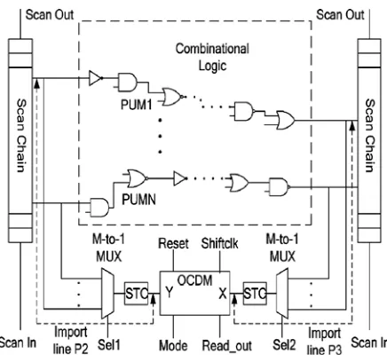
F. PATH UNDER MEASUREMENT
The path selected for delay measurement can be timing-critical paths whose delays exceed the specified timing threshold under static timing analysis.The architecture of the proposed path delay measurement scheme using the OCDDcircuit . The paths selected for delay measurement can be timing-critical paths whose delays exceed the specified timing threshold under static timing analysis (STA) or statistical STA . Based on the selected timing-critical paths, the method proposed provides an effective way to further find an optimal path set for measurement, while the delays of all the selected timing-critical paths can be obtained either by direct measurement or by calculation from the measured delays. In this paper, we mainly focus on the design of the path delay measurement architecture. Two M-to-1 multiplexers are included aiming to select a particular path into the OCDM circuit for delay measurement.
.
Fig .4 Path Delay Measurement Architecture
670
Fig 5.Output Of Calibration Circuit
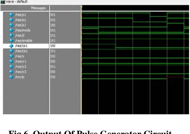
Fig.6. Output Of Pulse Generator Circuit
Fig 7.Output Of Path Under Measurement Architecture
connected to the calibration circuit, to precisely measure the delay range of each delay stage. Because the delay range may be vary due to process variation.
The delay difference of the import lines for feeding the start and end transitions of PUM into the OCDD circuit,which is used to provide a high precision for measurement of path delay. By using this method, the delay stages are reduced when comparing with the other conventional techniques. Hence the area overhead is also reduced.
IV.CONCLUSION
The system designed in this project is a on-chip path delay measurement architecture ,whose delay ranges are increased by a factor of two from the large to the first stage. The path under measurement is given to the pulse generator, which is used to have sharp transitions with normal impact due to process variability. In order to calculate the error introducedduring pulse generation,a specific mode is being implemented in the circuit. The delay compensation circuit also implemented into OCDD circuit. The time difference between the inputs of the store block is smaller than the setup time, an error logic may be hold in the flip-flop. To avoid this problem,and to provide better resolution DC circuit is proposed. The PUM is
V.REFERENCES
[1] A. Agarwal, D. T. Blaauw, and V. Zolotov, “Statistical timing analysis using bounds and selective enumeration,” IEEE Trans. Comput.-AidedDesignIntegr. Circuits Syst., vol. 22, no. 9, pp. 1243–1260, Sep. 2003.
[2] A. Agarwal, D. Blaauw, and V. Zolotov, “Statistical timing analysis for intra-die process variations with spatial correlations,” in
Proc.IEEE/ACM Int. Conf. Comput.-Aided Design,
2003, pp. 271–276.
[3] A. Krstic and K. T. Cheng, Delay Fault Testing for VLSI Circuits.Boston, MA: Kluwer, 1998.
[4] A. Kristic, J.-J. Liou, Y.-M.Jaing, and K. T. Cheng, “Delay testing considering crosstalk-induced effects” in Proc.IEEEInt.test Conf.,2001,pp.558-567.
[5] A. Raychowdhury, S. Ghosh, and K. Roy, “A novel on-chip delay measurment hardware for efficient speed-binning,” in Proc. IEEE Int.On-Line Test. Symp., 2005, pp. 287–292.
[6] B. Kruseman, A. K. Majhi, G. Gronthoud, and S. Eichenberger, “On hazard-free patterns for fine-delay fault testing,” in Proc. IEEE Int. TestConf., 2004, paper 9.1.
671
[8] F. Xiang, H. Li, and X. Li, “Robust test generation for power supply noise induced path delay faults,” in
Proc. IEEE Asia South Pacific DesignAutom. Conf.,
2008, pp. 659–662.
[9] G. Yan, Y. Han, and X. Li, “A unified online fault detection scheme via checking of stability violation,”
in Proc. IEEE/ACM Design, Autom.,Test Euro. Conf.
Exhib., 2009, pp. 496–501.
[10] H. Balachandran, K. Butler, and N. Simpsoon, “Facilitating rapid first silicon debug,” in Proc. IEEE Int. Test Conf., 2002, pp. 628–637.
[11] J. D. Lesser and J. J. Shedletsky, “An experimental delay test generator for LSI logic,” IEEE Trans. Comput.,vol. C-29,no.3,pp 235-248,Mar.1980.
[12] J. M. Rabaeyet al., Digital Intergrated Circuits: A
Design Perspective, 2nd ed. Englewood Cliffs, NJ:
Prentice-Hall, 2003.
[13] K. Baker, G. Gronthoud, M. Lousberg, I. Schanstra, and C. Hawkins, “Defect-based delay testing of resisitivevias-contacts: A critical evaluation,” in Proc. IEEE Int. Test Conf., 1999, pp. 467–476.
[14] M. Agarwal, B. C. Paul, M. Zhang, and S. Mitra, “Circuit failure prediction and its application to transistor aging,” in Proc. IEEE VLSI TestSymp., 2007, pp. 277–286.
[15] M. Favalli and C.Metra, “Sensing circuit for on-line detection of delay faults,” IEEE Trans. Very Large Scale Integr. (VLSI) Syst., vol. 4, no. 1, pp. 130–133, Jan. 1996.
[16] M. Hsiao, J. Huang, S. Yang, and T. Chang, “A built-in timing parametric measurement unit,” in Proc. IEEE Int. Test Conf., 2001, pp. 315–322.
[17] M. Tsai, C. Cheng, and C. Yang, “An all-digital high-precision built-in delay timemeasurement circuit,” in Proc. IEEE VLSI Test Symp., 2008, pp. 249–254.
[18] M. Yilmaz, K. Chakrabarty, and M. Tehranipoor, “Test-pattern grading and pattern selection for small-delay defects,” in Proc. IEEE VLSI TestSymp., 2008, pp. 233–239.
[19] M. Zhang, H. Li, and X. Li, “Multiple coupling effects oriented path delay test generation,” in Proc. IEEE VLSI Test Symp., 2008, pp. 383–388
[20] N. Ahmed, M. Tehranipoor, and V. Jayaram, “A novel framework for faster-than-at-speed delay test considering IR-drop effects,” in Proc.IEEE/ACM Int. Conf. Comput.-Aided Design, 2006, pp. 198–203.
[21] P. Nigh and A. Gattiker, “Test method evaluation experiments and data,” in Proc. IEEE Int. Test Conf., 2000, pp. 454–463
[22] R. Tayade and J. A. Abraham, “Small-delay defect detection in the presence of process variations,” Microelectron. J., vol. 39, no. 8, pp. 1093–1100, Aug. 2008.