A New Fuzzy based closed-loop Buck Boost Converter
for Power Factor Correction
GODISELA MONISHA GOUD
M-tech Student Scholar
Department of Electrical & Electronics Engineering, Malla Reddy Engineering College (Autononomous), Maisammaguda;
Hyderabad; Telangana, India.
Mr. J. MUNI CHANDRA SHEKAR
Assistant Professor
Department of Electrical & Electronics Engineering, Malla Reddy Engineering College(Autonomous ), Maisammaguda;
Hyderabad; Telangana, India.
ABSTRACT: The devices generally used in industrial, commercial and residential applications need to undergo rectification for their proper functioning and operation. They are connected to the grid comprising of non-linear loads and thus have non-linear input characteristics, which results in production of non-sinusoidal line current. Also, current comprising of frequency components at multiples of line frequency is observed which lead to line harmonics. Due to the increasing demand of these devices, the line current harmonics pose a major problem by degrading the power factor of the system thus affecting the performance of the devices. Hence there is a need to reduce the line current harmonics so as to improve the power factor of the system. This has led to designing of Power Factor Correction circuits. Power Factor Correction (PFC) involves two techniques, Active PFC and Passive PFC. In our project work we have designed an active power factor circuit using Buck Converter for improving the power factor. Average Current Mode Control method has been implemented with buck converter to observe the effect of the active power factor corrector on the power factor. The advantage of using Buck Converter in power factor correction circuits is that better line regulation is obtained with appreciable power factor. The proposed concept can be implemented to DC motor drive Applications for two switch buck boost converter by using mat lab/Simulink software.
Index Terms-Two Switch Buck Boost, Power Factor Correction, Two Mode Control Scheme.
I INTRODUCTION
Now a day with increasing use of power converter devices and power electronic loads, more emphasis is given to power factor correction (PFC) and reduction in total harmonic distortion (THD) in the current drawn from the power utility. In order to improve the power quality, researchers have given more attention on development of new topologies on power converter. Improvements can be achieved by PFC techniques. Since now, various passive and active power factor correction circuits have been proposed, of which active power factor circuits found to be more advantageous. Thus active PFC techniques have rapidly become a vigorous research topic in the power electronics field and efforts have been made on the development of the PFC converters [1]. Various power factor correction (PFC) techniques for buck converter boost converter, buck boost converter
topologies are employed to overcome the power quality problems. This paper proposes a Two Switch Buck Boost converter along with a power factor correction control to improve the power factor and hence reduce the THD. Two switch buck boost converter have the ability of both step up and step down with low voltage stress when compared with the basic converter. These converters have two switches, Ql and Q2 which are operated independently [2]. A two mode control scheme is discussed in this paper. In this scheme when input voltage is greater than the output voltage Q2 is always kept off and pulse signals to Q, is controlled to regulate the output voltage then TSBB converter is equivalent to a buck converter and when input voltage is less than the output voltage QJ is always kept on and Q2 is controlled to regulate the output voltage then TSBB converter is equivalent to a boost converter.
II CONTROL STRATEGIES FOR PFC IN AC/DC CONVERTERS
For one stage PFC converters, the main challenge is the availability of only one control variable to perform voltage regulation and power factor correction in a single step. As a result, in the design of the controller, a tradeoff needs to be considered between output voltage regulation and power factor correction. For single-stage PFC converters many control techniques have been designed [3]-[8] which are classified as follows.
1. Peak current control
2. Hysteresis current control
3. Average current-mode control Each of these control techniques is explained briefly below
1. Peak Current Control
sinusoidal current reference, and it is used to keep the input current in phase with the input voltage. Absence of current compensator for the controller and constant switching frequency is the peculiarity of this scheme. Such a control scheme is shown in fig. 1.
Fig1:peak current control
2. Hysteresis current control:
Fig 2 shows the hysteresis control scheme. In this type of control with respect to maximum and minimum boundary limits two sinusoidal current references are generated. To achieve input current with small ripple narrow hysteresis band is desired. More narrower the band higher will be the switching frequency. Usually hysteresis control can be improved in a constant frequency operation but it results in increase of complexity of the controller. So, based on circuit components such as switching devices and magnetic components the hysteresis band should be optimized. Also change in switching frequency causes change in line voltage. In this control technique, the switch is turned on when the inductor current goes below the lower reference and is turned off when the inductor current shoots above the upper reference, which gives rise to a variable frequency control. Also with this control technique the converter works in CCM.
Fig2: Hysteresis current control
Fig 3 (a) Q. is 'on' and Q, is 'off' for buck mode (b) Q. and Q2 are 'off' for buck mode
3. Average current-mode control:
waveforms are obtained at fixed switching frequency and is less sensitive to noise, at the expense of additional compensator.
Fig 4: Average Current-mode control
III OPERATION PRINCIPLE OF TSBB:
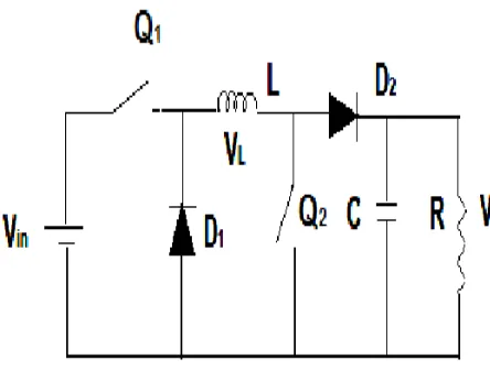
The two-switch buck-boost (TSBB) converter, as shown in fig. 4, is a cascade connection of simple buck and boost converters [9]-[12]. There are two active switches in the TSBB converter, QI and Q2 which are switched ON and OFF depending on the input voltage.
Fig.5. Schematic diagram ofTSBB
Fig 6 (c) Q. and Q2 are 'on' for boost mode (d) Q. 'on' and Q, is 'off' for boost mode
The voltage conversion of the TSBB converter operated in continuous current mode (CCM) [3].
V0 =d1/1-d2Vin
(1) where dl and d2 are the duty cycles of switches QI and Q2 respectively. When the input voltage goes higher, the TSBB converter operates in buck mode, where d2 = 0, then Q2 is always OFF, and dl is controlled so as to maintain the output voltage constant; when the input voltage goes lower, the TSBB converter operates in boost mode, where dl = 1, then QI is always ON, and d2 is controlled to regulate the output voltage. Thus, the voltage conversion of the TSBB converter with twomode control scheme can be written as [10]
Vo=(d1 vin,d2=0(vin>/vo)----
(2) IV. MODES OF OPERATION OF TSSB
Fig. 5 (a), (b), (c) and (d) gives the different modes of operation TSBB when the switch QI and Q2 are operated.
When input is higher than the output TSBB operates as a simple buck converter, then Q2 is permanently 'off and QI will be switching.
(a) When QI is 'on' then the input supplies the load and charges the capacitor. Since the input also charges the inductor, the current flow to the load is restricted and there is only a gradual build up. Also diode DI is reverse biased and D2 is forward biased.
(b) When QI is kept 'off, DI is forward biased and the stored energy in the inductor discharges and once the stored energy in inductor falls down, the capacitor begins to supply the load.
Mode II:
When input is lower than the output TSBB operates as a simple boost converter, then QI is permanently 'on' and Q2 will be switching.
(c) When Q2 is 'on' the input charges the inductor. The capacitor which is charged in the previous cycle supplies the output. Both the diodes D, and D2 are reverse biased.
(d) When Q2 is kept 'off, D, is reverse biased and the stored energy in the inductor discharges. This charge along with the input will feed the load and charge the capacitor.
V DESIGN OF Two SWITCH BUCK BOOST CONVERTER:
The Two Switch Buck Boost converter is designed for CCM mode depending on the input voltages, output voltage and power. The input voltage variation is from (2IOV-250V) for an output of 220V, lkW. The design steps are given as follows:
(3) Where VD represents diode voltage, YOU! and Yin represents the input and output voltage respectively.
The inductor and capacitor design is as,
(4)
(5)
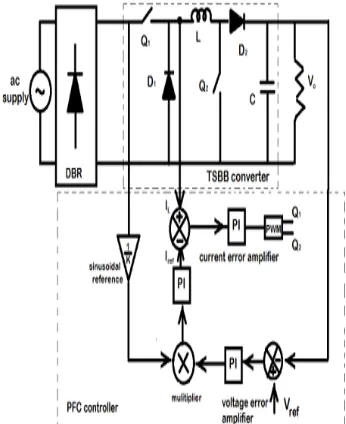
VI TSBB ALONG WITH POWER FACTOR CORRECTION CIRCUIT
Fig. 6 shows a two switch buck boost converter
An outer control loop for voltage correction and an inner feed forward control loop for power factor correction. The output voltage is compared with the reference voltage, the error thus obtained is multiplied with a unit input voltage so that the error voltage follows the shape of the input voltage. The output is then compared with inductor current and the error compared with the required saw tooth waveform to give necessary pulses to each switch. If output voltage is higher than reference voltage it goes to buck mode, when output voltage is lower than reference voltage then they operate in boost mode [13]-[16].
Fig.7. Schematic diagram of TSBB with PFC
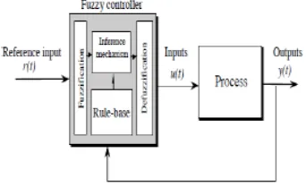
VII INTRODUCTIONTOFUZZYLOGIC
CONTROLLER
L. A. Zadeh presented the first paper on fuzzy set theory in 1965. Since then, a new language was developed to describe the fuzzy properties of reality, which are very difficult and sometime even impossible to be described using conventional methods. Fuzzy set theory has been widely used in the control area with some application to dc-to-dc converter system. A simple fuzzy logic control is built up by a group of rules based on the human
knowledge of system behavior. Matlab/Simulink
converts input data into suitable linguistic values; a knowledge base, which consists of a data base with the necessary linguistic definitions and the control rule set; a decision-making logic which, simulating a human decision process, infer the fuzzy control action from the knowledge of the control rules and linguistic variable definitions; a de-fuzzification interface which yields non fuzzy control action from an inferred fuzzy control action [10].
Fig.5. General Structure of the fuzzy logic controller on closed-loop system
The fuzzy control systems are based on expert knowledge that converts the human linguistic concepts into an automatic control strategy without any complicated mathematical model [10]. Simulation is performed in buck converter to verify the proposed fuzzy logic controllers.
Fig.6. Block diagram of the Fuzzy Logic Controller (FLC) for dc-dc converters
A. Fuzzy Logic Membership Functions:
The dc-dc converter is a nonlinear function of the duty cycle because of the small signal model and its control method was applied to the control of boost converters. Fuzzy controllers do not require an exact mathematical model. Instead, they are designed based on general knowledge of the plant. Fuzzy controllers are designed to adapt to varying operating points. Fuzzy Logic Controller is designed to control the output of boost dc-dc converter using Mamdani style fuzzy inference system. Two input
variables, error (e) and change of error (de) are used in this fuzzy logic system. The single output variable (u) is duty cycle of PWM output.
Fig. 7.The Membership Function plots of error
Fig.8. The Membership Function plots of change error
Fig.9. the Membership Function plots of duty ratio
B. Fuzzy Logic Rules:
The objective of this dissertation is to control the output voltage of the boost converter. The error and change of error of the output voltage will be the inputs of fuzzy logic controller. These 2 inputs are divided into five groups; NB: Negative Big, NS: Negative Small, ZO: Zero Area, PS: Positive small and PB: Positive Big and its parameter [10]. These fuzzy control rules for error and change of error can be referred in the table that is shown in Table II as per below:
Table II
VIII MATLAB/SIMULINK RESULTS
Fig 8 Matlab/simulation conventional circuit of TSBB without PFC
Fig 9 Matlab/simulation wave form of output voltage
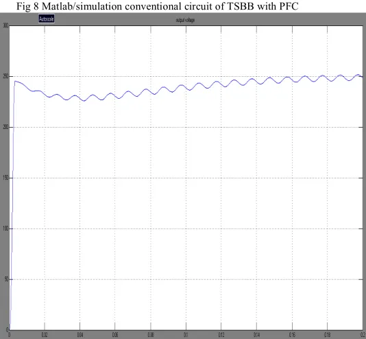
Fig 8 Matlab/simulation conventional circuit of TSBB with PFC
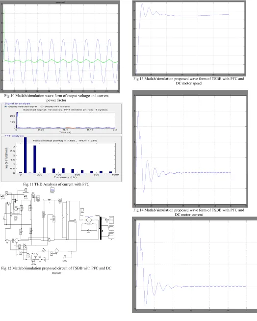
Fig 10 Matlab/simulation wave form of output voltage and current power factor
Fig 11 THD Analysis of current with PFC
Fig 12 Matlab/simulation proposed circuit of TSBB with PFC and DC motor
Fig 13 Matlab/simulation proposed wave form of TSBB with PFC and DC motor speed
Fig 15 Matlab/simulation proposed wave form of TSBB with PFC and DC motor torque
CONCLUSION
Widespread use of power electronics loads has given more attention to power factor correction (PFC) and reduction in harmonic distortion in the current drawn from the electric power utility. Various power factor correction (PFC) techniques such as buck converter boost converter, buck boost converter topologies are employed to overcome the power quality problems. This paper proposes a Two Switch Buck Boost converter along with a power factor correction control to improve the power factor and hence reduce the THD. The Two Switch Buck Boost Converter has the advantage of reduced switching losses. Study on DC motor drive has been done and an average current mode controller which was found to be more effective has been selected. Simulation of the converter with and without PFC controller has been performed in MATLAB/Simulink. Using this controller power factor correction and voltage regulation were achieved with single stage.
REFERENCES
[1] C. A. Heger, P. K. Sen and A. Morroni, "Power Factor correction-A fresh look into Today's Electrical Systems, " IEEE, 2012.
[2] C. Yao, X. Ruan, W. Cao, and P. Chen, "A Two-Mode Control Scheme With Input Voltage Feed-Forward for the Two-Switch Buck-Boost DC-DC Converter, " IEEE Trans. Power Electron., vol. 29, no. 4, pp. 2037-2048, April 2014.
[3] N. G. Hingorani, L. Gyugi, "Undersanding FACTS, Concepts and Technology of Flexible AC Transmission Systems ".
[4] 0. Garcia, 1.A. Cobos, R. Prieto, P. Alou and 1. Uceda, "Power factor correction: a survey, " in IEEE 32nd Power Electronics Specialists Conference (PESC), 2001, vol. 1, pp. 8-13.
[5] A. Fernandez, 1. Sebastian, P. Villegas, M. M. Hernando and D. G. Lamar, "Dynamic limits of a power-factor preregulator, " IEEETransactions on Industrial Electronics, vol. 52, no. 1, pp. 77- 87, Feb. 2005.
[6] P. N. Ekemezie, "Design Of A Power Factor Correction AC-DC Converter, " IEEE Conference Publications [Accessed March 10, 2010].
[7] Prof. Chi K. Tse, "Circuit Theory and Design of Power Factor Correction Power Supplies, " IEEE Distinguished Lecture 2005, Circuits and Systems. [8] A. Karaarslan, I. Iskender, "The analysis of ac-dc boost PFC converter based on peak and hysteresis current control techniques, " International Journal on Technical and Physical Problems of Engineering (IJTPE), Iss. 7,
Vol. 3, No. 2, pp. 100-105 Jun. 2011.
[9] C. Yao, X. Ruan, and X.Wang, "Isolated buck-boost dc/dc converters suitable for wide input-voltage range, " IEEETrans. Power Electron., vol. 26, no. 9, pp. 2599- 2613, Sep. 2011.
[10] B. Singh, B. N. Singh, A. Chandra, K. AI-Haddad, A. Pandey, and D. P. Kothari, "A review of single phase improved power quality AC DC converters, " IEEE Trans. Ind. Electron., vol. 50, no. 5, pp. 962-981,Oct. 2003.
[11] R. W. Erickson and D. Maksimovic, Fundamentals of Power Electronics. Norwell, MA, USA: Kluwer, 2011. [12] C. Spiazzi, P. Mattavelli, L. Rossetto, "Power Factor Pre-Regulators with Improved dynamic Response, " IEEE Transactions on Power Electronics, Vol. 12, Issue 2, pp. 343-349, March 1997.
[13] W. P. Zhang, F. Chen, X. S. Zhao and Y. C. Liu, "A Discrete Modeling for Power Factor Correction Circuit, " PEDS 2009, pp. 160-163.
[14] K. De Gusseme, D. M. Van de Sype, A. P. M. Van den Bossche, and 1. A. Melkebeek, "Digitally controlled boost power-factor- correction converters operating in both continuous and discontinuous conduction mode, " IEEETrans. Ind. Electron., vol. 52, no. 1, pp. 88-97, Feb. 2005.
[15] G. K. Andersen and F. Blaabjerg, "Current programmed control of a single-phase two- switch buck-boost power factor correction circuit, " IEEETrans. Power Electron., vol. 53, no. 1, pp. 263-271, Feb. 2006.