Design and Simulation of Eight Point FFT Using VHDL and MATLAB
1
Anant G. Kulkarni,
2Dr. Manoj Jha,
3Dr. M. F. Qureshi
1
Research scholar, Dr. C. V. Raman University, Bilaspur, India,
2
Department of Mathematics, Rungta Engineering College, Raipur, India,
3
Department of Electrical Engineering, Government Polytechnic, Dhamtari, India,
Abstract: The FFT are widely used in various
areas such as telecommunications (radio communications links and telephone networks), speech and image processing, medical electronic and voice signal processing and data acquisition[1].This paper concentrates on developing Fast Fourier Transform (FFT). Based on Decimation-In- Frequency (DIF) Radix-2 algorithm and 8-points computation, this paper used VHDL as a design entry [6]. This paper gives a better idea to implement FFT algorithm using VHDL for behavior modeling and compare result with Mat lab.
1. Introduction: In last few years many
researchers have attempted to develop FFT processor to calculate N point FFT. Almost all the researchers have adopted structural method to implement FFT algorithm [3]. Problem in structural implementation of FFT was, it requires designing more number of components, although it is easier to design the basic components such as adders sub tractors to perform addition and subtraction operation, shift register of different bit length to store the result at different stages, multiplier to multiply twiddle factor which is a complex number but due to large no of components complexity of the circuit was increased. Now another problem in structural implementation of FFT was to interconnect all the components to produce the correct output to calculate N point FFT.
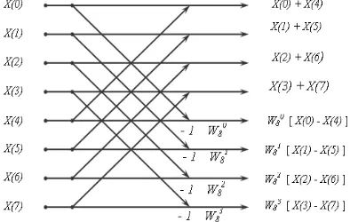
2. Structural Implementation In structural
implementation of FFT, the single butterfly computation is implemented in the data path unit. A control unit controlling the data path and determine the stage of operations. The control unit coordinates the appropriate pairs of inputs into the butterfly computation and the output
pairs is store in the memory. Each pair of random input bits will undergo multiples of butterfly computation in stage 1. Assume the input string bits are x0, x1, x2, x3, x4, x5, x6, and x7 respectively[3].
Stage 1 computation will pairs up input bits to x(0) - x(4), x(2) - x(6), x(1) - x(5) and x (3) - x (7). Stage 1 computation will store its result in certain memory location; assume memory A. At stage 2, the result in memory A is feed into butterfly computation in pairs. The control unit acts as a selector to select the correct input for the butterfly input for the butterfly computation in every stage. The output from Stage 2 is stored in the same memory location. For 8-point FFT, the process ends at Stage 3. The final output is the computed Fast Fourier Transform [5].
Stage 1 Stage 2 Stage 3
Memory Memory Location A Location A
3. Direct Mathematical Method of 8-point
FFT
:In direct mathematical approach, the
final output is derived from the input
mathematically. The explanation is based on
three stages in the 8-points FFT with assumption that only real binary bits as an input. Stage 1 deals with raw input samples directly, with each of these samples contain a string of 16-bits input. In the Figure 1. It is shown that there are 3 stages in an 8-point FFT. Stage1 accepts the input data directly. The Figure 2 shows the computation of Stage 1.So, at the input of first stage, there are 8 points x 16 bits = 128 bits.
Fig. 2 Computation of Stage 1
It is shown the even samples and odd samples are processed separately. The outputs of Stage 1 are feed as the inputs of the Stage 2. Stage 2 computation take place and this process repeats at the final stage, Stage 3.The output of Stage 1 will be as an input of Stage 2. The complexity of the output equations increases as the stage number increases because twiddle factor computations are involved. The twiddle factor includes multiplication and additions operations. Figure 3 shows the stage 2 computation. The even inputs are grouped together and summed up in pairs. The other inputs are multiplied with their respective twiddle factor. Each of these inputs will undergo butterfly operation. Some of the output will have to multiply again with the twiddle factor.
Fig. 3 Computation of Stage 2
The outputs of the Stage 2 will be an input of Stage 3. At Stage 3, the butterfly computations are repeated. The computations are increased.
Fig. 4 Computation of Stage 3
8 Point FFT:
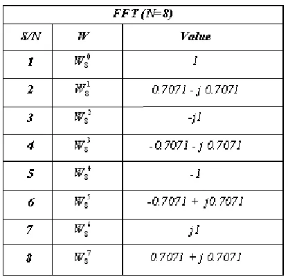
Table 1: Twiddle Factor value for FFT
The final equations have been optimized for an efficient implementation. The twiddle
factors
are represented by 16 bit binary number. Final equations for an 8-point FFT processor:
X (0) = x (0) + x (4) + x (2) + x (6) + x (1) + x (5) + x (3) + x (7)
X (1) = x (0) – x (4) – j x (2) + j x (6) + 0.7071 x (1) – j 0.7071 x (1) – 0.7071 x (5)+ j 0.7071 x (5) - 0.7071 x (3) – j 0.7071 x (3) + 0.7071 x (7) + j 0.7071 x (7) X (2) = x (0) + x (4) – x (2) – x (6) – j x (1) – j x
(5) + j x (3) + j x (7)
X (3) = x (0) – x (4) + j x (2) – j x (6) - 0.7071 x (1) – j 0.7071 x (1) – 0.7071 x (5) + j 0.7071 x (5) + 0.7071 x (3) + j 0.7071 x (3) - 0.7071 x (7) – j 0.7071 x (7)
X (4) = x (0) + x (4) + x (2) + x (6) – x (1) – x (5) – x (3) – x (7)
X (5) = x (0) – x (4) – j x (2) + j x (6) + 0.7071 x (1) – j 0.7071 x (1) - 0.7071 x (5)
+ j 0.7071 x (5) - 0.7071 x (3) – j 0.7071 x (3) + 0.7071 x (7) + j 0.7071 x (7)
X (6) = x (0) + x (4) – x (2) – x (6) – j x (1) – j x (5) + j x (3) + j x (7)
X (7) = x (0) – x (4) + j x (2) – j x (6) + 0.7071 x (1) + j 0.7071 x (1) - 0.7071 x (5) - j 0.7071 x (5) + 0.7071 x (3) + j 0.7071 x
(3) - 0.7071 x (7) – j 0.7071 x (7)
4. Proposed System: The implementation of an
8 point FFT processor involved few modules. All this module are combined together to produce an 8 point FFT processor. Figure 5 shows the complete functional block diagram where the inputs are passed into the design synchronously at every positive edge triggered. Then, the path module shows the arithmetic computation for each respective output. In the FFT algorithm (generally), the even and odd outputs are computed separately in two main groups. The odd output blocks computation is more complex compared to the even group computation. The odd output computations are represented by Path 1, Path 3, Path 5 and Path 7. The even output computations are Path 0, Path2, Path 4 and Path 6. In the even outputs, the twiddle factor at the output equations has been simplified.
Fig. 5 Block diagram of an 8 point FFT
processor
Pass module of FFT processor: This module is
to pass the input data at each positive clock edge to the different modules of FFT processor. The pass module consists of 8 D flip-flop registers[7]. The outputs of this block are 8 lines of 16 bit output which are connected to Path 0, Path 1, Path 2, Path 3, Path 4, Path 5, Path 6 and Path 7. One clock signal is required to pass the data in.
Path 0 and Path 4 module of FFT processor The outputs of Path 0 and Path 4 are Xout (0)
(4) arithmetic involves summation and subtraction. There is no imaginary component present at the output.
Path 2 and Path 6 module of FFT processor:
The outputs of Path 2 and Path 6 are Xout (2) and Xout (6) respectively. The arithmetic operation for Xout (2) and Xout (6) involves real and imaginary operation. They are performed separately. The arithmetic operation involves summation and subtraction. The twiddle factor for this output is –j which contributes to the imaginary component for this path. Thus, Path 2 and Path 6 have more complex mathematical expressions.
Path 1, Path 3, Path 5, Path 7 modules of FFT processor: The outputs of Path 1, Path 3, Path 5 and Path 7 are Xout (1), Xout(3), Xout(5) and Xout(7) respectively. The arithmetic operations for all of these modules involve real and imaginary operation. They are performed separately.
The twiddle factor for all these modules consists of real an imaginary value of sine 45 degree or cos 45 degrees. The output of the twiddle factor is approximated to 0.7071[5]. In this design, the value is approximated to 0.707092285 or in binary 0.01011010100000100, including a most significant bit (MSB) to indicate the twiddle factor is a positive number[8]. Any decimal value after summation is approximate to integer ‘1’ when it is greater than 0.5. These blocks are the most complicated among all the modules in the FFT processors because it involves a number of Mathematical operators, like addition, subtraction and multiplication.
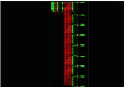
5.Simulated output: This section shows the
overall simulation result obtained by combining all the modules that has been presented earlier.
Figure 6 Simulated result of complete
module.
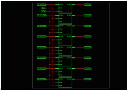
Figure 7 RTL schematic of complete FFT
module.
Figure 9 Internal blocks of Pass M module.
Figure 10 Example of 8-point FFT
Figure 10 Result of 8-point FFT using MATLAB
6. Conclusion Direct mathematical method is
adopted because it is an efficient and optimized method instead of the structural implementation which is based on butterfly operation .The timing simulation is performed from VHDL. The results were tested using conventional method. From the result shown in the results chapter, FFT module was correctly operated. The difference was only that the result
of the FFT computation was in decimal while conventional method provide in floating point value. Figure 10 shows result of 8-point FFT using Matlab.
In conclusion, the main objective of this project has been successfully accomplished and the result obtained from this work is verified.
Table 2 Comparison of memory between
Structural and Mathematical Implementation
Scope of future Work Although the objectives
of the thesis have been attained, there are a few fundamental directions that present themselves for continued research:
First, this design can be modified to accept complex number. Additional digital circuitry implementation can be performed such that this design can accept complex number as inputs.
Use higher fixes point representation for point value representation. In real time applications and system that required high precision and high speed, 8 points computation is not suitable. Therefore the higher N-points should be design to comply this need.
References:
[1] Huang ping,Zu Bing-fa, Wang Hui“Pseudo Noise Code Acquisition Using Fast Fourier.Transform”.InternationalSymposi-um on Computer Science and Computational Technology. Page No. 788-791. May 2008.
[2] Wei Han, Ahmet T. Erdogan, Tughrul Arslan, and Mohd. Hasan “High-PerformanceLow-Power FFT Cores”. ETRI Journal, Volume 30, Number 3, page 451-460,June 2008. [3] Yuke Wang , Yiyan Tang ,Yingtao Jiang,
Jin-Gyun, Sang-Seob Song, Myoung-Seob “Novel Memory Reference Reduction Methods for FFT Implementations on DSP Processors”. IEEE TRANSACTIONS ON SIGNAL PROCESSING, VOL. 55, NO. 5, page 2338-2349, MAY 2007.
[4] John G. Proakis and D. G. Manolakis, “Digital Signal Processing: Principles, Algorithms and Applications”, New York: Macmillan Publishing Company, Second Edition, 1992, chapter -6, page 456-464. [5] S.salivahan, A Vallavraj and C. Gnanapriya
“ Digital Signal Processing” New Delhi Tata
McGraw-Hill Publishing Company Limited. Nineteenth edition 2006, chapter -6, page 319-350
[6] J.Bhaskar “A VHDL Primer” Pearson Printice Hall Publication Third Edition 2007. [7] Stephen Brown and Zvonko Vranesic
“ Fundamentals of Digital Logic Design with VHDL. Tata McGraw-Hill Publishing Company Limited. Second Edition 2007.
[8] David Elam and Cesar Iovescu. “A Block
Floating Point Implementation for an N-Point FFT on the TMS320C55x DSP”. Application Report , SPRA948 page1-11 Sep. 2003.
[9] Anant G. Kulkarni & Sudha Nair “Design and Implementation of Frequency Analyser using VHDL”, International Journal of Electronics Engineering , Volume 1, Number 2, pp. 265-268, July-December 2009, ISSN: 0973-7383.
[10] Pradeep K. Jaisal, Anant G. Kulkarni and Shrikant B. Burje, “Design and Simulation of 8255 Programmable Peripheral Interface Adapter Using VHDL”, International Journal of Computer Science and Technology,
Vol 2, Issue 1, pp. 178-181, March 2011, ISSN: 2229-4333(Print), ISSN: 0976-8491(Online).