ISSN (Print) : 2320 – 3765 ISSN (Online): 2278 – 8875
I
nternational
J
ournal of
A
dvanced
R
esearch in
E
lectrical,
E
lectronics and
I
nstrumentation
E
ngineering
(An ISO 3297: 2007 Certified Organization)
Vol. 5, Issue 9, September 2016
Single-Inductor Multiple-Output Buck–Boost
Power Factor Correction Converter
Sangeetha Merin Sunny 1, Liju Mathew R 2
P.G. Student, Department of EEE, St. Joseph’s College of Engineering & Technology, Palai, Kerala, India1
Associate Professor, Department of EEE, St. Joseph’s College of Engineering & Technology, Palai, Kerala, India2
ABSTRACT: A single-inductor multi-output (SIMO) buck boost power factor correction (PFC) converter working under critical conduction mode is proposed here.Different output voltages can be generated with the help of this converter. Only one inductor is required.Compared with a conventional two stage multiple output converter,the SIMO converter benefits from significant over-all cost saving, small size, and light weight By multiplexing a single inductor, each output of the buck boost converter can be regulated independently.Moreover, the effciency of the SIDO buck boost PFC converter can be improved due to single-stage power conversion. These converters are the most efficient and cost effective solution for multiple output power supplies.
KEYWORDS:power factor correction, multiplexing , buck-boost Converter..
I. INTRODUCTION
Multiple-output ac/dc power converter has been becoming popular in recent times. In order to achieve a high PF and to accurately regulate the output voltages or currents of a multiple-output ac/dc converter,a conventional multiple-output ac/dc power converter consisting of two-stage power conversion is utilized.The SIMO converters has many advantages over the conventional two-stage multiple-output converter, such as they benefits from smallsize,light weight and significant overall cost saving.The concept single inductor multiple output converters arise inorder to overcome ihe dis advantages of conventional converters such as complex and suffers from high cost, with multiple inductors and controllers required.The SIMO topology capable of generating independently controlled buck, boost, and inverted (buck/boost) outputs simultaneously
.
[2]A control scheme is developed for Reduced Cross-Regulation in Single-Inductor Multiple-Output DC-DC Converters. SIMO converters with its advantages in implementation suffer from instability in system dynamics due to the coupled outputs.This control scheme ensures stable system performance in both steady state and transient with good line and load regulation but also reduces (close to zero) cross-regulation at the outputs[3]. For a multiple-output converter with each output regulated independently, if one output is affected by the variation of other outputs, transient cross-regulation occurs.
The work done in this paper is divided in two stages. 1) Power Stage 2) Implementation.In the Power Stage of the SIMO converter includes the analysis of the converter is done.software used here is Matlab Simulink.Hardware and Simulation results are described in the following sections.
This paper is organized as follows. In Section II, the SIMO buck–boost PFC converter is proposed and analyzed. The design considerations and Matlab simulations are described in Section III. The experimental results are given in Section IV, and Section V summarizes the conclusion drawn from the study.
II. SYSTEMMODEL
Fig 1. SIDO buckboost PFC converter.
The power stage of the SIDO buck boost PFC converter consists of a diode bridge Dbridge.An input filter consisting of Lf and Cf. Three switch networks consisting of Q1, Q2 and Q3 and their corresponding sense resistors Rs1, Rs2,and
Rs3,two freewheeling diodes D1 and D2,a time-multiplexing inductor L,and two output filter capacitors C1 and C2
.Time-multiplexing control switches of each output are Q2 and Q3.When Q2 is turned on and Q3 is turned off, the converter
transfers power to output A, and when Q2 is turned off and Q3 is turned on, the converter transfers power to output B.In
the above converter applications are limited upto two voltages.Hence the idea of multiple output converters where obtained in which different output voltages can be generated from the same input voltage.They are used for multiple output power supplies.Figure below shows the circuit diagram of a SIMO converter.
Fig 2. Proposed SIMO buckboost PFC converter.
The power stage of the SIMO buck-boost converter consists of a diode bridge Dbridge; an input filter consisting of Lf
and Cf ; five switch networks consisting of Q1,Q2,Q3,Q4,and Q5and their corresponding sense resistors Rs1,Rs2 , and
Rs3;four freewheeling diodes D1, D2, D3,and D4; a time multiplexing inductor L; and three output filter capacitors C1,
C2, and C3. Q2,Q3,Q4, and Q5 are the time multiplexing control switches of each output. The switch Q1 is always in on
ISSN (Print) : 2320 – 3765 ISSN (Online): 2278 – 8875
I
nternational
J
ournal of
A
dvanced
R
esearch in
E
lectrical,
E
lectronics and
I
nstrumentation
E
ngineering
(An ISO 3297: 2007 Certified Organization)
Vol. 5, Issue 9, September 2016
off and Q3 is turned on, the converter transfers power to output A. For the third output the switch Q4 is turned on and
Q5 is turned off that time the capacitor C stores the charge .After charging the capacitor the switch Q4 is turned off and
the switch Q5is turned on, the converter transfers power to the output C.
III.DESIGNCONSIDERATIONANDMATLABSIMULATIONS
The analysis of the SIMO converter is done under the following assumptions: 1) All the components are ideal
2) Switching frequency is higher than the line frequency.
3) Input voltage is a rectified sine wave, that is Vin,rec(t)=|vin(t)|=Vp|sin(WLt)|,where Vp is the amplitude of the
sine wave.
4) The output voltages Voa ,Vob and Voc are constant ,they have ac ripple in the steady state.
5) The bandwidth of the PFC converter in the control loop is usually much lower than the rectified line frequency. 6) The error voltage of three output is constant within each half of the line cycle.
By using MATLAB Fig shows the PF of the SITO buckboost PFC converter,its shows that by increase the value of k, power factor will be close to 1.The value of k is determined by k1,k2and α.Let λ=α2 and it is defined as the power ratio
of Po,A,Po,B and Po,C by using MATLAB,The relationship of PF ,k1,k2 and λ ..PF will be seriously affected when λ
increases.It clearly tells that k1 is equal to k2.
Fig.4. Output voltage(Vin=240)
Output voltage is same for two different input voltages. multiple output voltages are produced by the SIMO converter since they are used for multiple output power supplies.Two input voltages voltages are given here.output voltage is constant for different input voltages.
ISSN (Print) : 2320 – 3765 ISSN (Online): 2278 – 8875
I
nternational
J
ournal of
A
dvanced
R
esearch in
E
lectrical,
E
lectronics and
I
nstrumentation
E
ngineering
(An ISO 3297: 2007 Certified Organization)
Vol. 5, Issue 9, September 2016
Fig. 6 Input voltage and current waveform
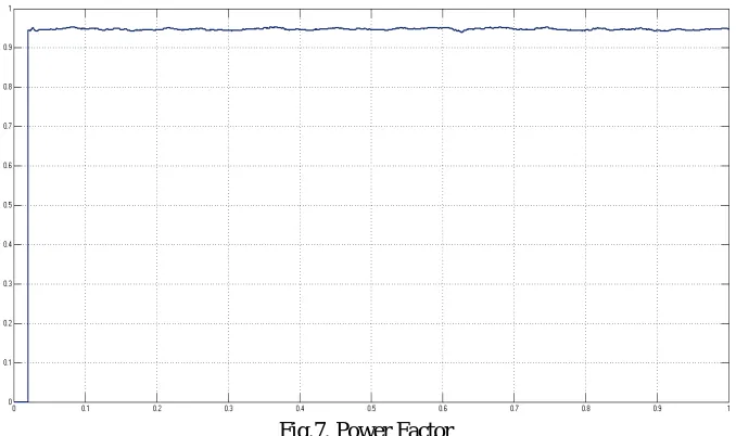
Power factor correction is possible in SIMO converter since input voltage and current are in phase as shown in fig 6.here,input current is marked in rose colour while input voltage is marked in blue,power factor is shown as in fig 7.it is less than one.
Fig.7. Power Factor
IV.EXPERIMENTAL RESULTS
The prototype of the proposed SIMO buckboost PFC shown in Fig.8 is built to verify the theoretical analysis.Each output current Of the proposed SIMO buck-boost PFC is constant.The prototype parameters of SIMO are shown in Table I.The voltage is varying from 100 to 240 Vac .According to the analysis L is designed as 180µH.Lf and Cf are
the size of the filter. Here Lf and Cf are filter.Here Lf and Cf are .designed as 1mH and 220nF considering a wide input
voltage
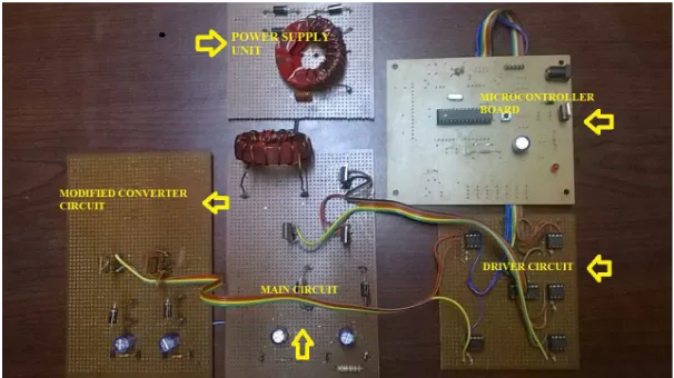
Circuit parameter of the proposed converter is shown here.different parameters are written here.overall hardware setup is described as follows which consist of power supply unit, microcontroller board,driver board,modified converter circuit etc.
Fig.8. Overall Hardware setup
VARIABLE DEFINITION VALUE
VIN INPUT VOLTAGE 100-240V
R LOAD RESISTOR 300
IA CURRENT OF OUTPUT
A
0.2
IB CURRENT OF OUTPUT
A
0.25
VOA VOLTAGE OF OUTPUT
A
60
VOB VOLTAGE OF OUTPUT
B
75
LF INPUT FI LTOR
INDUCTOR
1ΜH
ISSN (Print) : 2320 – 3765 ISSN (Online): 2278 – 8875
I
nternational
J
ournal of
A
dvanced
R
esearch in
E
lectrical,
E
lectronics and
I
nstrumentation
E
ngineering
(An ISO 3297: 2007 Certified Organization)
Vol. 5, Issue 9, September 2016
Fig.9. Output Voltage waveform
The output waveform for the proposed converter shown here and it is verified experimentally.
V.CONCLUSION
A single inductor multi output buck boost power factor correction conveter is proposed here.From the input and output voltage current waveforms,it is clear that the proposed converter is used for power factor correction.since,PFC is usually used to provide a sinusoidal input current. The proposed converter is also act as a voltage regulator since it maintains a constant voltage level.For a varying input voltage,value of output voltage and current is constant.Buck boost operation is possible because one output voltage is greater than input voltage.Di_erent number of output voltages can be generated from same converter which makes it more cost saving, small size, and light weight.Experimental results have been presented to verify the analysis results and to demonstrate the advantage of the proposed converter.
REFERENCES
[1] Taesik Park,and Taehyung Kim,"Single-Inductor Dual-Output BuckBoost Power Factor Correction Converter",IEEE Trans.PE, vol. 28, no. 1, Jan. 2013.
[2] Y.-J. Lee, A. Khaligh, and A. Emadi,"Advanced integrated bidirectional AC/DC and DC/DC converter for plug-in hybrid electric vehicles",IEEE Trans.PE,vol.58,no.8,pp.3970-3980,Oct.2009.
[3] F. Musavi, M. Edington, W. Eberle, and W. G. Dunford, "Control loop design for a PFC boost converter with ripple steering,"IEEE Trans. on. PE.,vol.49,no.1,pp.118-126,Jan./Feb.2013.
[4] J. Cao and A. Emadi, "A new battery/ultra capacitor hybrid energy stor-age system for electric, hybrid, and plug-in hybrid electric vehicles, ,IEEE Trans.PE,vol.27,no.1,pp.122-132,Jan.2012.
[5] D. Ma,W.-H. Ki, and C.-Y. Tsui,"A pseudo-CCM/DCM SIMO switching con-verter with freewheel switching,"IEEE Trans.PE,vol.38, no.6,pp.1007-1014,Jun.2003.
[6] P. Patra, J. Ghosh, and A. Patra,"Control scheme for reduced crossreg-ulation in single-inductor multiple-output dc-dc converters,"IEEE Trans.PE vol.60,no.11,pp.5095-5104,Nov. 2013
[7] C. K. Tse,M. H. L. Chow, andM. K. H. Cheung,"A family of PFC voltage regulator con_gurations with reduced redundant power processing,"IEEE Trans.PE,vol.16,no.6,pp.794-802,Nov.2001.
[8] F. Musavi, M. Edington, W. Eberle, and W. G. Dunford, "Control loop design for a PFC boost converter with ripple steering,"IEEE Trans. on. PE.,vol.49,no.1,pp.118-126,Jan./Feb.2013.
[9] D. Ma, W.-H. Ki, C.-Y. Tsui, and P. K. T. Mok, “Single inductor multiple output switching converters with time-multiplexing control in discontinuous conduction mode,” IEEE J. Solid- State Circuits, vol. 38, no. 1,pp. 89–100, Jan. 2003.
[10] J. Cardesín, J. Ribas, E. López Corominas, and M. A. Dalla Costa, “LED permanent emergency lighting system based on a single magnetic component,”IEEE Trans. Power Electron., vol. 24, no. 5, pp. 1409–1416,May 2009.
[11] V. Vlatkovic, D. Borojevic, and F. C. Lee, “Input filter design for power factor correction circuits,” IEEE Trans. Power Electron., vol. 11, no.1,pp. 199–205, Jan. 1996