Performance Evaluation of Advanced
Three-Level AC– DC Converter Fed Induction Machine Drive
P. Vijay Ravi ; T.Srinivasa Rao & K. Durga Rao
1
M-Tech Student Scholar ;
2Associate Professor;
3Assistant Professor
Department of Electrical & Electronics Engineering, Avanthi Institute of Engineering and Technology,Makavarapalem,
Visakhapatnam
.
Abstract-
The topology of this converter is derived by
combining a boost circuit and a forward circuit in one
power stage. To improve the performance of the ac–dc
converter (i.e., good power factor correction, low total
harmonic distortion (THD) and low dc bus voltage),
two bulk storage capacitors are adopted. Its excellent
line regulation capability makes the converter suitable
for universal input application. The operation of the
converter is discussed in the project and its various
modes of operation are explained in detail. Two
independent controllers are majorly used to operate
the converter namely an input controller that performs
power factor correction and regulates the dc bus and
an output controller that regulates the output voltage.
They consist of an ac–dc boost pre regulator converter
that shapes the input current and an isolated dc–dc
full-bridge converter that converts the pre regulator
output into the required dc voltage.
Research on the
topic of higher power ac–dc single-stage full-bridge
converters, however, has proved to be more
challenging, and thus, there have been much fewer
publications.
They use passive elements such as
inductors and capacitors to filter low frequency input
current harmonics and make the input current more
sinusoidal. Two stage converters, however, require
two separate switch-mode converters (each with its
own controller), and thus, can be expensive.
Moreover, they have poor efficiency when operating
under light-load conditions as there are two converter
stages that are operating each with its own set of fixed
losses while a small amount of power is actually
transferred to the load. The converter is designed by
using
Induction
Drive
System
for
Irrigation
Applications Matlab/Simulink software.
Index
Terms—
Induction
Drive;
three-level
converters; Single-stage power factor correction
(SSPFC); AC–DC power conversion
I. INTRODUCTION
Recently, developments in power electronics and
semiconductor technology have lead improvements in power electronic systems. Pulse Width Modulation variable speed drives are increasingly applied in many new industrial applications that require superior performance. Hence, different circuit configurations namely inverters have become popular and considerable interest by researcher are given on them. Variable voltage and frequency supply to A.C drives is invariably obtained from a three-phase voltage source inverter. To overcome the limited semiconductor voltage and current ratings, some kind of series and/or parallel connection will be necessary. Due to their ability to synthesize waveforms with a better harmonic spectrum and attain higher voltages, multi-level inverters are receiving increasing attention in the past few years. THE ac–dc power
supplies with transformer isolation are typically
implemented with some sort of input power factor correction (PFC) to comply with harmonic standards such as IEC 1000-3-2 [1],[2].
With the rapid rise in the use of electrical equipment in recent years, power converter manufactures are being pressed by regulatory to implement some form of PFC in their products. High power factor and low input current harmonics are more and more becoming mandatory performance criteria for power converters. Although it is possible to satisfy by adding passive filter elements to the
traditional passive diode rectifiers/LC filter input
combination. The result of this converter is very bulky and heavy due to the size of the low frequency inductors and capacitors. Active power factor correction techniques have been used in AC-DC converter to improve power factor and reduce the harmonics. Active power factor correction can be classified into two stage scheme. Two stages PFC contain two independent power stages in cascade with PFC stage and DC-DC regulator[3].
its operating principles, various modes of operation and finally its features, design aspects.
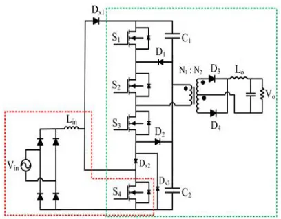
Fig.1. Proposed single-stage three-level converter.
The total efficiency of the two stages is lower because the total power has to be processed twice with two cascade power stage. Cost of the circuit is increase several schemes have developed to combine stage into one stage [4]. This paper introduces the new converter is interfaced to induction machine drive to check the performance of the drive characteristics and explains along with its basic operating principles.
II. OPERATION OF THE PROPOSED CONVERTER
The Fig. 1, shown above is the proposed converter which integrates the operation of an ac–dc boost PFC converter into a three-level dc–dc converter. An input diode bridge, boost Inductor Lin, boost diode Dx1, and switch S4, which is shared by the multilevel dc–dc section are the major components of the ac–dc boost section. When S4is off, it means that no more energy can be captured by the boost inductor. Here the input current flowing to the midpoint of capacitors C1 and C2 is prevented by the diode Dx2 and the conduction of diode Dx1 helps to transfer the energy stored in the boost inductor Lin to the dc bus capacitor. Diode Dx2 is being bypassed by Diode Dx3 and makes a path for circulating current. It is operated with two independent controllers although being a single converter. To regulate the voltage across the primary side dc-bus capacitors by sending appropriate gating signals to S4 and to perform PFC one of the controller is used[5],[6].
To regulate the output voltage by sending appropriate gating signals to S1to S4 the other controller is used. The main important aspect which is to be noted here is that the control of the input section is decoupled from thecontrol of the dc– dc section and thus can be designed separately., Here on the basis of S, the gating signal of S is depended, which is the
output of the input controller; and the generation of this signal is discussed in detail later in this paper. Since the switches S2 and S3 are each ON for half a switching cycle, but are never ON at the same time so the generation of gating signals is easier for them. Here Fig. 2 shows the typical converter waveforms and Fig. 3 shows equivalent circuit diagrams that show the converter’s modes of operation with the diode rectifier bridge output replaced by a rectified sinusoidal source. As the switching frequency is higher than the input line frequency, it is assumed that the supply voltage is constant within a switching cycle. Although there is no reason why the input current cannot be made to be continuous so it is also assumed that the input current is discontinuous, if this is what is desired[7]. The converter has the following modes of operation:
Fig. 2. Typical waveforms describing the modes of operation.
1) Mode 1 (t0 ≤t≤t1):
S1and S2. The positive voltage on the output side of transformer is given across Lo which makes current rising.
2) Mode 2 (t1 ≤t≤t2): During this mode, the output load is energized by the discharge of dc-bus capacitor C1 by making S1 and S2 still Turn ON and S3 turns ON and also the output voltage of the diode bridge rectifier is given across the input inductor Lin thereby inductor current rising.
3) Mode3 (t2 ≤t≤t3): In this mode, the switches S1 and S2 are still Turn ON and S3 turns ON. The output
load is energized by discharging of dc-bus capacitor C1. The output voltage of diode bridge rectifier is applied across input inductor Lin in order to make the inductor current which raises voltage applied across input inductor Lin thereby inductor current rising.
4) Mode 4 (t3 ≤t≤t4): During this mode, S1 andS2 are OFF and S4 is ON. The capacitorC2 is being charged by the current in the primary of the transformer through the body diode of S3 and Dx3.
5) Mode 5 (t4 ≤t≤t5): In this mode, S3 andS4 are ON. Energy flows into the load from capacitorC2 while the current flowing through input inductor Lin continues to rise.
6) Mode 6 (t5 ≤t≤t6): During this mode, S4 turns off. The diode Dx1 conducts current in input conductor to charge the capacitors C1 andC2. Here S3 andD2 conducts current in the transformer primary winding. This mode ends when the inductor current reaches zero. The load inductor current freewheels in the secondary of the transformer in this mode.
8) Mode 8 (t7 ≤t≤t8): During this mode, S3 is OFF and the capacitor C1charges through the current in the primary of the transformer through the body diodes of S1 andS2. Finally, converter reenters Mode 1.
The Fig.4 shows the simplified schematic of the power converter and the respective controllers. Since the Cross over frequencies of the two loops is very different the decoupling of the input controller and output controller can occur. The input power factor correction and conversion of input ac into an intermediate dc-bus voltage due to the cross over frequency of the input controller, intermediate dc-bus voltage (voltage across the two primary side dc-bus capacitors), is much lower than that of the output controller, which converts the intermediate dc-bus voltage into the desired output voltage. It is possible to consider the design of one controller to be separate from that of the other, since the two crossover frequencies are far apart [8],[9].
The standard designs for a dc–dc full-bridge converter controller and an ac–dc boost converter controller can be used, since the two controllers are decoupled. The simple diagram of the controller scheme that has two elements of control is shown in
the Fig. 4. By controlling the gating signals of S1 to
S4 through controlling duty cycle of D1 the control of dc–dc conversion of the dc-bus voltage to the desired output voltage can be done and this will be the primary aspect to be noted. The secondary aspect which to be noted is to control duty cycle of the switch S4 to regulate the dc-bus voltage and to perform input power factor correction. This can be done by controlling D2 and then adding duty cycle of D2 to D1 (where D1 andD2 are defined in Fig. 2); thus S4 performs majorly two tasks; one part (D1) participate to control output voltage and another part (D2) to regulate dc-bus voltage.
III.CONVERTER FEATURES The proposed converter has the following features:
A) Reduced cost compared to two-stage converters:
The converter proposed in this paper may seem expensive but in practical terms it is much cheaper when compared to a conventional two-stage converter. The cost of the converter is low because replacing a switch and its associated gate drive circuitry with four diodes reduces cost considerably even though the component count seems to be increased and this is more real if the diodes are ordered in bulk numbers.
B) Better performance than a single-stage converter:
When compared to a single-stage single-controller, this single-stage converter can operate with a better input power factor for universal input line applications because it does have a dedicated controller for its input section that can regulate the dc-bus voltage and perform PFC. The converter can be made to operate with better efficiency and with less output ripple due to the presence of a second controller as each section can be made to operate in a optimal manner of the converter.
C) Improved Light-Load Efficiency:
D) Increased Design Flexibility:
The proposed converter can be operated with standard bus voltage (400 V), high bus voltage (800 V), or any dc-bus voltage 400 V<Vbus<800 V since the converter is a multi-level converter. While operating with high dc-bus voltage or with standard dc bus voltage the advantages are more often. The fact there is flexibility in the level that the dc-bus voltage is set means that there is considerable flexibility in the design of the converter. The design of the converter for other factors such as efficiency profile and cost (i.e. cost of switches based on voltage rating considerations and availability) can be optimized as per the designer’s options. The design of the three-level converter to be much simpler than that of a single-stage two-level converter or that of a single-controller three-level single stage converter as the dc-bus voltage can be fixed to a desired level that is considered appropriate can be made flexibly which is to be noted. It also has the advantage of
lower heavy-load efficiency because of increased
conduction losses as switch S4 must conduct both the input current and the full-bridge current which is an additional advantage over the aforementioned advantages over the conventional two-stage converter, which is to be noted. Hence various factors which include lower cost and improved light-load efficiency versus heavy-load efficiency are to be considered when determining whether to use the proposed converter versus a conventional two stage converter[10].
IV. MATLAB/SIMULINK RESULTS
Case i) Single phase single stage power factor corrected converter for three level
Fig.5: Matlab/Simulink Model of Single-Stage Three-Level Converter using Matlab/Simulink Software Package.
Fig.6: Input Current and Voltage Wave Form
Fig.7: Switch Voltage S1
Fig.8: Switch Voltage S2
Fig.10: Switch Voltage S4
Fig.11: Three Level Output Voltage
Fig.12: Output Voltage
Case ii) Single phase single stage power factor corrected converter for induction motor drive application.
Fig.13. Simulink circuit for induction motor drive application.
Fig.14 shows the simulation waveforms of induction motor like stator current, speed and torque
V.CONCLUSION
operating principles and modes of operation, and discusses its design with respect to different dc-bus voltages.
REFERENCES
[1] Mehdi Narimani and Gerry Moschopoulos ―A New Interleaved Three-Phase Single-Stage PFC AC–DC
Converter‖, IEEE Transactions On Industrial Electronics, Vol. 61, No. 2, February 2014.
[2] M. Schweizer and J. W. Kolar, ―Design and Implementation of a Highly Efficient Three-Level T-Type
Converter for Low-Voltage Applications‖, IEEE
Transactions on Power Electronics, Vol. 28, No. s2, pp. 899-907, February 2013.
[3] Ammar Masaoud, Hew Wooi Ping and Ayoub Suliman Taallah ―New Three-Phase Multilevel Inverter With Reduced
Number of Power Electronic Components‖, IEEE Transactions On Power Electronics‖, Vol. 29, No. 11, November 2014.
[4] Brindha.R, Chitra.J ―A Three Level Ac-Dc Conversion with Boost
Converter‖, IJRASET, Volume 3 Issue V, May 2015,ISSN: 2321-9653.
[5] Mr V Jayanth Kumar and Dr O.ChandraSekhar, ―A Novel Integration of Three-Level AC–DC Converter with Closed Loop Controller‖, Journal of Electrical Engineering.
[6] K. Deepak Singh, Manish G Rathi, ―Implementation of Three Level Integrated AC-DC
Converter with Pulse Width Modulation‖, IJETT,Volume 12 Number 6 - Jun 2014.
[7] N.Ashok Kumar and A.pradeep Kumar Yadav, ―AN IMPROVED THREE LEVEL INTEGRATED AC-DC CONVERTER‖, International Journal of Industrial Electronics and Electrical Engineering, ISSN: 2347-6982 Volume-2, Issue-11, Nov.-2014
.
[8] D.Swarna Rekha1, P.Anjappa2 and V.Ramesh3, ―A New Single Phase Single Stage Three Level
Power Factor Correction Ac/Dc Converter‖, IJAREEIE, Vol. 3, Issue 6, June 2014.
[9] G.Kaviarasan , M.G Anand, ―Single Phase Single Stage Power Factor Correction Converter with Phase Shift PWM Technique‖ International Journal of Research in Advent Technology, Vol.2, No.2, February 2014 E-ISSN: 2321-963.
[10] K. Aruna Kumari, K.Suresh, ―Performance of Three Level Integrated AC-DC Converter with
Hysteresis Current Control‖ IJAEEE, ISSN: 2278-8948, Volume-4 Issue-5,6 2015.
AUTHORS PROFILE
P. VIJAY RAVI is an M.Tech
scholar at AVANTHI Institute of Engineering & Technology under JNTU, Kakinada. He received his B.E degree from Raghu Institute of Technology under Andhra University. His
current research interests
mainly include Power
Electronics and Industrial Drives.
T.SRINIVASA RAO is an
Associate Professor and
Head of the Department in
AVANTHI Institute of
Engineering & Technology,
Visakhapatnam. He is
currently working towards Ph.D. He got his M.Tech degree from GITAM University. His current research interests are Power Systems and Power System Analysis.
K.DURGA RAO is an
Assistant Professor in
AVANTHI Institute of
Engineering &