P a g e | 409
Implementation of Split-SAR ADCs: Improved Linearity with Power
and Speed Optimization
Parasa Anitha Student M.Tech Student Scholar
Department of Electronics & Communication Engineering, St.Mary’s Women’s Engineering College, Budampadu, Guntur
district, A.P, India. [email protected]
A.Radha,
Asst.professor,
Department of Electronics & Communication Engineering, St.Mary’s Women’s Engineering College, Budampadu,
Guntur district, A.P, India. [email protected]
Abstract—This paper presents the linearity
analysis of a successive approximation registers (SAR) analog-to-digital converters (ADC) with split DAC structure based on two switching methods: conventional charge-redistribution and Vcm-based switching. The static linearity performance, namely the integral nonlinearity and differential nonlinearity, as well as the parasitic effects of the split DAC, are analyzed hereunder. In addition, a code-randomized calibration technique is proposed to correct the conversion nonlinearity in the conventional SAR ADC, which is verified by behavioral simulations, as well as measured results. Performances of both switching methods are demonstrated in 90 nm CMOS. Measurement results of power, speed, and linearity clearly show the benefits of using Vcm-based switching.
Index Terms—Linearity analysis, linearity
calibration, SAR ADCs, split DAC, Vcm-based switching.
I.INTRODUCTION
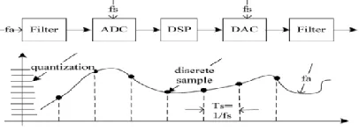
Analog-to-digital converters (ADCs) are key design blocks in modern microelectronic digital communication systems since they act as bridges between the analog and digital worlds. It is a necessary component whenever data from the analog domain, through sensors or transducers, should be digitally processed. Figure 1 depicts a typical signal processing system [1]. The analog input signal is first filtered to remove high-frequency components in order to avoid aliasing. Then the signal is sampled at frequency fS, and the discrete sampled data is quantized in the analog-to-digital converter (ADC). The digital outputs from ADC are executed in the digital signal processor (DSP). Finally, they return to an analog signal by the conversion of digital-to-analog converter (DAC) and smoothing of the followed reconstruction filter.
Figure 1 Basic signal processing system.
been able to benefit from process scaling in the same way as digital logic and therefore the relatively area-cheap digital logic is used to compensate for the shortcomings of expensive analog circuits.
Applications with Different Types of ADC Architectures
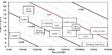
The four popular high-speed ADC architectures were described in the above sections. ADCs are selected according to specific application within the consideration of resolution, power, size, sampling frequency, performance and etc. Among the aforesaid four types of high-speed ADC, the time-interleaved ADC is a combination of several single channeled ADC, which is not suitable to be compared with the other three types of high-speed ADC architecture. So we just take the other three types of architectures, Flash, Pipeline and SAR as a comparison. For some applications, almost all the architectures may work well; for others, there may be a better choice to achieve the best performance. For example, a Flash ADC is most popular for applications requiring ultra-high speed when resolution and power consumption is not a primary concern; A SAR ADC is usually first considered to be implemented in the application of low power and small size with medium resolution[12-13]. Figure 2 shows the A/D converter application space according to different requirements of ADC sampling rate and resolution.
Figure 2 A/D Converter Application Space.
II. DESIGN CONSIDERATIONS
Static errors are deviation of converter transfer characteristics from ideal one. The static performance of an ADC is defined by these metrics: offset error, gain error, and nonlinearities like DNL error and INL errors.
DNL[k] – The difference between the code bin width of code k and the average code bin width, divided by the average code bin width after correcting for gain and offset.
DNL – The maximum absolute value of DNL for all
small INL. On the other hand, Figure 3 (b) suffers from large INL but relatively smaller DNL.
INL[k] – The difference between the ideal and actual code transition level k after correcting for gain and offset.
INL – The maximum absolute value of INL for all k.
As given in Figure 3 (a), these variations can be random with almost no correlation between successive steps. In this case the interpolating curve can be still very close the ideal one but the quantization error can vary significantly. In Figure 3 (b), the step size is small at the beginning but increases as the analog input becomes larger. Thus, there is a strong correlation between the successive steps and the interpolating curve moves away from the ideal one. However, the variation in the quantization error might be smaller [2]. To cover both of the cases presented in Figure 3, two different non-linearity specifications are used: 1) Differential Non-Linearity (DNL) and 2) Integral Non- Linearity (INL).
Figure .3 Two non-ideal transfer curves
Design considerations for SAR ADC with Binary-Weighted Capacitive DAC
P a g e | 411
Fig4 Conventional binary-weighted CDAC based SAR ADC (9-bit).
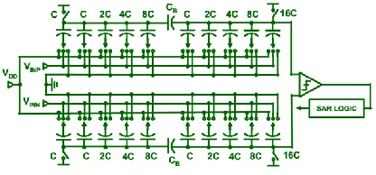
Split CDAC is one of alternative to reduce both input capacitance and area, shown in Figure 5, a fractional value bridge capacitor is implemented so that the two capacitor arrays have the same scaling [5]. In the charge redistribution, the total weight of the left array is equal to the weight of the lowest bit in the right array.
Figure 5 Differential split CDAC based SAR ADC (9-bit) (existing method)
The performance of this type of SAR ADC is limited by:
A. The comparator, which must resolve small differences in VIN and VDAC within the specified time with accuracy.
B. Each of the capacitors associated with the data bits would be exactly twice the value of the next-smaller capacitor, and the settling time of the DAC, which must settle to within the resolution of the overall converter, for example, ½ LSB.
Therefore, the two critical components of this type of SAR ADC are the comparator and the DAC. The requirements of the comparator are speed and accuracy. Although comparator offset does not affect overall linearity as it appears as an offset in the overall transfer characteristic, the comparator needs to resolve voltages within the accuracy of the overall system. Therefore, offset-cancellation techniques are usually applied to reduce the comparator offset. It needs to be as accurate as the overall system. The comparator is usually designed to have input-referred noise less than 1 LSB.
III.PROPOSED METHOD
The -based switching method proposed in halves the array capacitance leading to around 90% energy saving when compared with the conventional one. The details the Vcm-based switching algorithm. In the global sampling phase _1, Vin is stored in the capacitor array. During the conversion phase _2, all the capacitors’ bottom-plates are switched to the Vcm first, to give rise to the voltage −Vin at the output. The sign of Vout determines the MSB as the logic properly controls Sm,k−1. If −Vin < 0, Sm,k−1 goes to Gnd while the other switches Sm,k−2, …, Sl,0 remain connected to Vcm. If −Vin > 0, Sm,k−1 is switched to VDD. The cycle will be repeated for n − 2 times. The Vcm-based approach performs the MSB transition by connecting the differential arrays to Vcm.
The power dissipation is just derived from what is needed to drive the bottom-plate parasitic of the capacitive arrays, while in the conventional charge-redistribution where the necessary MSB “up” transition costs significant switching energy and settling time. Moreover, as the MSB capacitor is not required anymore, it can be removed from the n-bit DAC array. Therefore, the next n − 1 b estimation is done with an (n − 1) bit array instead of its n-bit counterpart, leading to half capacitance reduction with respect to the conventional method. Using supplies as reference voltages prevents static power dissipation from reference buffers.
Figure 6: Single-ended n-bit and (n − 1)-bit split capacitive DAC arrays (proposed method)
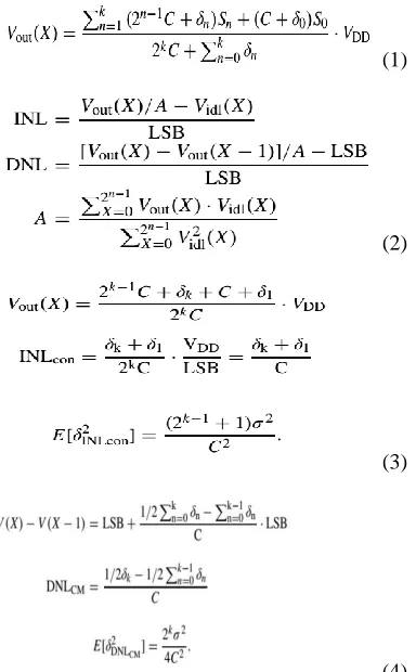
To calculate a given digital input X with its corresponding DAC output Vout (X),
(1)
(2)
(3)
(4)
So that the proposed method can achieve a DNL that is two times better in comparison to conventional switching. It can also be found that the error terms are decreased by half, which can be attributed to the cancellation of the terms. The capacitors contributing to two-bit transitions are correlated, which are switched from Vcm to VDD. In contrast, in the conventional method the capacitors connected to VDD in two-bit transitions are completely different, and the error terms are summed together instead of being cancelled.
VI.RESULTS ANALYSIS
(A)EXISTING SYSTEM-SPLIT SAR ADC
Figure 7: Analog input, digital output.INL &DNL errors for conventional SAR ADC
(B)PROPOSED SYSTEM - Vcm BASED SWITCHING METHOD
Figure 8: Analog input, digital output.INL &DNL errors for proposed Split SAR ADC
(C)Performance evolution:
Existing system:
Average value: 4.9648E-02
From 1.0000E-09 to 1.0000E-06 Maximum value: 1.0000E-02 at 9.5102E-07 From 1.0000E-09 to 1.0000E-06 Minimum value: 1.0000E-02 at 1.0000E-09 From 1.0000E-09 to 1.0000E-06 Peak to Peak value 9.0000E-02
From 1.0000E-09 to 1.0000E-06
Proposed system:
Average value: 4.9646E-03
From 1.0000E-09 to 1.0000E-06 Maximum value: 1.0000E-02 at 9.5102E-07
From 1.0000E-09 to 1.0000E-06 Minimum value: 1.0000E-03 at 1.0000E-09
From 1.0000E-09 to 1.0000E-06 Peak to peak value 9.0000E-03
From 1.0000E-09 to 1.0000E-06
V.CONCLUSION
P a g e | 413
and lower power is achieved by using Vcm-based switching.
REFERENCES
[1] J. Craninckx and G. V. Plas, “A 65 fJ/conversion-step 0-to-50 MS/s 0-to-0.7 mW 9b charge-sharing SAR ADC in 90 nm digital CMOS,” in IEEE Int. Solid-State Circuits Conf., Dig. Tech. Papers, Feb. 2007, pp. 246–247.
[2] V. Giannini, P. Nuzzo, V. Chironi, A. Baschirotto, G. Vander Plas, and J. Craninckx, “An 820 μW 9b 40 MS/s noise-tolerant dynamic-SAR ADC in 90 nm digital CMOS,” in IEEE Int. Solid-State Circuits Conf., Dig. Tech. Papers, Feb. 2008, pp. 238–610. [3] C. C. Liu, S.-J. Chang, G.-Y. Huang, and Y.-Z. Lin, “A 0.92 mW 10-bit 50-MS/s SAR ADC in 0.13 μm CMOS process,” in Symp. VLSI Circuits Dig. Tech. Papers, Jun. 2009, pp. 236–237. [4] P. Harpe, Z. Cui, W. Xiaoyan, G. Dolmans, and H. de Groot, “A 30 fJ/conversion-step 8b 0-to-10 MS/s asynchronous SAR ADC in 90 nm CMOS,” in IEEE Int. Solid-State Circuits Conf., Dig. Tech. Papers, Feb. 2010, pp. 388–389.
[5] M. Boulemnakher, E. Andre, J. Roux, and F. Paillardet, “A 1.2V 4.5 mW 10b 100 MS/s pipeline ADC,” in IEEE Int. Solid-State Circuits Conf., Dig. Tech. Papers, Feb. 2008, pp. 250–251. [6] S. T. Ryu, B. S. Song, and K. Bacrania, “A 10b 50 MS/s opamp-sharing pipeline A/D with current-reuse OTAs,” IEEE J. Solid-State Circuits, vol. 42, no. 3, pp. 475–485, Mar. 2007. [7] K. Chandrashekar and B. Bakkaloglu, “A 1.8-V 22-mW 10-bit 30MS/s pipelined CMOS ADC for low-power subsampling applications,” IEEE Trans. Very Large Scale Integr. (VLSI) Syst., vol. 19, no. 2, pp. 1610–1616, Sep. 2011.
[8] I. Ahmed, J. Mulder, and D. A. Johns, “A 50 MS/s 9.9 mW pipeline ADC with 58dB SNDR in 0.18 μm CMOS using capacitive charge-pumps,” in IEEE Int. Solid-State Circuits Conf., Dig. Tech. Papers, Feb. 2009, pp. 164–165.
[9] J. Hu, N. Dolev, and B. Murmann, “A 9.4-bit, 50-MS/s, 1.44-mW pipelined ADC using dynamic residue amplification,” in Symp. VLSI Circuits Dig. Tech. Papers, Jun. 2008, pp. 216–217. [10] O. A. Adeniran, A. Demosthenous, C. Clifton, S. Atungsiri, and R. Soin, “A CMOS low-power ADC for DVB-T and DVB-H systems,” in Proc. IEEE Int. Symp. Circuits Syst., vol. 1. May 2004, pp. 209–212.
[11] U.-F. Chio, H.-G. Wei, Z. Yan, S. Sai-Weng, U. Seng-Pan, R. P. Martins, and F. Maloberti, “Design and experimental verification of a power effective Flash-SAR subranging ADC,” IEEE Trans. Circuits Syst. II, Exp. Briefs, vol. 57, no. 8, pp. 607– 611, Aug. 2010.
[12] Y. Zhu, U.-F. Chio, H.-G. Wei, S.-W. Sin, U. Seng-Pan, and R. P. Martins, “A power-efficient capacitor structure for high-speed charge recycling SAR ADCs,” in Proc. IEEE Int. Conf. Electron. Circuits Syst., Aug.–Sep. 2008, pp. 642–645.
[13] Z. Cao, S. Yan, and Y. Li, “A 32 mW 1.25 GS/s 6b 2b/step SAR ADC in 0.13 μm CMOS,” in Int. Solid-State Circuits Conf. Dig. Tech. Papers, pp. 542–543, Feb. 2008.
[14] M. Saberi, R. Lotfi, K. Mafinezhad, and W. A. Serdijn, “Analysis of power consumption and linearity in capacitive digital-to-analog converters used in successive approximation ADCs,” IEEE Trans. Circuit Syst. I, Regular Papers, vol. 58, no. 8, pp. 1736–1748, Aug. 2011.
[15] Y.-K. Cho, Y.-D. Jeon, J.-W. Nam, and J.-K. Kwon, “A 9-bit 80 MS/s successive approximation register analog-to-digital converter with a capacitor reduction technique,” IEEE Trans. Circuit Syst. II, Exp. Briefs, vol. 57, no. 7, pp. 502–506, Jul. 2010.
Parasa Anitha
14ND1D5709 Student M.Tech Student Scholar
Father Name:Sambasivarao Department of Electronics & Communication Engineering, Specialization: VLSI
St.Mary’s Women’s Engineering College, Budampadu, Guntur district, A.P, India.
[email protected] +91 9652068151
A.Radha,
Asst.professor,Department of Electronics & Communication,Engineering,St.Mary’s omen’s Engineering College, Budampadu, Guntur district, A.P, India.