REDDY, PRAMOD. A Study of Surfaces, Interfaces and Point Defect Control in III-Nitrides. (Under the direction of Zlatko Sitar and Ramon Collazo).
The origin of the bandgap bowing is found to be in the conduction band. Passivation studies include LPCVD and PECVD silicon nitride and PECVD silicon dioxide deposited on AlxGa1-xN (of varying Al composition ‘x’). Among these LPCVD silicon nitride is found to be most promising and forms a type II staggered band alignment with AlGaN for all Al compositions (0≤x≤1) and presents an electron barrier into AlGaN even at higher Al compositions where Eg(AlGaN)>Eg(Si3N4). Further, strong indications (via I-V-T, C-V-T and XPS studies) of greatly reduced interface states and hence excellent passivation for all Al compositions is observed.
by Pramod Reddy
A dissertation submitted to the Graduate Faculty of North Carolina State University
in partial fulfillment of the requirements for the degree of
Doctor of Philosophy
Materials Science and Engineering
Raleigh, North Carolina 2016
APPROVED BY:
____________________________ ____________________________
Dr. Zlatko Sitar Dr. Ramon Collazo
Committee Co-chair Committee Co-chair
____________________________ ____________________________
BIOGRAPHY
ACKNOWLEDGMENTS
TABLE OF CONTENTS
LIST OF FIGURES ... ix
LIST OF TABLES ... xviii
1 CHAPTER 1: Introduction to Al/Ga-nitrides ... 1
Dissertation Overview ... 1
Crystal structure, bandgap and polarization density ... 3
Growth of Al/Ga-Nitrides ... 10
1.3.1 Substrates for nitride growth: sapphire ... 10
1.3.2 Substrates for nitride growth: single crystalline AlN ... 11
1.3.3 Epitaxial Growth of III-nitrides by Metal organic chemical vapor deposition (MOCVD) ... 15
Defects in Al/Ga-Nitrides ... 19
1.4.1 Point defects ... 19
1.4.2 Extended defects in III-Nitrides ... 24
Al/Ga-Nitride technology: Challenges and motivation ... 25
2 CHAPTER 2: A surface study of AlN and GaN... 30
2.1 Introduction. ... 30
2.2 Growth, surface preparation and experimental setup ... 31
2.4 Charge neutrality levels, Fermi level pinning and barrier heights ... 34
2.5 Polarization charge compensating surface states and electron affinity ... 44
2.6 Conclusions ... 46
3 CHAPTER 3: a surface study of the alloy AlGaN ... 47
Introduction ... 47
Growth, sample pretreatment and experimental setup ... 48
Surface chemical composition ... 48
Charge neutrality levels and barrier heights ... 49
Surface work function and electron affinity of AlGaN ... 52
Band offsets in ALGaN ... 55
Conclusion ... 56
4 CHAPTER 4: Schottky contacts on AlN and Al rich AlGaN ... 58
Introduction ... 58
Growth, sample pretreatment and experimental setup ... 60
Schottky contacts on polar and non-polar AlN ... 61
Schottky contacts on AlGaN ... 68
Conclusion ... 69
5 CHAPTER 5: Schottky contacts on GaN ... 72
Introduction ... 72
Ni-Schottky diode on GaN: Electrical properties and thermal stability ... 73
Conclusion ... 80
6 CHAPTER 6: Passivation of Al/GaN – a dielectric/AlGaN interface study ... 81
Introduction ... 81
Growth, surface preparation and experimental setup ... 83
Stoichiometry, chemical composition and surface morphology of dielectric films 84 Dielectric-AlGaN band offsets ... 87
6.4.1 LPCVD silicon nitride ... 87
6.4.2 PECVD silicon nitride ... 90
6.4.3 PECVD Silicon dioxide ... 90
Analysis of dielectric-AlGaN interface states and passivation ... 92
6.5.1 LPCVD stoichiometric silicon nitride ... 92
6.5.2 PECVD silicon nitride and silicon dioxide ... 100
CONCLUSIONS ... 101
7 CHAPTER 7: Point defect reduction in Al/GaN – theory and implementation of chemical potential control ... 103
Introduction ... 103
Relationship between growth conditions and chemical potentials of III and N
Point defect reduction of CN in GaN by chemical potential control ... 107
Conclusion ... 117
8 CHAPTER 8: Point defect reduction in Al/GaN – theory and implementation of defect quasi Fermi level control ... 118
Introduction ... 118
Theory ... 120
8.2.1 Relationship between energy of formation and defect quasi Fermi level (DQFL) 120 8.2.2 The relationship between defect quasi fermi level and defect energy and photo-voltage ... 126
8.2.3 Efficiency: Work done against defect formation ... 130
8.2.4 DQFL and Fermi level: Modified formation energy diagrams ... 133
8.2.5 Rules of point defect control ... 135
Case study with DQFL based point defect reduction in GaN ... 139
Evidence for role of minority carriers ... 146
Conclusion ... 150
9 CONCLUSIONS AND OUTLOOK ... 152
Conclusions ... 152
Outlook ... 157
LIST OF FIGURES
Figure 1-1: Unit cell of GaN with [1 0 0] perpendicular to plane of paper. ... 4 Figure 1-2: An illustration of the (a) surface polarization charge and (b) interface polarization charge in AlGaN. ... 8 Figure 1-3: An illustration of the piezoelectric polarization in AlGaN heterojunctions. 9 Figure 1-4: The crystal structure of sapphire with [100] perpendicular to plane of paper. ... 11 Figure 1-5: The (0 0 0 1) planes of (a) III-N and (b) sapphire. The highlighted unit cell of III-N is lattice matched to highlighted Al sub-lattice resulting in a rotation of 30o with the larger highlighted unit cell of sapphire. ... 13 Figure 1-6: The (a) temperature dependence of standard free energy of AlN and (b) the decomposition temperature as a function of partial pressure of nitrogen. The standard free energies are obtained from NIST-JANAF Thermochemical Tables, 4th Edition37 ... 14 Figure 1-7: (a) PVT grown single crystalline AlN boule and (b) polished AlN wafer obtained from the boule. (c) AFM analysis of the surface cleaned substrate
Figure 1-11: The formation energy of CN as a function of Fermi level in GaN.60 ... 22 Figure 1-12: A comparison of the specific on-resistance for a design breakdown voltage for SiC, GaN and AlN. ... 27 Figure 1-13: The bandgap of AlGaN and the corresponding emission wavelength as a function of Al molar fraction. Some applications75–78 in each of the UV-regions: A,B and C are also provided. ... 29 Figure 2-1: Molar fractions of Ga, N, and O on Ga- and N-polar surfaces. ... 33 Figure 2-2: XPS valence band data fitted to Gaussian broadened theoretical VDOS of (a) n-type, Ga-polar GaN and (b) m-plane AlN. ... 36 Figure 2-3: Surface state initiated band bending at the surface in Ga-polar, n-type (a) and p-type (b) GaN. ... 38 Figure 2-4: Increased CNL on a) c-plane due to positively charged surface states in comparison with b) non-polar m-plane AlN. ... 39 Figure 2-5: (a) Decrease in electron affinity on N-polar GaN due to surface dipole and (b) increase in electron affinity on Ga-polar GaN due to surface dipole ... 45 Figure 3-1: Measurement of the CNL using XPS valence band data of (a) Si doped Al0.85Ga0.15N and (b) Mg doped Al0.7Ga0.3N grown on AlN via comparison with theoretical VDOS. The dashed and solid lines represent the calculated and
Mg doped (75%) AlGaN is grown on AlN. The rest are Si doped. Dashed lines are interpolations between AlN and GaN. ... 52 Figure 3-3: Binding energies of Al 2p and Ga 3d core levels as a function of AlGaN composition in films that were grown on AlN single crystalline substrate and
sapphire. 25% and 40% AlGaN are unintentionally doped. Mg doped (75%) AlGaN is grown on AlN. The rest are Si doped. ... 53 Figure 3-4: The band divergence in AlGaN as a function of composition determined using CNL, barrier height at CNL and the constant work function of 3.7 eV. (Dashed lines represent the interpolations) ... 56 Figure 3-5: Conduction band offset (ΔEc), as a function of Al composition of the two layers forming the heterojunction. The dependence of the ratio of conduction band offset and valence band offset on Al composition is also shown. ... 57 Figure 4-1: The core level peaks (a) Al 2p and (b) N 1s referenced with respect to the VBM ... 62 Figure 4-2: Measured molar fractions of various metals as a function of film
Figure 4-5: A comparison of measured barrier heights on c-plane and m-plane AlN plotted as a function of electronegativity differences between AlN and various
metals. ... 70 Figure 4-6: The experimental Ni Schottky barrier heights on AlGaN at different compositions in comparison with the proposed barrier height model. Other
experimental results from Reddy et al.120, Xie et al.2 and Tweedie et al.99 ... 71 Figure 5-1: I-V characterization of Ni Schottky diodes on n-GaN without surface treatment exhibiting high ideality factor and a “shoulder” at low voltages which is found to be a large parallel resistance from log(I)-log(V) plots. ... 74 Figure 5-2: (a) I-V characteristics of annealed contacts metallized without surface treatment showing improved ideality factor and barrier height. Note the absence of additional leakage at low voltage. (b) Reverse leakage characteristics of Ni/n-GaN Schottky diodes processed by photolithography annealed at various temperatures. ... 75 Figure 5-3: (a) XPS core level analysis of C 1s showing C compounds on developed surface partly comprising of C-N bonds and (b) XPS quantitative chemical analysis showing surface chemical composition of GaN at various stages of contact
processing. C(ref) typically corresponds to “adventitious C” in XPS analysis. O is <5% at all stages. ... 76 Figure 5-4: (a)I-V-T and (b)C-V-T characterization of Ni contacts with post
Figure 5-6: Reverse leakage characteristics of Ni/n-GaN Schottky diodes processed with different surface treatments before photolithography relative to clean contact deposition via shadow mask. ... 79 Figure 6-1: (a) Silicon core level (Si 2p) peaks at 101.9 and 103 eV corresponding to the Si nitride and oxide bonds, respectively. AFM characterization (b and c) showing uniform conformal deposition of silicon nitride on GaN. ... 85 Figure 6-2: (a) Silicon core level (Si 2p) peaks at 99.3, 100.9 and 102.9 eV
corresponding to the amorphous Si/Si-H, Si (rich)-N and Si-O bonds, respectively. (b) AFM characterization showing. (c) Silicon core level (Si 2p) peaks at 102.9 eV corresponding only to Si-O bonds. ... 86 Figure 6-3: XPS valence band data from the surface of thick silicon nitride film showing the valence band maximum at 3 eV with respect to the surface Fermi level. ... 89 Figure 6-4: The (a) electronic band alignment and (b) band offsets at silicon
nitride/AlGaN interface with different Al compositions. ... 89 Figure 6-5: XPS valence band data from the surface of thick PECVD (a) silicon nitride and (b) silicon dioxide showing the valence band maxima with binding
Figure 6-8: The band bending at the interface of silicon nitride and AlGaN in
comparison with that at the free surface as a function of Al molar fraction. ... 94 Figure 6-9: I-V characteristics of silicon nitride/n-GaN heterostructure. ... 97 Figure 6-10: C-V characterization of (a) silicon nitride/n-GaN and (b) silicon nitride/p-GaN heterostructures. ... 98 Figure 6-11: C-V characterization of silicon nitride (2 nm)/n-Al0.6Ga0.4N
Figure 7-3: The change in chemical potentials of nitrogen, alkanes and hydrogen as a function of V/III ratio under (a) hydrogen and nitrogen diluents and low V/III ratios (NH3 flow as variable) and (b) hydrogen diluent at high V/III ratios (TEG flow as variable). T=1050 oC ... 111 Figure 7-4: The (a) theoretical fit predicting the change in incorporation of CN in comparison with experimental data as a function of V/III ratios and diluent gas and (b) corresponding shift in formation energy with respect to reference growth state. ... 115 Figure 7-5: The change in formation energy of CN and hence its incorporation in comparison with experimental data at different temperatures. Note that the reference growth state is chosen to be V/III=2000, T=1050 oC (1323 K), H2 diluent and P=20 Torr. ... 116 Figure 8-1: (a) The dependence of dQFL on (a) the defect energy at different
Figure 8-13: An illustration of decrease in CN density relative to equilibrium
LIST OF TABLES
Table 1-1: Lattice and polarization parameters of AlN and GaN1,5–7 ... 3 Table 1-2: The piezoelectric and elastic tensor elements for AlN and GaN that
determine the piezoelectric density7,8 ... 9 Table 1-3: A comparison of GaN, AlN, SiC and Si illustrating their relative
performance in power-electronic applications79–82. ... 26 Table 2-1: The measured positions of the Fermi level at the surface (CNL), carrier concentration (n), calculated bulk Fermi level (Ef) at 300K, and barrier heights (φb) in GaN ... 37 Table 2-2: The measured positions of the Fermi level at the surface (CNL) and barrier heights (φb) in AlN epitaxial films and substrates ... 40 Table 2-3: Experimental and theoretical values for density of surface states (Ds), branch point energies, spontaneous polarization charge (σsp) and barrier shift (Δφ) in AlN and GaN. ... 42 Table 4-1: The models describing the behavior of the Schottky barrier and the
1 CHAPTER 1: Introduction to Al/Ga-nitrides
Dissertation OverviewAlN, GaN and their alloy AlGaN are of high interest in power electronics due to their excellent dielectric strength, temperature stability and carrier mobility thus making them ideal for fabricating high power and high frequency switches.1–3 Further the large tunable direct bandgap of AlGaN along with the high internal quantum efficiencies makes it an ideal choice in deep UV optoelectronics including laser diodes.4 However, there are two extant classes of challenges in implementing nitride based power electronics and optoelectronics: compensating point defects and mid-gap surface states. In this thesis, a study on control and reduction of surface and bulk defects is presented to help in predicting, designing, implementing and improving the performance of III-Nitride based devices.
Chapter 1 presents an introduction to the material system and relevant properties. Bulk and epitaxial crystal growths, crystal defects and their causal role in current technological limitations are also described here.
relatively low, metal independent, Schottky barrier height (<1 eV) is demonstrated in GaN, a significant obstacle in implementing high breakdown voltage vertical Schottky devices. Although the barrier heights are found to be higher in AlGaN, the presence of mid-gap states are confirmed which form an obstacle in high frequency switching and performance drift. The surface passivation of AlGaN is hence found to be necessary for high frequency operation and higher barriers and a passivation scheme via high temperature low pressure chemical vapor deposition silicon nitride is presented in chapter 6.
Crystal structure, bandgap and polarization density
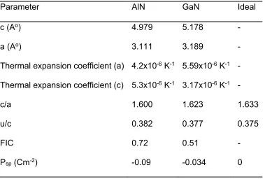
Thermodynamically stable crystal structure of Al/Ga-nitrides is the wurtzite structure with zinc blende being stabilized only on {011} cubic substrates.1 The wurtzite structure consists of two hexagonal close packed sub-lattices of III and N atoms arranged as A(III)A(N)B(III)B(N)A(III)A(N)… stacks with two formula units per unit cell shown in Figure 1-1. The Ga atoms are at [0 0 0 0] and [1/3 2/3 -1 1/2] and N atoms are at [0 0 0 u] and [1/3 2/3 -1 ½+u] where u is the Ga-N bond length. For an ideal wurtzite structure, c/a=√8/3=1.633, u=3/8*c=0.375c and the N-Ga-N bond angle=109.45 o. It Is clear that the configuration number for III(N) atoms is 4 with III(N) at the center and N(III) at the vertices of a regular tetrahedron.1 The lattice parameters of GaN and AlN are tabulated in Table 1-1.
Table 1-1: Lattice and polarization parameters of AlN and GaN1,5–7
Parameter AlN GaN Ideal
c (Ao) 4.979 5.178 -
a (Ao) 3.111 3.189 -
Thermal expansion coefficient (a) 4.2x10⁻⁶ K-1 5.59x10⁻⁶ K-1 - Thermal expansion coefficient (c) 5.3x10⁻⁶ K-1 3.17x10⁻⁶ K-1 -
c/a 1.600 1.623 1.633
u/c 0.382 0.377 0.375
FIC 0.72 0.51 -
Figure 1-1: Unit cell of GaN with [1 0 0] perpendicular to plane of paper.
The ternary alloy AlGaN exhibits a lattice constant that follows Vegard’s law i.e. a linear interpolation between lattice constants of GaN and AlN and is given by,8
1
3.189 0.078x AlN GaN
a xa x a x Ao (1.1)
and
1
5.178 0.199x AlN GaN
c xc x c x Ao. (1.2)
GaN and AlN are wide direct bandgap semiconductors whose temperature dependent bandgaps are given by,9
2 4
(0) 9.39 10
772
g g
T
E E eV
T
and (0) 1.799 103 2
1462
g g
T
E E eV
T
where Eg(0)=6.1 eV (1.4)
respectively. Although the lattice constants follow Vegard’s law, the bond lengths exhibit a non-linear dependence on composition.10 Hence the alloy AlGaN has a bandgap expressed by Vegard’s law with an empirical quadratic correction implemented by a bowing parameter b. The bandgap of AlxGa1-xN is hence
( ) AlN 1 GaN 1
g g g
E x xE x E bx x . (1.5)
Expectedly, the bowing parameter is also dependent on strain and there is large variability in the reported bowing parameters (-0.8 eV to 2.6 eV) possibly due to varying crystal quality.11 A bowing parameter is expected to be 0.7 to 1 eV in high quality films.10,11
The ionic nature of the III-N bond results in a dipole moment rdirected towards the III atom, where δ is the partial positive(negative) charge on III(N) atoms and r is the bond length. The partial charge is a function of fractional ionic character (FIC) defined
as III N
III N Q Q FIC Q Q
where Q is the effective charge on III/N atoms. A fully covalent
bond has QIII=QN=4 with FIC=0 and a fully ionic bond as QIII=0 and QN=8 with FIC=1. The Ga-N and Al-N bonds have partial ionic character with FICGaN= 0.51 and FICAlN=0.72.12 The Polarization Density P (Cm-2) is defined as dipole moment per unit volume and is given by
where n is the dipole density. The electric field associated with the polarization density is then
P E
(1.7)
where ε is the dielectric constant. Hence a net dipole per unit cell results in finite P defined as spontaneous polarization charge and an associated electric field. Consider an ideal tetrahedron with Ga atom at the center and N at the vertices shown in Figure 1-1. The vector sum of dipole moments associated with the four Ga-N bonds is zero. Hence, in an ideal wurtzite structure with ideal tetrahedra, the net dipole moment, and hence spontaneous polarization is zero. However, the wurtzite structure is distorted in III-nitrides. The distortion is such that c/a<1.633, u/c>0.375 and N-(Ga-N along c-axis) bond angle<109.45o with a resulting net dipole moment in [0 0 0 -1] (-c) direction. The experimentally determined deviations of lattice parameters from ideal wurtzite structure reported for GaN and AlN and the corresponding spontaneous polarization density are shown in Table 1-1.
Similar to lattice parameters, the spontaneous polarization in AlxGa1-xN is assumed to follow Vegard’s law10 i.e. a linear interpolation between AlN and GaN given by
Al
1
Ga 0.055 0.032 2sp sp sp
P x xP x P x Cm . (1.8)
volume. Since P is independent of lattice translation in the bulk of the semiconductor, 0
P P
. However, a discontinuity in dipole moment per unit cell occurs at the
surface and a heterojunction. Consequently, a surface/interface charge density may be defined as
2ˆ ˆ ˆ 0.055 0.032
surface
P s PAlGaN s c x Cm
(1.9)
and
1 1
/ ˆ ˆ ˆ 0.055 2
x x y y
x y
P s PAl Ga N PAl Ga N s c x y Cm
(1.10)
properties (described in chapter 2) and passivation techniques (chapter 6) is presented.
Figure 1-2: An illustration of the (a) surface polarization charge and (b) interface polarization
charge in AlGaN.
Deviations from an ideal wurtzite structure due to strain also generates a net dipole moment per unit cell volume defined as piezoelectric polarization density P e , where e and ε are piezoelectric and strain tensors. For hexagonal symmetry,
15 24 31 33 2 x xz y yz
z xx zz
P e
P e
P e e
(1.11)
For III-Nitrides, the piezoelectric polarization density Pz along c-axis is the only non-zero component with Px=Py=0. For growth along c-direction, a biaxial strain in (0 0 0
1) given by 0
0
xx yy
a a a
, where a and a0 are the strained and relaxed lattice
depends on the Poisson’s ratio
1333zz
xx yy
c c
, where c13 and c33 are elastic tensor
elements. From equation (1.11), the piezoelectric polarization density is given by
0 13
31 33
0 33
2
PP
a a c
P e e
a c
. (1.12)
Figure 1-3: An illustration of the piezoelectric polarization in AlGaN heterojunctions.
Table 1-2: The piezoelectric and elastic tensor elements for AlN and GaN that determine the
piezoelectric density7,8
Parameter AlN GaN e31 (Cm-2) -0.53 -0.34 e33 (Cm-2) 1.5 0.67 c13 (GPa) 94 68 c33 (GPa) 377 354
lattice constants and spontaneous polarization, the piezoelectric polarization tensor elements are assumed to follow Vegard’s law in AlGaN.10,14 Typically, for AlGaN heterojunctions, Psp>Ppp and spontaneous polarization typically determines the sign of the polarization charge, in contrast to InGaN/GaN heterojunctions, where piezoelectric polarization dominates. Additional details may be found elsewhere.10
Growth of Al/Ga-Nitrides
1.3.1 Substrates for nitride growth: sapphire
lowered luminescence efficiencies21 and carrier mobilities22 and consequently device performance. The thermal conductivity of sapphire (~0.25 to 0.5 Wcm-1K-1 at 300K23) is also relatively poor resulting in poor thermal dissipation in high power electronics applications.23
Figure 1-4: The crystal structure of sapphire with [100] perpendicular to plane of paper.
1.3.2 Substrates for nitride growth: single crystalline AlN
work, homo-epitaxy utilizes single crystalline AlN as substrates for growth of AlN and AlGaN. Single crystals of AlN are grown by physical vapor transport (PVT). Consider the dissociation reaction
2 1 ( ) ( )
2
AlN s Al N g . (1.13)
elsewhere.28–34 The resulting boules were sliced into wafers shown in Figure 1-7(b) by diamond wire saw in the desired orientations and mechanically and chemo-mechanically polished into epi-ready substrates (Figure 1-7(c)).39 These substrates have dislocation densities < 103 cm-2.39
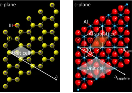
Figure 1-5: The (0 0 0 1) planes of (a) III-N and (b) sapphire. The highlighted unit cell of III-N
is lattice matched to highlighted Al sub-lattice resulting in a rotation of 30o with the larger
highlighted unit cell of sapphire.
then rinsed in DI water and dried under N2. Further details on substrate preparation are found elsewhere.35,36
Figure 1-6: The (a) temperature dependence of standard free energy of AlN and (b) the
decomposition temperature as a function of partial pressure of nitrogen. The standard free
energies are obtained from NIST-JANAF Thermochemical Tables, 4th Edition37
Figure 1-7: (a) PVT grown single crystalline AlN boule and (b) polished AlN wafer obtained
from the boule. (c) AFM analysis of the surface cleaned substrate exhibiting atomic (bi-layer)
1.3.3 Epitaxial Growth of III-nitrides by Metal organic chemical vapor
deposition (MOCVD)
Metal organic chemical vapor deposition (MOCVD) utilizes metal-organic precursors of III-atoms which decompose at growth temperatures to provide Ga/Al vapor. In this work, triethylgallium and trimethylaluminum are the metal-organic precursors employed. Further a reactive source of nitrogen, ammonia is the N precursor. Growth occurs by the following reaction at nitride surface:
3 2
3 2
g
III NH IIIN H (1.14)
For sufficient reaction and growth rates, the growth temperatures>1000 oC (1273 K) are required. The standard free energy of formation of GaN is shown in Figure 1-8(a) indicating decomposition at 1100K at 1 atm of N2. Correspondingly, the equilibrium temperature for GaN dissociation into Ga(liquid) and N2 as a function of reactor partial pressure of N2 is shown in Figure 1-8(b).
It is clear that, to prevent decomposition of GaN at growth temperatures, high partial pressures of N2 (>100 atm) is necessary. However, it is found that GaN surface is stabilized in NH3 atmosphere at much lower partial pressures. The equilibrium partial
pressures of NH3 and N2 are related by
32 2 1/2 3/2 NH N N H P P K P
, where KN~3000.38
ammonia flow to metal organic flow (V/III ratio) being much larger than 1 (typically >100).
Figure 1-8: The (a) temperature dependence of standard free energy of GaN and (b) the
decomposition temperature as a function of partial pressure of nitrogen. The standard free
energies are obtained from Jacob and Rajitha.39
Epitaxial growth on stabilized GaN surface occurs by the chemical reaction (1.14) where the equilibrium constant is given by
2 33/2
eq
MN H
eq eq III NH
a P
K
P P
(1.15)
where ‘P’ is the partial pressure and ‘a’ is the activity of the nitride. The equilibrium constants are reported to be40
1.78 104
log K 12.2 1.79log T
T
for GaN (1.16)
3.17 104
log K 14.2 2.33log T
T
for AlN. (1.17)
Typical growth temperatures are 1000oC<T<1100oC. If in III
P and
3
in NH
P are the input
partial pressures of Al/Ga and NH3 respectively, the driving force for the reaction (1.14) is
2 2 2 3
3 3
2 3
3/2 3/2 3/2
3/2
ln ln ln
eq in in eq eq
MN H MN H H III NH
eq eq in in eq in in
III NH III NH H III NH
a P a P P P P
G RT RT RT
P P P P P P P
. (1.18)
The driving force may be expressed in terms of supersaturation defined as
in eq
eq
P P
P
or1 Peqin P
(1.19)
For growth, G 0and consequently σ>1 are required. From equation (1.15), it is clear that the equilibrium partial pressures are related via equilibrium constant by law of mass action. As described earlier, the reactor is ammonia rich
3, 3 ,
in eq in eq
NH NH III III
P P P P .
Consequently, conservation of molar mass for reaction (1.14) requiring
3 3
in eq in eq
III III NH NH
P P P P during growth, ensures in3 eq3
NH NH
P P and in2 eq2
H H
P P . Hence ammonia
and hydrogen supersaturations are close to zero. The driving force is primarily dependent on metal partial pressures only and is given by
sup ln ln 1
in III III eq III P
G RT RT
P
, (1.20)
in eq III III
III eq
III
P P
P
. (1.21)
Figure 1-9: A vertical, cold-wall, rf-heated MOCVD reactor
Defects in Al/Ga-Nitrides
Defects in III-nitride crystals determine the electronic and optical properties of the active regions in device structures and consequently determine the feasibility of III-nitride based optoelectronic and high power-electronic devices. In general, defects are classified into point and extended defects based on dimensionality.
1.4.1 Point defects
Point defects (zero-dimensional) may refer to intentionally introduced impurities such as dopants that are required to form functional hetero-junctions (e.g p-n junction) in electronic or optical devices or unintentionally introduced impurities or native defects such as vacancies that may be detrimental to device performance. The tendency to incorporate a particular defect during growth processes may be represented by the formation energy of the defect. For a defect with charge state q, in a material at equilibrium, it is defined as41
f q q
ref j j F V
j
E X E X
n q E E (1.22)growth of Al/GaN is a mass transport limited process and supersaturation-chemical potential drop is primarily across the boundary layer.43 Consequently, the growth surface is expected to be near equilibrium and the defect incorporation is theoretically described using chemical potentials and Fermi level at the surface in chapters 7 and 8.
1.4.1.1 Dopants in Al/Ga-nitrides
Al/GaN may be doped as n-type or p-type by introducing appropriate substitutional impurities during growth. The typically used n-type and p-type dopants are Si and Mg respectively and are employed in this work. Si with a valency of 4 and Mg with valency of 2 substitute Ga (valency of 3) to function as donor and acceptor respectively. Si is an excellent donor in AlGaN with activation energy comparable to thermal energy at room temperature for Al molar fractions <0.844,45 as shown in Figure 1-10(a). However, at higher Al compositions (x>0.8), Si self-compensates by DX center formation resulting in a sharp increase in activation energy.46 Further, at higher doping levels in Al rich AlGaN, increased compensation, possibly by native defects, reduces carrier concentration and mobility.24 Consequently, significant difficulties are seen in obtaining high carrier concentrations at higher Al compositions. Another important consequence of DX center formation is the lack of significantly conducting AlN substrates.
magnesium is passivated and p-type GaN is highly resistive in as-grown state. Post-growth thermal annealing is necessary to activate magnesium.47 The acceptor activation energy further increases with increase in Al composition as shown in Figure 1-10(b) thereby resulting in insulating films at room temperatures.45,48–53 Hence low resistivity p-type Al rich AlGaN is currently a significant challenge and devices requiring p-type AlGaN to produce required p-n junctions. Hence alternative techniques to inject holes including p-GaN injection layers, Mg-doped AlGaN super-lattices etc. are employed.54,55
Figure 1-10: The activation energies of (a) SiGa and (b)MgGa as a function of Al
composition.44,45,48–53
1.4.1.2 Compensating point defects
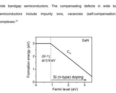
an acceptor with (0/-1) transition at 0.9 eV as shown in Figure 1-11 and is a major compensating defect in MOCVD grown AlGaN.60 From equation (1.22), the formation energy of CN decreases when Si doped and its incorporation correspondingly increases. In general, due to this dependence of compensating defect formation energy on the Fermi level, point defect control is found to be a more serious issue in wide bandgap semiconductors. The compensating defects in wide bandgap semiconductors include impurity ions, vacancies (self-compensation) and complexes.41
Figure 1-11: The formation energy of CN as a function of Fermi level in GaN.60
1.4.1.3 Point defect control
of growth conditions on incorporation of various defects exist, quantitative theoretical models describing the dependence of point defect incorporation on growth conditions or formulating the growth parameters in terms of chemical potentials have been limited. Density functional theory (DFT) analyses of point defects in III-nitrides including more accurate models in recent years have described their formation energies in terms of chemical potentials of III/Nitrogen and impurity atoms associated with the defect.41,46,62–64 In chapter 7, thermodynamic models of MOCVD growth reactions in Al/Ga nitrides and reported DFT analyses are related via difference equations of chemical potentials and a theoretical model that provides quantitative relationship between point defect formation energies (i.e. incorporation) and growth parameters including V/III ratio, partial pressures, diluent gases and temperature is proposed.
a technique is that its use does not alter the growth conditions. In this work, (chapter 8) a general theory of compensating defect density reduction via an increase of the formation energy of defects through the modification of defect quasi Fermi level (dQFL) achieved by introduction of excess minority carriers into the system is presented. The proposed theoretical model is shown to be successful in predicting the existence of a defect energy dependent process efficiency with excellent qualitative and quantitative agreements with experimental data. The proposed theory is also material independent and may be applied to the doping process of any semiconductor.
1.4.2 Extended defects in III-Nitrides
1].65,69 The screw type dislocations may develop to accommodate strain due to growth along stepped substrate surface.65 The elastic energy stored in edge and screw dislocations is given by
2
Ekb (1.23)
where k is the elastic modulus tensor and b is the Burgers vector. The ratio of energies stored in screw to edge dislocations is ~1.66 ensuring higher densities of edge dislocations.65 Various techniques have been employed to reduce threading dislocation density including epitaxial lateral overgrowth70 and AlN buffer layers71 and consequently improved electrical and optical properties of III-Nitride epitaxial films. However, for applications in deep UV lasers, the dislocation density required is <107 cm-2.67 AlGaN films on sapphire typically have dislocation densities ~1010 cm-2 and may be reduced to ~5x107 cm-2 by appropriate buffer layers, masks and templates.71 Consequently single crystalline AlN substrates for growth and fabrication of high Al composition AlGaN based deep-UV optoelectronics with dislocation densities <104 cm-2 may be the most feasible option to obtain deep-UV lasers and deep UV optoelectronics in general.
Al/Ga-Nitride technology: Challenges and motivation
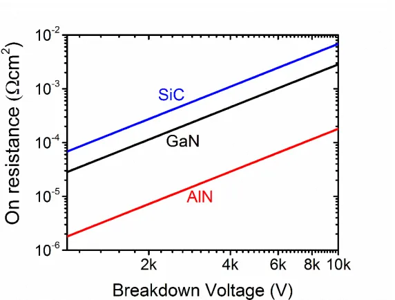
1-12 relative to SiC. The resulting Baliga’s figures of merit (BFOM) of GaN and AlN are expected to be better than silicon carbide with AlN being vastly superior as shown in Table 1-3. It is obvious that Al/GaN provides a vast improvement over existing technologies based on Si and SiC.
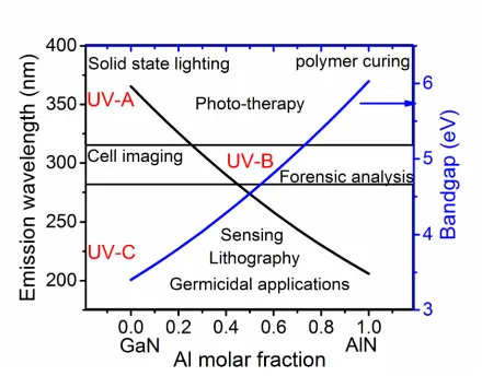
Further, the alloy system of AlGaN enables deep-UV optoelectronics with wavelengths ranging from 365 nm (UV-A) to 206 nm (UV-C) due to the tunable direct bandgap and high photoluminescence efficiencies.25 Consequently, AlGaN based optoelectronics finds great interest in applications ranging from solid state lighting, photo-therapy, polymer curing, cell imaging, forensic analysis, sensors, lithography, water purification, disinfection etc.79–82 The bandgap range of AlGaN and the corresponding range of emission wavelengths are shown in Figure 1-13 as a function of Al composition.
Table 1-3: A comparison of GaN, AlN, SiC and Si illustrating their relative performance in
power-electronic applications72–78.
Property AlN GaN 4H-SiC Si
Breakdown field (MVcm-1) 15 3.75 3 0.3 Electron mobility cm2/Vs(300K) 300 >1000 500-700 <1400
Bandgap (eV) (300K) 6.03 3.4 3.23 1.12
Figure 1-12: A comparison of the specific on-resistance for a design breakdown voltage for
SiC, GaN and AlN.
calculation) and difficulties in achieving conducting substrates required in vertical power devices.46 Further, as discussed earlier, compensating defect incorporation reduces carrier concentrations, carrier mobility and internal quantum efficiencies thereby limiting or precluding both high power Schottky diodes and deep-UV LEDs and Lasers. Consequently, it may be concluded that implementation of AlGaN technologies are currently limited by lack of good control over surface defects and bulk defects.
Figure 1-13: The bandgap of AlGaN and the corresponding emission wavelength as a function
of Al molar fraction. Some applications79–82 in each of the UV-regions: A,B and C are also
2 CHAPTER 2: A surface study of AlN and GaN
2.1 Introduction.states is unknown. Further, studies on surface states and Fermi level pinning on AlN surface is limited. Additionally, barrier heights reported on p-type GaN show the Fermi level pinned at a lower than expected energy at the surface, i.e., the sum of barrier heights on p-type and n-type GaN is much lower than the bandgap.92,93 In this chapter, x-ray photoelectron spectroscopy (XPS) is used to provide experimental proof for Fermi level pinning by donor and acceptor surface states in n-type and p-type nitrides, respectively.
XPS presents a probe into surface/interface, valence band, Fermi level, barrier heights and chemical states of the surface elements. In general, XPS is employed to measure the characteristic binding energies of inner core shell electrons of elements constituting the material. It may also be used to measure the binding energies of the electrons in the valence band of the material. All binding energies are measured with respect to the Fermi level. The escape depth of the photo-electrons is around 2 to 3 nm. Consequently, the energies of the core levels and valence band maximum (VBM) are measured with respect to the Fermi level at the surface since the escape depth of the photoelectrons is much smaller than typical depletion region thicknesses. Hence the characterization is surface sensitive and provides information about the surface Fermi level.
2.2 Growth, surface preparation and experimental setup
deposition reactor (MOCVD). The Ga-polar GaN films were intentionally doped n and p-type using Si and Mg dopants, respectively and the n-type N-polar GaN film was unintentionally doped with O.18,94 The N-polar AlN epitaxial film was found to be insulating. Doped epitaxial films of Al-polar AlN films were grown on AlN substrates of the same orientation with Si as the n-type dopant. Further details on the growth process for these GaN and AlN epitaxial films can be found elsewhere.2,56,58,95,96 Prior to any surface study of the epitaxial films, the films were ultrasonically cleaned in acetone, methanol and DI water.
The Al-polar, m-plane and N-polar AlN substrates were processed from AlN boules grown by physical vapor transport (PVT) as described in chapter 1. Prior to surface characterization, all bulk AlN samples were ultrasonically cleaned in acetone, methanol, and DI water and wet etched in 3:1 sulfuric acid: phosphoric acid mixture at a temperature of 80 °C. The samples were then rinsed in DI water and dried under N2. Further details on the surface preparation can be found elsewhere.35,97 All bulk AlN samples were insulating with a resistivity >10TΩcm. All surfaces studied had a RMS roughness of less than 0.5 nm over a 10x10 μm2 area except for the N-polar AlN epitaxial films and substrates, which had RMS roughness of 12 and 2 nm, respectively.
also verified using Au 4f7/2 peak through deposition of trace amounts of gold on the samples. Carrier concentrations in doped samples were measured by utilizing the Hall effect measurements in the Van der Pauw geometry.
2.3 Surface chemical composition
Figure 2-1: Molar fractions of Ga, N, and O on Ga- and N-polar surfaces.
metal rich (lower than GaN with Al/N < 1.2) in general. Further details about surface stoichiometry, surface preparation and surface oxygen content on m- and c-plane AlN surfaces is found elsewhere.35,97 The surfaces used in fabrication of contact based devices are not expected to be pristine and the nature of surface states on surfaces subjected to surface treatments typically used before metallization has been studied.
2.4 Charge neutrality levels, Fermi level pinning and barrier heights
The band bending at the surface is determined by using the procedure described by Waldrop and Grant.102,103 In the presence of surface states, Fermi level is pinned at the surface at an energy level called the charge neutrality level (CNL), below which surface states are occupied. The barrier height for an n-type semiconductor at the CNL is given by
b Eg Ev
, (2.1)
where Eg is the bandgap and Ev is the valence band maximum measured with respect to the Fermi level. SinceEcl Evis constant, with Ecl being the core level, a shift of Ecl, implies a corresponding shift in the VBM. The behavior of the Fermi level at the surface is modeled using interface induced gap states (IFIGS). This model includes the effect of surface states.104 According to the model, in the absence of a metal contact, the electron barrier height at the surface is given by
n n
B bp
, (2.2)
where n bp
is the free electron barrier height at the branch point energy/charge
GaN and m-plane AlN surfaces are shown in Figure 2-2. The theoretical valence band density of states (VDOS) at the edge of the band were generated for GaN and AlN using the tight binding model for hexagonal lattice where the energy is given by
3
2cos 4cos cos 2cos
2 2
y x
x z
k a k a
E t k a k c
(2.3)
where ε and t are empirical parameters and a and c are lattice constants. The density of states is generated from the histogram of energies calculated at discrete k values at sufficiently small intervals within the first Brillouin zone. The empirical parameter t in the model was estimated to be 0.35 and 0.2 in GaN and AlN, respectively, through fitting to a reference DFT calculated valence band density of states105 near the edge of the band. The reference energy, ε, is assumed to be zero. The instrumental broadening introduced by the measurement system was estimated by characterizing a gold film. Au 4f7/2 core level peak is the convolution of a known Lorentzian function with a FWHM of 0.3 eV and a Gaussian function with a standard deviation characteristic of the instrument and was estimated to be 0.5 eV via curve fitting. The resulting convolution of the instrumental broadening and VDOS signal, i.e., Gaussian broadened VDOS, is used to fit the Tougaard and linear background corrected valence band XPS data. The valence band maximum is then accurately obtained from the theoretical VDOS that provides the best fit. The VDOS for all the samples were similarly studied. The maximum error σ/√ (N-1) was found to be < 0.2 eV.
level at the surface (CNL), carrier concentration, n, calculated bulk Fermi level, Ef, at 300K, and barrier heights, φb, in GaN and AlN are tabulated in Table 2-1 and
Table 2-2, respectively, assuming bandgaps of GaN and AlN as 3.4 and 6.03 eV respectively.96,106 All energies are reported with respect to the VBM and barrier height is the barrier faced by the electrons (holes) at the CNL to enter the conduction (valence) band. The measured energy differences between the core levels and VBM remained constant with changes in doping and polarity, as expected.
Figure 2-2: XPS valence band data fitted to Gaussian broadened theoretical VDOS of (a)
Table 2-1: The measured positions of the Fermi level at the surface (CNL), carrier
concentration (n), calculated bulk Fermi level (Ef) at 300K, and barrier heights (φb) in GaN
Surface Doping type n (cm-3) Ef (eV) (in bulk) CNL (eV)
(eV)
Ga-polar n 3x10¹⁸ 3.4 2.7 0.7
Ga-polar p 8x10¹⁶ 0.16 1.4 1.4
N-polar n 2x10¹⁹ 3.4 3.4 0
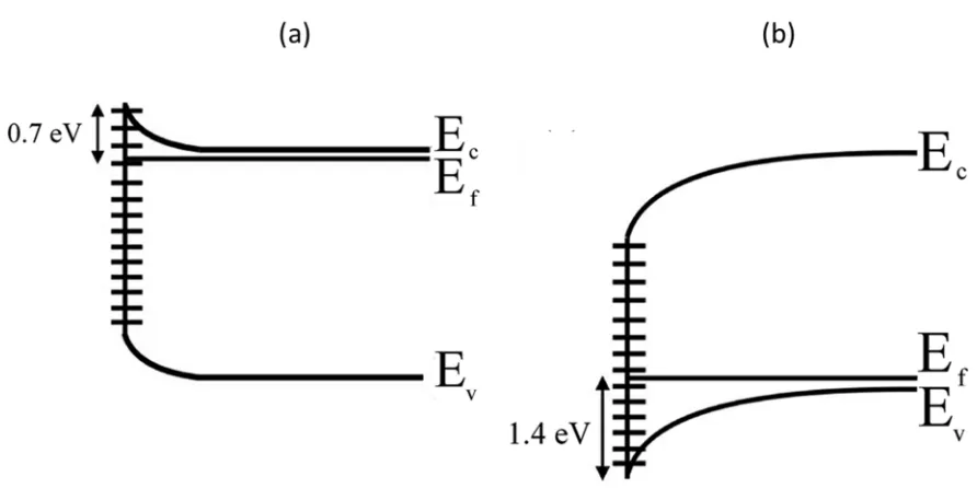
The Fermi level in the bulk n-type GaN is calculated to be near the conduction band for both Ga- and N-polarity. However, the barrier height at CNL for the Ga-polar surface is ≈ 0.7 eV, i.e., the Fermi level is pinned at 0.7 eV below the conduction band and indicates an upward band bending at the surface as shown in Figure 2-3(a). This agrees well with I-V and C-V measurements reported in literature for various metals.107–109 The barrier height surprisingly decreases to zero on N-polar GaN. This is clearly corroborated by recent observations of increased leakage current in the presence of inversion domains in Ga-polar GaN and such domains being used in engineering Ohmic contacts on GaN.110 An intermediate barrier height (≈0.4 to 0.45 eV) has been reported for non-polar a-plane n-type GaN.111 Additionally, in p-type GaN the CNL is observed at 1.4 eV above the VBM implying a downward band bending illustrated in Figure 2-3(b).
/
Figure 2-3: Surface state initiated band bending at the surface in Ga-polar, n-type (a) and
p-type (b) GaN.
Similarly, in both doped epitaxial and insulating bulk AlN samples, the barrier height is the smallest on the N-polar surface and increases from the –c-plane to m-plane by ≈ 0.1 to 0.2 eV and from m-plane to +c-plane by about 0.6 eV. The CNL and barrier height measurements on both doped epitaxial films and insulating substrates are similar within measurement errors as shown in
the N-polar surface. The charging of surface states due to polarization and the effect on surface Fermi level pinning in AlN is illustrated in Figure 2-4. The charge neutrality condition is given by91
sp eDs
(2.4)
where Δϕ is the change in barrier height due to difference in polarization charge between polar and non-polar surfaces, σsp is the polarization charge and Ds is the density of surface states. Theoretically Ds is given by
2 0 20.3 1
1/ 2
s
D
e q
, (2.5)
whereis the high frequency dielectric constant, e is the electron charge and 1/2q represents the decay length.
Figure 2-4: Increased CNL on a) c-plane due to positively charged surface states in
Table 2-2: The measured positions of the Fermi level at the surface (CNL) and barrier heights
(φb) in AlN epitaxial films and substrates
Epitaxial films
Surface Doping type n (cm-3) Ef (eV) (in bulk) CNL (eV) n b (eV)
Al-polar n ≈ 1015 5.8 3.3 2.7
N-polar - - - 4.1 1.9
Substrate
CNL (eV) n
b
(eV)
Al-polar 3.3 2.7
m-plane 3.9 2.1
N-polar 4.0 2.0
~2.5 eV and <1.3 eV after Ga adsorption has also been reported and may be indicative of the observed Ga rich stoichiometry.114
Table 2-3: Experimental and theoretical values for density of surface states (Ds), branch point
energies, spontaneous polarization charge (σsp) and barrier shift (Δφ) in AlN and GaN.
Parameter GaN AlN
σsp (electron-charge cm-2) 2.125x10¹³[7] 5.625x10¹³ [7]
ε∞ 5.35 74 4.6 74
1/2q (nm) 0.186 104 -
Theory Expt Theory Expt
Ds (eV-1cm-2) 2x10¹⁴ 7x10¹³ 1x10¹⁴ 9x10¹³
Δφ (eV) 0.2 0.3 0.5 0.6
BPE (eV) 2.37 115 3 3.33 115 3.9
our conclusions on the energies of acceptor states significantly. However, the reported temperature dependence of p-type pinning116 could be a consequence of acceptor states being induced by adatoms/ surface defects and the density of such defects being a function of temperature.
The surface state decay length is unavailable for AlN and the value of GaN is used. It should be noted that the experimental values for density of surface states in AlN agree well with theoretical calculations on c- and m-planes. The similar CNL on planes of different polarities in GaN and AlN suggest a metallic type partially filled surface states. DFT calculations by Miao et al.118 suggest that surface reconstruction with metallic adlayers is energetically favorable under Al rich conditions in AlN and are expected to exhibit similar surface Fermi level positions at m- and c-planes at ≈ 3.6 to 3.7 eV with the N-polar surface at a lower 3.3 eV when neutral.
pinning. Our experimental results (3.9 eV) seem to be consistent with the metal adlayer hypothesis and clearly explain the lower shift between N-polar and m-plane Fermi level positions. If one assumes that the N-polar CNL is lower by 0.4 eV w.r.t that at m-plane, the surface states fill up with a compensating negative charge as previously explained pushing up the Fermi level by ≈ 0.5 to 0.6 eV to a position slightly above m-plane. Additionally similar slope parameters in barrier height measurements on surfaces of different polarities120 also imply similar surface state densities and justify the assumptions in this work. The metallic surface electronic structure and CNL positions also corroborates with the requirements of 2DEG formation in HEMTs.118 It has to be noted that O-induced defects on the surface may also introduce states and may be partly responsible for the pinning. Consequently, surface passivation of GaN and AlN must reduce mid-gap surface states and interfacial oxygen and compensate the surface polarization charge as well and is discussed in chapter 6.
2.5 Polarization charge compensating surface states and electron
affinity
The direction of the surface dipole between charged surface states and polarization charge in GaN may be determined from electron affinity (EA) measurements. The effect on electron affinity at the surface by the dipole is illustrated in Figure 2-5. It has been reported that electron affinity on N-polar GaN is a few eV lower than that of Ga-polar GaN.90 The dipole voltage drop is calculated by:
spd
q V
C
Assuming the width of the dipole, d, is of the order of the decay length of surface states (0.2 nm), the potential drop across the dipole is ≈1 eV. The difference in EA is given by:
2 V 2eV
, (2.7)
where V is the dipole potential drop. The opposite band bending at the surface of metal polar and N-polar surfaces could induce further difference in electronegativity. The change in EA agrees reasonably well with experimentally reported values.90
This work provides several useful implications on Schottky and Ohmic contacts on GaN, AlN and AlGaN and their dependence on doping and polarity. For example, N-polar and non-N-polar surfaces are most suitable for Ohmic contacts due to lower barrier heights.
Figure 2-5: (a) Decrease in electron affinity on N-polar GaN due to surface dipole and (b)
2.6 Conclusions
3 CHAPTER 3: a surface study of the alloy AlGaN
IntroductionAs described in chapter 2, AlN exhibits a large barrier height at the charge neutrality level (CNL)121 and therefore exhibits large Schottky barriers120 as will be described in chapter 4, making it a promising candidate for high-power Schottky diodes with very low leakage. However, large dopant activation energies and hence the requirement of heavy doping to achieve moderate carrier concentrations is a major challenge in implementing AlN based technology. Relatively poor Ohmic contacts on AlN further limit its applications.122 These challenges can be overcome by alloying AlN with GaN, which sharply reduces the dopant activation energy, even at low Ga concentrations,44 while at the same time maintains many of the advantages of AlN. The performance and behavior of devices based on AlGaN are determined by the surface and interface properties and a better understanding of them could help in predicting, designing, and improving the performance of these surface/interface-based devices.
Growth, sample pretreatment and experimental setup
Epitaxial GaN thin films, AlGaN, and AlN were grown using a vertical, cold-wall, rf-heated, low-pressure metalorganic chemical vapor deposition reactor (MOCVD) on either c-plane sapphire or low dislocation density AlN single crystalline substrates described in chapter 1.29,30,123–125 Trimethylaluminum, triethylgallium and ammonia were used as precursors for Al, Ga and N respectively. Silane and bis-cyclopentadienyl magnesium were used as Si (n-type) and Mg (p-type) precursors respectively. Further details on the growth process can be found elsewhere.58,96,97 Growth is along c-axis and all films studied in this chapter have metal polar surfaces. Post growth surface preparation for surface analysis by XPS included cleaning in organic solvents, a 10-minute treatment in NH4OH at 50°C to reduce surface oxygen,119 and a rinse under deionized water.
X-ray photoelectron spectroscopy (XPS) was the primary characterization tool where all binding energies were measured with respect to the Fermi level and the experimental setup and charge correction techniques are described in chapter 2. The composition of the AlGaN films was determined using an X-ray diffraction (XRD) technique described by Tweedie et al.126 For the XRD measurements, a Philips X’Pert Materials Research Diffractometer with a Cu Kα X-ray source was used.
Surface chemical composition
molar fraction indicates oxygen forming about 1/2 to 3/4 monolayer on all AlGaN surfaces, including GaN and AlN. Oxide/hydroxide formation is not sufficient to explain the metal rich stoichiometry indicating different origin to the metal rich stoichiometry. The influence of the observed metal rich stoichiometry on electronic properties, its origin and role of oxygen is discussed later on in this chapter.
Charge neutrality levels and barrier heights
Figure 3-2 shows the CNL as a function of composition. It is found that the CNL measured with respect to the valence band maximum exhibits nearly linear behavior and could be represented by a linear interpolation between CNLs of GaN and AlN. It is given by
0.8 2.7
CNL x eV (3.1)
The barrier height at the CNL, n b
is the barrier faced by an electron at the surface
Fermi level to enter the conduction band and is given by Eg-CNL. The band gap for AlGaN was calculated assuming a bowing parameter of 1 eV.9,11,128,129 The effect of strain present due to the deposition either on sapphire or AlN substrates is expected to be less than the measurement resolution of 0.2 eV.130 Measured n
b
for various
samples is plotted in Figure 3-2 as a function of Al composition. The barrier height at the CNL shows the Fermi level to be pinned well below the conduction band minimum and, hence, indicates an upward band bending at the surface in Si-doped samples. Due to the nonlinearity associated with bandgap bowing, a linear interpolation cannot represent the barrier height at CNL. An interpolation rule similar to Vegard’s law, but with a bowing parameter equal to that found for the bandgap (~1 eV) is required, i.e., barrier height at the CNL is given by:
22.5 0.7(1 ) 1 (1 ) 0.8 0.7
n
b x x x x x x eV
(3.2)
Further, barrier height at CNL can be approximated by a linear function at very high Al compositions (x>>0.5) given by:
2.5
n
b x
Figure 3-1: Measurement of the CNL using XPS valence band data of (a) Si doped
Al0.85Ga0.15N and (b) Mg doped Al0.7Ga0.3N grown on AlN via comparison with theoretical
VDOS. The dashed and solid lines represent the calculated and Gaussian broadened valence
band density of states and the dots represent the XPS data.
oxide stoichiometry, metal adlayer/bilayer type surface reconstruction is most likely present at surface of AlGaN. As discussed earlier, the origins of metal rich stoichiometry may lie in the surface reconstructions. This is in agreement with XPS studies on AlN121 discussed in chapter 2 which also implied an existence of such reconstructions.
Figure 3-2: CNL and barrier heights at the CNL as a function of Al composition AlGaN grown
on AlN and sapphire. 25% and 40% AlGaN are unintentionally doped. Mg doped (75%) AlGaN
is grown on AlN. The rest are Si doped. Dashed lines are interpolations between AlN and
GaN.
Surface work function and electron affinity of AlGaN
binding energy measured with respect to the Fermi level is expected to change if the Fermi level shifts within the bandgap.132 Interestingly, the core level binding energies of Ga 3d and Al 2p measured with respect to the Fermi level by XPS were found to be independent of the composition (standard deviation is ~0.2 eV, and the measurement resolution is ~0.2 eV) as shown in Figure 3-3. Consequently, it may be concluded that the energy difference between surface Fermi level and vacuum level, i.e., surface work function remains constant with composition.
Figure 3-3: Binding energies of Al 2p and Ga 3d core levels as a function of AlGaN
composition in films that were grown on AlN single crystalline substrate and sapphire. 25%
and 40% AlGaN are unintentionally doped. Mg doped (75%) AlGaN is grown on AlN. The rest
are Si doped.
In addition, knowledge of conduction band referenced to the Fermi level, i.e., Φ
allows us to estimate the change in electron affinity (χ) with Al composition as:
( ( )n n(0))
AlGaN GaN b x b
Hence, the electron affinity is directly correlated to Φ and is given by
2 0.8
AlGaN GaN x x
. This indicates a difference in electron affinity of ~1.8 eV
between AlN and GaN and agrees well with experimental reports of electron affinities of around 3 eV and 1eV for GaN133–135 and AlN,136–138 respectively. This difference is slightly lower than the 2.5 to 3 eV reported by Grabowski et al.,134 however, it is not surprising considering the variation in electron affinity values in literature, possibly due to variations in polarization induced dipoles at the surface.121
deduced band structure as a function of Al composition is shown in Figure 3-4, assuming surface Fermi level as the reference energy.
Band offsets in ALGaN
The CNL is assumed to be strongly correlated to the BPE and determines the valence and conduction band offsets at heterojunctions according to IFIGS model.143 The effect of the interface dipole is typically neglected for semiconductor-based heterojunctions since semiconductors tend to exhibit similar electronegativities.143 Furthermore, our earlier analysis on electron affinity directly correlated to CNL via Φ
ensures the same band offsets even if Anderson’s rule is employed. The band offsets at AlxGa1-xN/AlyGa1-yN are hence estimated as
2 2 0.8
C
E x y x y
eV (3.5)
and EV 0.9
x y
eV (3.6)offset ratios of ~0.7/0.3 from DFT calculations and experimental results at AlN/GaN interface144,145 and low ratios of 0.5/0.5–0.6/0.4 at AlGaN/GaN interfaces with low Al compositions.146 Equations (3.5) and (3.6) represented in Figure 3-5 provide a useful tool for designing AlGaN heterostructures since band offsets play an important role in carrier confinement and emission wavelengths in LEDs and laser diodes.
Figure 3-4: The band divergence in AlGaN as a function of composition determined using
CNL, barrier height at CNL and the constant work function of 3.7 eV. (Dashed lines represent
the interpolations)
Conclusion
of the bandgap difference, respectively. Characterization of core level binding energies revealed a composition independent surface work function. Consequently, the electron affinity was found to be a linear function of the barrier height at CNL, i.e., band offsets determined via IFIGS and Anderson’s rule were found to be identical. The bowing in the dependence of Φ on Al composition resulted in an increase and decrease in the ratio of conduction band offset to bandgap difference in AlN/AlGaN and GaN/AlGaN interfaces respectively. Our results also indicate that the origin of the bandgap bowing is in the conduction band.
Figure 3-5: Conduction band offset (ΔEc), as a function of Al composition of the two layers
forming the heterojunction. The dependence of the ratio of conduction band offset and valence
4 CHAPTER 4: Schottky contacts on AlN and Al rich AlGaN
IntroductionAlN and Al rich AlGaN based Schottky diodes are expected to have several advantages over other diodes based on typical wide bandgap semiconductors such as SiC. These advantages include high reverse breakdown voltage, low leakage current, and high operation power as evidenced by the Baliga figure of merit of 876 GW/cm2, or nearly 200 times the value for SiC as discussed in chapter 1.2 Applications for these devices include high-power switches and frequency multipliers.3,87 Schottky and Ohmic contacts on GaN and AlGaN with low Al composition (< 30%) have been reported extensively in literature.2,3,88,147,148 However in AlN and AlGaN with high Al compositions (> 70%), Schottky barriers present a difficult study due to non-ohmic back contacts with very high contact resistivity and large sheet resistances.88 The presence of Fermi level pinning and surface states at the surface of AlN and AlGaN have been previously discussed (chapters 2 and 3) and these factors are expected to influence Schottky barrier formation. In this chapter, a study of the formation of Schottky barriers for various metals on surfaces of different polarities of AlN via the X-ray photoelectron spectroscopy (XPS)-based contactless procedure is reported and a model developed. Further, the model is extended to Al rich AlGaN and is corroborated by current-voltage and capacitance-voltage measurements. The Schottky barrier height is determine
![Figure 1-1: Unit cell of GaN with [1 0 0] perpendicular to plane of paper.](https://thumb-us.123doks.com/thumbv2/123dok_us/1194058.1149965/26.612.222.410.69.361/figure-unit-cell-gan-perpendicular-plane-paper.webp)
![Figure 1-4: The crystal structure of sapphire with [100] perpendicular to plane of paper](https://thumb-us.123doks.com/thumbv2/123dok_us/1194058.1149965/33.612.106.520.186.418/figure-crystal-structure-sapphire-perpendicular-plane-paper.webp)