ABSTRACT
JUVEKAR, SWANAND. A Fast Acting DC Solid State Circuit Breaker. (Under the direction of Dr. Subhashish Bhattacharya).
The thesis focuses on developing a low voltage prototype of a medium voltage DC
solid state circuit breaker. Various topologies of DC solid state breakers are evaluated and
the one suitable to implement a fast acting fault interrupting device is chosen. Simulations
are performed using MATLAB/PLECS to verify desired system operation with chosen
components. The circuit is then implemented in hardware using a MOSFET semiconductor
switch and a micro-controller to control its operation. Hardware backup circuitry is also
implanted using OPAMP. The maximum operation time for hardware developed in this
thesis is 4.042uS. Initial testing is carried out at low voltage (60V) and testing waveforms are
presented along with explanation of different times. Firmware logic is also explained with a
flowchart. Later, the hardware is tested at 400V and testing results are presented.
A mathematical expression for sensor operating time is derived and simulation for the
same is also presented to verify calculated time. Limitations of present hardware are
explained by comparing calculated operation time and obtained hardware results. Later,
SPICE simulations are performed on 7.5kV DC system to evaluate and compare performance
of 6.5kV Si-IGBT and SiC- MOSFET. The tradeoff between the two is also explained which
© Copyright 2011 by Swanand Juvekar
A Fast Acting DC Solid State Circuit Breaker
by
Swanand Juvekar
A thesis submitted to the Graduate Faculty of North Carolina State University
in partial fulfillment of the requirements for the degree of
Master of Science
Electrical Engineering
Raleigh, North Carolina
2011
APPROVED BY:
_______________________________ ______________________________
Dr. Subhashish Bhattacharya Dr. Mesut Baran
Committee Chair
ii
DEDICATION
To My Parents,
Ramkrishna Hari Juvekar AND
iii
BIOGRAPHY
The author, Swanand Juvekar was born on October 31, 1985 in Mumbai, India. He
completed high school education from Balmohan Vidyamandir, Mumbai in March 2001. He
received Bachelor of Engineering degree from (V.J.T.I) University of Mumbai in 2007
specializing in Electrical Engineering. He started pursuing graduate studies at North Carolina
State University in Fall 2009 and since then he has been working at Future Renewable
Electric Energy Delivery and Management (FREEDM) Systems Center under the guidance
iv
ACKNOWLEDGMENTS
I would like thank my adviser, Dr. Subhashish Bhattacharya for his guidance, support
and encouragement. I have learnt a lot of new things while working with him on different
projects. I have benefited greatly by being a student at FREEDM center where I got
opportunity to do innovative research and to interact with brilliant individuals. I would like to
thank Dr. Kamalesh Hatua, a postdoctoral researcher at FREEDM center for the insights I got
in power electronics through discussions with him.
I would also like to thank my friends Arun Kadavelugu and Sumit Dutta who have
provided their valuable inputs through engaging discussions. I would like to thank my friends
Siddharth Ballal, Mihir Shah, Hesam Mirzaee, Shailesh Notani, Vijay Shanmugasundaram,
Ankan De, Nicholas Parks, Arvind Govindaraj and Shashank Bodhankar. I appreciate the
help provided by staff members at the center, especially Karen Autry and Hulgize Kassa for
the facilities and support in the lab.
I would also like to thank my friends Mrunal Sabnis, Anish Karandikar, Ameya Pitre,
Shrikant Chaudhari, Nilesh Gavaskar, Ashwin Mayya, Yatin Patil, Lakshmikant Agarwal and
Abhijeet Kothawade for making my stay at NC State University a memorable journey.
Finally, I want to thank my parents Ramkrishna Juvekar and Sanjeevani Juvekar for
their love, care and constant encouragement. This work would not have been possible
v
TABLE OF CONTENTS
LIST OF FIGURES ... vii
CHAPTER 1 Solid state circuit breakers for DC applications ... 1
1.1 Motivation...2
1.2 Background of DC SSCBs...7
1.3 Scope of thesis ...10
1.4 Overview of chosen SSCB topology ...11
CHAPTER 2 PLECS simulations of SSCB system... 13
2.1 SSCB components ...13
2.2 Calculation of operation time...14
2.3 System simulation at 400V DC...15
2.4 Simulation results...16
CHAPTER 3 Hardware implementation and testing results... 20
3.1 SSCB hardware...20
3.2 Firmware logic ...23
3.3 Hardware testing results at 60V ...25
3.3.1 Case 1: Current threshold=2.7A ... 25
3.3.2 Case 2: Current threshold=5.5A ... 33
3.3.3 Case 3: Current threshold=8.1A ... 40
3.4 Hardware testing results at 400V...47
CHAPTER 4 Prediction of sensor operation time ... 53
4.1 Mathematical derivation for sensor response time ...53
4.2 Calculation of sensor response time ...55
vi
4.2.2 Case 2: Current threshold=5.5A ... 56
4.2.3 Case 3: Current threshold=8.1A ... 57
4.3 Simulation to verify sensor response time ...57
CHAPTER 5 SPICE simulations of 7.5kV DC system ... 63
5.1 System description ...63
5.2 Simulation results with Si-IGBT ...65
5.3 Simulation results with SiC MOSFET...73
5.4 Conclusions and future work ...81
CHAPTER 6 Improved PV model for faster response ... 83
6.1 Model for a solar cell ...83
6.2 Solar panels and solar arrays...86
6.3 Important Factors affecting panel performance ...88
6.4 Spreadsheet analysis for calculating I-V curves ...90
6.5 Development of a PV model...92
vii
LIST OF FIGURES
CHAPTER 1 ... 1
Figure 1.1 FREEDM system single line diagram [3] ...3
Figure 1.2 Typical naval MVDC system...5
Figure 1.3 7.5kV DC system ...5
Figure 1.4 The 400V DC testbed developed as prototype of MVDC [5] ...6
Figure 1.5 Hybrid DC circuit breaker [6]...7
Figure 1.6 DC circuit breaker scheme employing VSC as crowbar [8]...8
Figure 1.7 DC circuit breaker scheme employing forced commutation technique [9] ...9
Figure 1.8 DC solid state circuit breaker [10] ...9
Figure 1.9 Block diagram of SSCB system...11
CHAPTER 2 ... 13
Figure 2.1 SSCB circuit diagram ...16
Figure 2.2 SSCB simulation waveforms ...17
Figure 2.3 Zoomed view of waveform when fault occurs ...19
CHAPTER 3 ... 20
Figure 3.1 The block diagram of SSCB system ...21
Figure 3.2 The block diagram of SSCB system ...22
Figure 3.3 Test setup for 60V testing ...23
Figure 3.4 SSCB firmware logic flowchart...24
Figure 3.5 SSCB system operation at 2.7A threshold...26
Figure 3.6 First step, total time (Threshold=2.7A) ...26
Figure 3.7 First step, micro-controller and sensor circuitry time (Threshold=2.7A)...27
Figure 3.8 Second step, total time (Threshold=2.7A) ...28
viii
Figure 3.10 Third step, total time (Threshold=2.7A) ...30
Figure 3.11 Third step, micro-controller and sensor time (Threshold=2.7A)...30
Figure 3.12 Fourth step, total time (Threshold=2.7A) ...31
Figure 3.13 Fourth step, micro-controller and sensor time (Threshold=2.7A) ...32
Figure 3.14 SSCB system operation at 5.5A threshold...33
Figure 3.15 First step, total time (Threshold=5.5A) ...34
Figure 3.16 First step, micro-controller and sensor circuitry time (Threshold=5.5A)...34
Figure 3.17 Second step, total time (Threshold=5.5A) ...35
Figure 3.18 Second step, micro-controller and sensor time (Threshold=5.5A) ...36
Figure 3.19 Third step, total time (Threshold=5.5A) ...37
Figure 3.20 Third step, micro-controller and sensor time (Threshold=5.5A)...37
Figure 3.21 Fourth step, total time (Threshold=5.5A) ...38
Figure 3.22 Fourth step, micro-controller and sensor time (Threshold=5.5A) ...39
Figure 3.23 SSCB system operation at 8.1A threshold...40
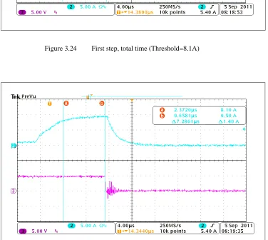
Figure 3.24 First step, total time (Threshold=8.1A) ...41
Figure 3.25 First step, micro-controller and sensor circuitry time (Threshold=8.1A)...41
Figure 3.26 Second step, total time (Threshold=8.1A) ...42
Figure 3.27 Second step, micro-controller and sensor time (Threshold=8.1A) ...43
Figure 3.28 Third step, total time (Threshold=8.1A) ...44
Figure 3.29 Third step, micro-controller and sensor time (Threshold=8.1A)...44
Figure 3.30 Fourth step, total time (Threshold=8.1A) ...45
Figure 3.31 Fourth step, micro-controller and sensor time (Threshold=8.1A) ...46
Figure 3.32 SSCB board in 400V DC testbed developed as prototype of MVDC [5]...47
Figure 3.33 SSCB system operation at 5.5A threshold, 400V ...49
Figure 3.34 First step, total time at 400V(Threshold=5.5A)...49
Figure 3.35 Second step, total time at 400V (Threshold=5.5A) ...50
Figure 3.36 Third step, total time at 400V (Threshold=5.5A) ...51
ix
CHAPTER 4 ... 53
Figure 4.1 Simulation of circuit to measure current sensor response time ...58
Figure 4.2 current sensor response time for 2.7A threshold ...59
Figure 4.3 Current sensor response time for 5.5A threshold...60
Figure 4.4 Current sensor response time for 8.1A threshold...61
CHAPTER 5 ... 63
Figure 5.1 7.5kV DC system circuit diagram...64
Figure 5.2 Simulation results with Si-IGBT ...65
Figure 5.3 Zoomed in results with Si-IGBT...66
Figure 5.4 VCE voltage variation with Si-IGBT ...67
Figure 5.5 Steady state VCE with Si-IGBT ...67
Figure 5.6 Zoomed in results with Si-IGBT (50nS delay) ...68
Figure 5.7 VCE voltage variation with Si-IGBT (50nS delay) ...69
Figure 5.8 Steady state VCE with Si-IGBT (50nS delay)...70
Figure 5.9 Zoomed in results with Si-IGBT (150nS delay) ...71
Figure 5.10 VCE voltage variation with Si-IGBT (150nS delay) ...72
Figure 5.11 Steady state VCE with Si-IGBT (150nS delay)...72
Figure 5.12 Simulation results with SiC-MOSFET ...73
Figure 5.13 Zoomed in results with SiC-MOSFET ...74
Figure 5.14 VDS voltages variation with SiC-MOSFET...75
Figure 5.15 Steady state VDS with SiC-MOSFET ...75
Figure 5.16 Zoomed in results with SiC-MOSFET (50nS delay)...76
Figure 5.17 VDS voltage variation with SiC-MOSFET (50nS delay)...77
Figure 5.18 Steady state VDS with SiC-MOSFET (50nS delay)...77
Figure 5.19 Zoomed in results with SiC-MOSFET (150nS delay) ...78
Figure 5.20 VDS voltage variation with SiC-MOSFET (150nS delay)...79
x
CHAPTER 6 ... 83
Figure 6.1 Model of a solar cell [13]...84
Figure 6.2 I-V Characteristics of a solar cell...85
Figure 6.3 Deriving I-V Characteristics of a solar panel from cell I-V characteristics [13].86 Figure 6.4 A solar cell, PV panel and an array [13] ...87
Figure 6.5 Entech terrestrial solar array [14] ...87
Figure 6.6 I-V Characteristics of a solar panel at different isolations [13] ...88
Figure 6.7 I-V Characteristics of a solar panel at different cell temperatures [13] ...89
Figure 6.8 I-V Characteristics of REC215 AE-US obtained using spreadsheet ...92
Figure 6.9 I-V Characteristics of REC215 AE-US from datasheet...92
Figure 6.10 Simulation for PV model comparison...94
Figure 6.11 ICCS model response...95
Figure 6.12 Zoomed ICCS model response ...96
Figure 6.13 VCCS model response ...97
1
CHAPTER 1
Solid state circuit breakers for DC applications
A circuit breaker (CB) is a kind of switch which is supposed to operate whenever
there is a fault condition or sustained overloads in power system. Primary function of a
circuit breaker is to isolate the faulty section of the power system thereby protecting the loads
and system itself from damage due to excessive currents. There exist different types of circuit
breakers such as thermal circuit breakers, electromagnetic circuit breakers, thermal/magnetic
circuit breakers and solid state circuit breakers. All of these differ in principle of operation.
Thermal circuit breakers use a bimetallic strip which bends due to heat produced by
excessive current during fault condition. As a result, the current carrying contact open up
breaking the main circuit. In electromagnetic type circuit breakers, main current flows
through a coil which produces magnetic field to attract an armature. When current is higher
than set value, magnetic field becomes strong enough to pull the armature thereby breaking
the main circuit. Circuit breakers combining both of these effects are called thermal/magnetic
circuit breakers. These use electromagnetic action to provide over-current protection and
thermal effect to provide protection against sustained overloads.
Thermal circuit breakers have long tripping times which means fault current
continues to flow through the system longer which could be dangerous to the system and
2
electromagnetic CBs are faster than thermal CBs, their tripping speed is not sufficient to
protect modern loads which are very sensitive to extreme electrical conditions. Again these
are sensitive to external magnetic interference and vibrations in addition to ambient
temperature [1]. A solid state circuit breaker scores over other types mainly because of its
faster tripping times with additional advantages including soft start, soft turn off, reduced
switching surges, high reliability and longer life due to lesser wear and tear (no arcing),
improved power quality at healthy section of system [2].
1.1 Motivation
Figure 1.1 on next page shows a single line diagram of FREEDM system. The IFM
(Intelligent Fault Management) systems are implemented using SSFID (Solid State Fault
Isolation Devices). The function of SSFID is to isolate the faulty section of the system
thereby allowing rest of the system to function normally. The motivation for work presented
in this thesis is to develop a MVDC counterpart of SSFIDs used in MVAC system which is
part of FREEDM grid.
Recently medium voltage DC (MVDC) distribution is becoming more and more
popular. Advantages of MVDC distribution include higher power transfer capability,
transformer size reduction due to high frequency operation, higher power density and
potentially higher efficiency, ease of paralleling generating units, better fault controllability
and simpler cabling. As a result, MVDC systems are being proposed for wind farms, large
3
Figure 1.1 FREEDM system single line diagram [3]
Modern navy warships are becoming more and more electric and nature of loads on
board is changing from energy intensive to power intensive. Therefore, it is becoming
increasingly challenging to supply ship’s power demand with limited available space. The
obvious solution to this problem is to increase the ship power density. In the first attempt to
tackle this issue, Integrated Power System (IPS) was proposed meaning a shared electric
power generation for all types of ship electric load. This was in contrast to the inefficient
traditional approach of having dedicated generation for both propulsion and ship service
4
(MVAC) distribution system, which has been used for many years on navy ships, falls short
of answering these soaring power demands due to its bulky infrastructure mainly consisting
of huge high power 60Hz three-phase transformers. This limits the usability of MVAC
system for modern navy warfare ships which are geared toward more advanced electric type
of loads. Considering the major issue of power density with future combatant ships, the Next
Generation Integrated Power system (NGIPS) roadmap [4], developed by the Electric Ship
Office (ESO) of Office of Naval Research (ONR), suggests the Medium Voltage DC
(MVDC) distribution as a viable solution to increase power density on the ship [5]. One such
system is shown in figure 1.2 [5] below. The figure shows a typical naval MVDC system
with several power sources and several loads. The power required for loads like proposer,
weapon systems etc could be derived from a generator, fuel cell, batteries and so on. As in
case of any power system, the system and loads need to be protected from faults and here we
need a MVDC circuit breaker. Figure 1.3 shows a scaled down version MVDC system shown
in figure 1.2. In figure 1.3 [5], a 3-phase AC source is feeding a transformer which scales
down its input voltage to 4.16kV. A power electronic converter is acting as a rectifier and
generates 7.5kV DC at the output. Different loads are hanging off the DC bus and as shown
in figure 1.3, SSCB could be used to provide overcurrent protection to loads connected to its
output. To serve as a proof of concept, a low voltage (400V) prototype of MVDC circuit
5
Figure 1.2 Typical naval MVDC system
6
As a part of ongoing research on MVDC, a 400V DC testbed is being developed in
FREEDM systems center. The 400V system is shown in figure 1.4. It can be seen that there
are several loads connected to DC bus some of which could be sensitive loads which need
faster fault isolation in order to protect them from damage. In a real MVDC system, fault
severity could be even higher owing to higher bus voltage. This thesis focuses on developing
DC solid state circuit breaker hardware for 400V system shown in figure 1.4. Simulations are
also performed for a 7.5kV MVDC system using different devices and results are compared.
7
1.2 Background of DC SSCBs
In literature, hybrid circuit breakers were proposed as a solution to high conduction
losses due to higher on resistance of a semiconductor switch [6]. In such a configuration,
fault current is interrupted in multiple steps as described in [7]. Normally, load current would
flow through mechanical switch and only when fault occurs, the semiconductor switches are
fired to divert fault current away from mechanical switch and allow opening it without any
arcing. With advances in power semiconductor technology, new and better devices like
IGBTs, SiC MOSFETS etc were developed which have much superior performance as
compared to their ancestors. Recently, MOSFETS having on resistance as small as 19mΩ
(e.g. STY112N65M5) have arrived in market. This eliminates the need to use mechanical
switch in order to reduce conduction losses and thus reduces size and cost.
8
With current technology, there are three approaches to implement the DC solid state
fault interrupting scheme. Conventional approach makes use of an ability of VSC to act as a
crowbar circuit and AC side circuit breaker interrupts fault current as described in [8]. This is
shown in figure 1.6. Another method is to use a SCR based switch with forced commutation
circuit which is required to turn SCR off in case of fault as described in [9]. This is shown in
figure 1.7. Third method uses a semiconductor device like IGBT or MOSFET having
controlled turn off capabilities since current limiting action needs to be faster than a
half-cycle as described in [10]. This is shown in figure 1.8.
9
Figure 1.7 DC circuit breaker scheme employing forced commutation technique [9]
10
In the first case, speed of fault interruption depends on AC side circuit breaker which
might not meet the requirements and moreover VSC switches need to withstand full fault
current until the breaker interrupts it. Last approach simplifies the hardware implementation
by allowing use of a simpler power circuit and also allows ultra fast operation. Therefore,
this approach is focused on for purpose of hardware implementation.
1.3 Scope of thesis
The most important aspect focused on in this thesis is speed of operation. Current
literature shows this time to be several tens or hundreds of micro-seconds. An existing patent
[1] with same topology as chosen for this thesis mentions time required to inhibit fault
current as 300uS. Similar system as shown in [10] shows hardware results with operation
time more than 15uS. This thesis aims at developing SSCB hardware with operation time in
less than 5 microseconds using silicon MOSFET.
In section 1.4, topology of SSCB implemented in this thesis is described. In next few
chapters, MATLAB/PLECS simulations are performed for 400V DC system and events
occurring during turn on and turn off of switch are explained. The chosen SSCB topology is
realized in hardware and hardware testing waveforms are presented with explanation of
different times. Later, analysis is performed to calculate sensor response time and simulation
is performed with models of actual components used for hardware implementation to verify
the result obtained by calculations. Finally, simulations are also performed for 7.5kV MVDC
11
results for different devices to show tradeoff between them to be considered while choosing
the right switch for SSCB. In final section of thesis, a new PV model is developed which acts
as impedance dependent current source rather than conventional voltage controlled current
source. The benefits of new model are explained with the help of MATLAB/PLECS
simulation.
1.4 Overview of chosen SSCB topology
12
The figure 1.9 shows the block diagram of SSCB system developed in this thesis. The
micro-controller is central decision making unit. It is continuously monitoring response of
current sensor for overcurrent condition. In normal condition, micro-controller commands
gate driver to keep the semiconductor switch ON. When a fault occurs, load current begins to
increase at a rate determined by fault current limiter. The fault current limiter is an inductive
element which limits di/dt in case of fault. To avoid having over-voltage stresses on
semiconductor switch, a freewheeling path must be provided at the time of current
interruption by semiconductor switch. Once current crosses a threshold programmed in
controller, it commands gate driver to shut the semiconductor switch off. Since
micro-controller is a programmable device, logic for auto-reclosure can also be implemented. If the
fault is persistent after 3 attempts, the main switch will be turned off by micro-controller and
will remain off until reset manually. Once the fault is cleared, micro-controller sends signal
to trip indicator circuit which lights an LED and sends signal to other circuits. In case
micro-controller fails to act in timely manner, a hardware backup circuitry with current threshold
higher than that of micro-controller comes into action. This hardware backup uses reliable
OPAMP circuitry to compare current sensor response with a fixed threshold and send trip
13
CHAPTER 2
PLECS simulations of SSCB system
In this chapter, SSCB topology described in chapter 1 is simulated using
MATLAB/PLECS software to study its operation. Components to be used in hardware
implementation are chosen and real values of device parameters are used for simulation.
Parasitic elements are also introduced to make simulation more realistic. Various delays and
operation times of individual components are calculated and modeled in the simulation. A
calculation for expected total operating time is also performed.
2.1 SSCB components
The semiconductor switch used for hardware implementation is a STW55NM60ND
MOSFET with typical on-resistance of 47mΩ. The micro-controller used is PIC16F690 and
is operated with 20MHz crystal. Gate driver is implemented using IXDN409SI which is a
high speed, high current gate driver chip designed to drive a switch at faster rate. An
opto-coupler (HCNW2211) is also used to provide isolation upto 5kV. Current sensor used is
LA-55P which is closed loop current transducer working on Hall Effect principle. Output of
current sensor is fed to micro-controller through an OPAMP (TLE2142I) buffer. Fault
14
diode (DSEP29-06A) is used to provide a freewheeling path to inductor current when main
switch opens.
2.2 Calculation of operation time
Quite a few components contribute to total operation time of SSCB. After load
current crosses threshold, current sensor output takes some time to change to that
corresponding to overcurrent condition followed by OPAMP buffer operation time. Output of
OPAMP buffer is fed to comparator inside micro-controller which has its own response time
followed by time taken by firmware to execute the overcurrent trip logic. When
micro-controller sends a turn off command to main switch, it has to pass through opto-coupler and
gate driver. Finally, the semiconductor switch itself takes finite time to turn off whose value
depends on gate resistance. Time taken by individual components is obtained from datasheet
and is listed below.
• LA55-P, Current sensor: 1uS (From datasheet)
• TLE2142I, OPAMP buffer: 340nS (From datasheet)
• Comparator inside micro-controller: 400nS (From datasheet of PIC16F690)
• Micro-controller logic: 9*0.2uS = 1.8uS (9 instructions each taking 200nS)
• HCNW2211, opto-coupler: 160nS+7nS=167nS (OFF propagation delay + Fall time)
15
• STW55NM60ND, MOSFET: 284nS (OFF propagation delay + Fall time)
From above mentioned individual operating times, operating times of different
sections of circuit and total operation time is calculated as follows.
• Adding all individual operating times of components, expected total maximum
operating time = 4.042uS.
• Maximum operating time for sensor, OPAMP and micro-controller
1uS+0.34uS+0.4uS+1.8uS= 3.54uS.
• Maximum operating time for opto-coupler, gate driver and switch to turn off is
0.167uS+0.051uS+0.284uS=0.502uS=502nS.
2.3 System simulation at 400V DC
Figure 2.1 shows the circuit diagram of the SSCB system. It has a 400V DC stiff
input and it is feeding a load of 85.5ohm. Main power switch which carries load current and
interrupts it in case of fault is a MOSFET (STW55NM60ND). Inductor L2 is acts as a fault
current limiter which will limit source current di/dt when fault occurs. Operating times of
various devices are modeled and are as shown in figure. L3 and L4 are used to model
parasitic inductances in circuit. Waveforms obtained from simulation are presented in next
16
Figure 2.1 SSCB circuit diagram
2.4 Simulation results
Figure 2.2 below shows simulation waveforms. At the start of simulation, main
switch is kept off. As a result it is blocking 400V across it and no power is delivered to load.
At t=50e-6, turn on gate signal is given to main switch and it begins to conduct current equal
17
18
At t=80e-6, a 25ohm load bank is switched in parallel with existing load. As a result
total load resistance becomes 25//85.5 = 19.344ohm which means steady state fault current
will be 400/19.334 = 20.68A if no action is taken. As seen in figure 2.1, overcurrent
threshold is set at 5.5A. The control circuitry will start taking action after it detects
overcurrent which happens 1.34uS (sensor circuitry response time) after current crosses
5.5A. Fault current continues to increase till it is interrupted by main switch after 4.042uS
from the instant fault current crosses the threshold. When the fault current is interrupted,
inductor current freewheels through diode and main switch blocks 400V. Zoomed in view of
figure 2.2 is shown in figure 2.3 on next page.
After auto-reclosure delay of 50uS, control circuitry attempts to power up the load
and check if fault is still present. As the fault is still there, current through load starts rising at
a rate determined by inductor. Again control circuitry begins to take action 1.34uS after fault
current crosses the threshold and fault current in interrupted after about 4.042uS. This
process repeats two more times and then firmware concludes that it is a permanent fault and
keeps main switch open until micro-controller is reset manually. Zoomed in version of
waveform is shown below which shows fault being interrupted 4.042uS after fault current
19
20
CHAPTER 3
Hardware implementation and testing results
The topology chosen for SSCB implementation is shown in figure 1.9 and its working
is explained in chapter 1. This chapter elaborates on hardware implementation of low voltage
prototype SSCB for 400V DC testbed. Firmware logic for micro-controller is explained with
a flowchart. The hardware is first tested at low power for purposes of firmware development
and testing results are presented. Later, it is tested at 400V and captured waveforms are
presented in this chapter with explanation of different times.
3.1 SSCB hardware
For convenience, figure 3.1 again shows the block diagram of chosen SSCB
topology. This can be compared to actual hardware pictures shown later to see how each
block in the system got translated into real hardware. As mentioned in previous chapter, the
semiconductor switch used is a MOSFET (STW55NM60ND) with typical on-resistance of
47mΩ. The micro-controller used is PIC16F690 and is operated with 20MHz crystal. Gate
driver circuitry is implemented using IXDN409SI which is capable of supply driving currents
as high as 9A. An opto-coupler (HCNW2211) is also used to provide isolation upto 5kV.
Current sensor used is LA-55P which is closed loop current transducer working on Hall
21
(TLE2142I) buffer. Fault current limiter is simply an inductor which limits di/dt when fault
happens. A freewheeling diode (DSEP29-06A) is used to provide a freewheeling path to
inductor current when main switch opens.
Figure 3.1 The block diagram of SSCB system
Figure 3.2 shows picture of SSCB board. The main switch (MOSFET) is placed
upside down and hence only its terminals are visible in figure 3.2. A hardware backup
circuitry is designed to protect the load in case micro-controller does not operate at all.
22
latch to provide instantaneous trip. Current threshold set for hardware backup is much higher
than that set in micro-controller. If micro-controller fails to act by the time current reaches
threshold set in hardware backup, it will trip main switch instantaneously. This current
threshold can be varied by using a potentiometer as shown in figure below. Trip indicator
circuitry glows green LED and sends signal to auxiliary circuitry when a permanent fault is
cleared by micro-controller after all attempts of reclosure are failed. Pictures of PCB are
shown in figure 3.2. Entire test setup for testing at 60V is shown in figure 3.3 where heat sink
is also visible.
23
Figure 3.3 Test setup for 60V testing
3.2 Firmware logic
The firmware logic is implemented using micro-controller PIC16F690. Feedback
voltage obtained from current sensor circuitry is compared with a programmed threshold
using an internal comparator. Whenever current threshold exceeds programmed threshold,
comparator output goes low. The firmware is continuously looking for this condition to
detect overcurrent condition. Whenever overcurrent is detected, main switch carrying load
current is switched off and firmware waits for 50uS (auto-reclosure time) and then closes the
24
switch and process repeats. When fault occurs for the first time, a timer is initiated which will
reduce the fault count if next fault trigger does not occur within 1mS.
25
3.3 Hardware testing results at 60V
For developing a prototype, the hardware is first tested with a 60V supply and a
primarily resistive load bank having a small inductance (16uH as measured from
waveforms). Instead of putting a real fault at the load terminals, the load resistance is varied
from 60ohms to 6.4ohm so that final steady state value of load current is beyond overcurrent
threshold set in micro-controller. Results with 2.7A, 5.5A and 8.1A threshold are presented
in this section.
3.3.1 Case 1: Current threshold=2.7A
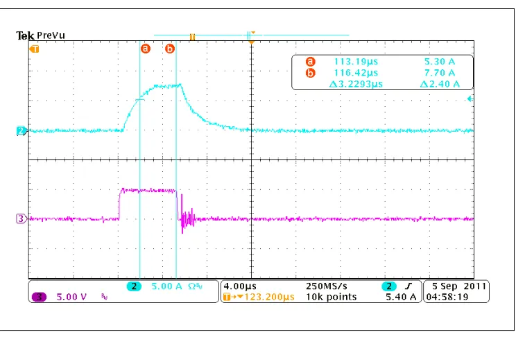
Figure 3.5 below shows output when current threshold is set at 2.7A. Blue waveform
is load current while pink waveform is that of micro-controller output command to
opto-coupler and gate driver. The system makes 3 auto-reclosure attempts and if the fault is still
persistent main switch remains off until micro-controller is reset manually. Figure 3.5 shows
measured time as 52.6uS as against chosen value 50uS because of other instructions
(conditional instructions, incrementing counter) that need to be executed before switch is
turned ON again. It is important to note that time taken by micro-controller can vary upto a
maximum of 2.2uS depending on which instruction the micro-controller is executing when a
26
Figure 3.5 SSCB system operation at 2.7A threshold
27
Figure 3.7 First step, micro-controller and sensor circuitry time (Threshold=2.7A)
Figures 3.6 through figure 3.13 show steps followed by SSCB while tackling a
persistent fault. Figure 3.6 shows first step while tackling a persistent fault. Before fault
occurred, load current was 1A. When fault occurs, current starts to rise and as a result,
current sensor circuitry output (sensor and OPAMP buffer) begins to rise. When feedback to
micro-controller increases beyond programmed threshold, the micro-controller sends OFF
command to opto-coupler and gate driver circuitry. This is seen as pink waveform
(micro-controller output) falling off in figure 3.6. Gate driver and opto-coupler take finite amount of
time to send OFF command to main switch and finally main switch takes some time to turn
OFF and then load current (blue waveform) begins to commutate to freewheeling diode
28
From figure 3.6, total operation time is seen to be 1.48uS which is less than maximum
calculated time 4.042uS. Figure 3.7 shows total operating time of micro-controller and sensor
circuitry as 1.025uS which is less than maximum calculated 3.54uS. This implies that total
time taken by opto-coupler, gate driver and main switch to turn off is 1.48uS-1.025uS=
455nS which is less than maximum calculated amount 502nS.
After micro-controller sends OFF command to opto-coupler and gate driver, it waits
for 50uS (auto-reclosure time) and sends command to turn ON main switch again. Figure 3.8
shows turn ON and subsequent turn OFF which happens since fault is still present.
29
Figure 3.9 Second step, micro-controller and sensor time (Threshold=2.7A)
Since the fault is persistent when micro-controller makes first auto-reclosure attempt,
the system goes through same process as before and eventually micro-controller turns off the
main switch. From figure 3.8, total operation time is seen to be 3.238uS which is less than
maximum calculated time 4.042uS. Total operating time of sensor circuitry and
micro-controller is 2.865uS as shown in figure 3.9 which is less than maximum calculated 3.54uS.
This implies that total time taken by opto-coupler, gate driver and main switch to turn off is
3.238uS-2.865uS= 373nS which is less than maximum calculated 502nS.
30
Figure 3.10 Third step, total time (Threshold=2.7A)
31
Again as fault is still there when micro-controller makes second auto-reclosure
attempt, the system goes through same process as before and eventually micro-controller
turns off the main switch. From figure 3.10, total operation time is seen to be 3.249uS which
is less than maximum calculated time 4.042uS. Total operating time of sensor circuitry and
micro-controller is 2.822uS as shown in figure 3.11 which is less than maximum calculated
3.54uS. This implies that total time taken by opto-coupler, gate driver and main switch to
turn off is 3.249uS-2.822uS= 427nS which is less than maximum calculated 502nS.
After 50uS, micro-controller makes another attempt to check if fault is still there.
32
Figure 3.13 Fourth step, micro-controller and sensor time (Threshold=2.7A)
Finally micro-controller makes third and last auto-reclosure attempt and the system
goes through same process as before and eventually micro-controller turns off the main
switch as fault it persistent. From figure 3.12, total operation time is seen to be 3.195uS
which is less than maximum calculated time 4.042uS. Total operating time of sensor circuitry
and micro-controller is 2.822uS as shown in figure 3.13 which is less than maximum
calculated 3.54uS. This implies that total time taken by opto-coupler, gate driver and main
switch to turn off is 3.195uS-2.822uS= 373nS which is less than maximum calculated 502nS.
Note that time scale on figure 3.13 is 2uS/div which makes pulses look wider than that in
figure 3.12. When the fault is cleared, micro-controller needs to be reset manually in order to
33
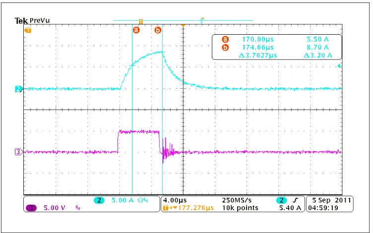
3.3.2 Case 2: Current threshold=5.5A
Figure 3.14 below shows output when current threshold is set at 5.5A. Blue waveform
is load current while pink waveform is that of micro-controller output command to
opto-coupler and gate driver. As in previous case, the system makes 3 auto-reclosure attempts and
if the fault is still persistent main switch remains off until micro-controller is reset manually.
Figure 3.14 shows measured time as 52.6uS as against chosen value 50uS because of other
instructions (conditional instructions, incrementing counter) that need to be executed before
switch is turned ON again. It is important to note that time taken by micro-controller can
vary upto a maximum of 2.2uS depending on which instruction the micro-controller is
executing when a fault occurs.
34
Figure 3.15 First step, total time (Threshold=5.5A)
35
From figure 3.15, total operation time is seen to be 1.179uS which is less than
maximum calculated time 4.042uS. Figure 3.16 shows total operating time of
micro-controller and sensor circuitry as 808nS which is less than maximum calculated 3.54uS. This
implies that total time taken by opto-coupler, gate driver and main switch to turn off is given
by 1.179uS-808nS= 371nS which is less than maximum calculated 502nS.
After micro-controller sends OFF command to opto-coupler and gate driver, it waits
for 50uS (auto-reclosure time) and sends command to turn ON main switch again. Figure
3.17 shows turn ON and subsequent turn OFF which happens since fault is still present.
36
Figure 3.18 Second step, micro-controller and sensor time (Threshold=5.5A)
Since the fault is persistent when micro-controller makes first auto-reclosure attempt,
the system goes through same process as before and eventually micro-controller turns off the
main switch. From figure 3.17, total operation time is seen to be 3.021uS which is less than
maximum calculated time 4.042uS. Total operating time of sensor circuitry and
micro-controller is 2.648uS as shown in figure 3.18 which is less than maximum calculated 3.54uS.
This implies that total time taken by opto-coupler, gate driver and main switch to turn off is
3.021uS-2.648uS= 373nS which is less than maximum calculated 502nS.
37
Figure 3.19 Third step, total time (Threshold=5.5A)
38
Again as fault is still there when micro-controller makes second auto-reclosure
attempt, the system goes through same process as before and eventually micro-controller
turns off the main switch. From figure 3.19, total operation time is seen to be 3.656uS which
is less than maximum calculated time 4.042uS. Total operating time of sensor circuitry and
micro-controller is 3.229uS as shown in figure 3.20 which is less than maximum calculated
3.54uS. This implies that total time taken by opto-coupler, gate driver and main switch to
turn off is 3.656uS-3.229uS= 427nS which is less than maximum calculated 502nS.
39
Figure 3.22 Fourth step, micro-controller and sensor time (Threshold=5.5A)
Finally after 50uS, micro-controller makes third and last auto-reclosure attempt and
the system goes through same process as before and eventually micro-controller turns off the
main switch as fault it persistent. From figure 3.21, total operation time is seen to be 3.763uS
which is less than maximum calculated time 4.042uS. Total operating time of sensor circuitry
and micro-controller is 3.336uS as shown in figure 3.22 which is less than maximum
calculated 3.54uS. This implies that total time taken by opto-coupler, gate driver and main
switch to turn off is 3.763uS-3.336uS= 427nS which is less than maximum calculated 502nS.
When the fault is cleared, micro-controller needs to be reset manually in order to supply the
40
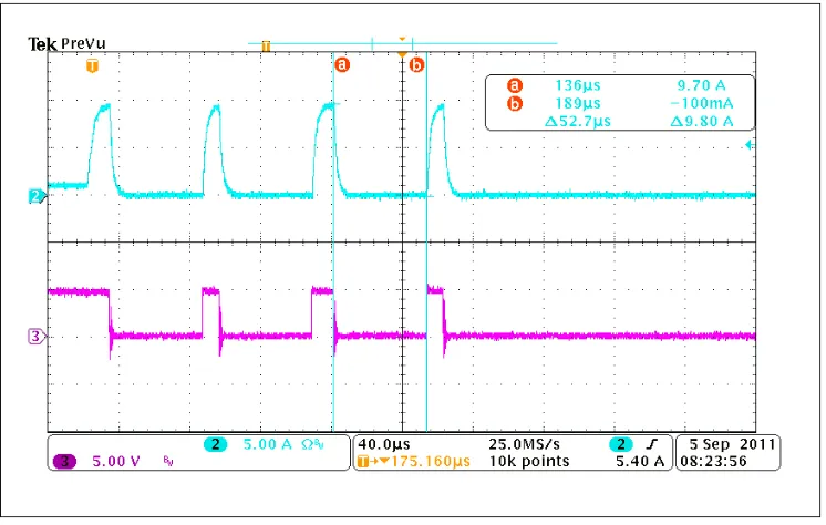
3.3.3 Case 3: Current threshold=8.1A
Figure 3.23 below shows output when current threshold is set at 8.1A. Blue waveform
is load current while pink waveform is that of micro-controller output command to
opto-coupler and gate driver. As in previous case, the system makes 3 auto-reclosure attempts and
if the fault is still persistent main switch remains off until micro-controller is reset manually.
Figure 3.23 shows measured time as 52.7uS as against chosen value 50uS because of other
instructions (conditional instructions, incrementing counter) that need to be executed before
switch is turned ON again. It is important to note that time taken by micro-controller can
vary upto a maximum of 2.2uS depending on which instruction the micro-controller is
executing when a fault occurs.
41
Figure 3.24 First step, total time (Threshold=8.1A)
42
From figure 3.24, total operation time is seen to be 7.66uS which is more than
maximum calculated time 4.042uS. Figure 3.25 shows total operating time of
micro-controller and sensor circuitry as 7.286uS which is more than maximum calculated 3.54uS.
This implies that total time taken by opto-coupler, gate driver and main switch to turn off is
given by 7.66uS-7.286uS= 374nS which is less than maximum calculated 502nS. This means
that SSCB does not meet its predicted operating time due to extra time taken by current
sensor and micro-controller.
After micro-controller sends OFF command to opto-coupler and gate driver, it waits
for 50uS (auto-reclosure time) and sends command to turn ON main switch again.
43
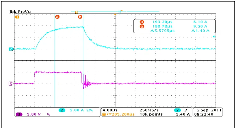
Figure 3.27 Second step, micro-controller and sensor time (Threshold=8.1A)
Since the fault is persistent when micro-controller makes first auto-reclosure attempt,
the system goes through same process as before and eventually micro-controller turns off the
main switch. From figure 3.26, total operation time is seen to be 5.313uS which is more than
maximum calculated time 4.042uS. Total operating time of sensor circuitry and
micro-controller is 4.886uS as shown in figure 3.27 which is more than maximum calculated
3.54uS. This implies that total time taken by opto-coupler, gate driver and main switch to
turn off is 5.313uS-4.886uS= 427nS which is less than maximum calculated 502nS. Again,
SSCB does not meet its predicted operating time due to extra time taken by current sensor
44
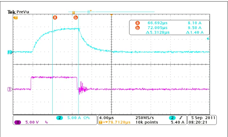
Figure 3.28 Third step, total time (Threshold=8.1A)
45
Figure 3.28 and figure 3.29 show second auto-reclosure attempts made by
micro-controller. Again as fault is still there, the system goes through same process as before and
eventually micro-controller turns off the main switch. From figure 3.28, total operation time
is seen to be 8.46uS which is more than maximum calculated time 4.042uS. Total operating
time of sensor circuitry and micro-controller is 8.14uS as shown in figure 3.20 which is more
than maximum calculated 3.54uS. This implies that total time taken by opto-coupler, gate
driver and main switch to turn off is 8.46uS-8.14uS= 320nS which is less than maximum
calculated 502nS. And once again, SSCB does not meet its predicted operating time due to
extra time taken by current sensor and micro-controller.
46
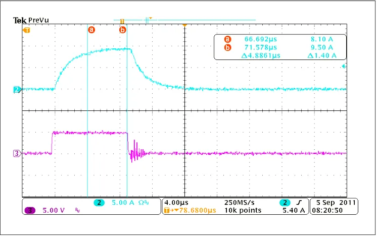
Figure 3.31 Fourth step, micro-controller and sensor time (Threshold=8.1A)
Finally micro-controller makes third and last auto-reclosure attempt and the system
goes through same process as before and eventually micro-controller turns off the main
switch as fault it persistent. From figure 3.30, total operation time is seen to be 5.58uS which
is more than maximum calculated time 4.042uS. Total operating time of sensor circuitry and
micro-controller is 5.26uS as shown in figure 3.31 which is more than maximum calculated
3.54uS. This implies that total time taken by opto-coupler, gate driver and main switch to
turn off is 5.58uS-5.26uS= 320nS which is less than maximum calculated 502nS. When the
fault is cleared, micro-controller keeps main switch open indefinitely till micro-controller is
47
It is clear from results that total operating time is exceeding calculated maximum time
because of extra time taken by current sensor circuitry and micro-controller. As maximum
number of instructions to be executed is same for micro-controller, this extra time must be
being introduced by current sensor circuitry. In order to investigate where this extra delay is
coming from, more analysis is performed on current sensor circuitry operating time in next
chapter.
3.4 Hardware testing results at 400V
48
The final test for a hardware circuit is to test it at conditions for which it was designed
originally. For this purpose, solid state circuit breaker board is interfaced with 400V DC
testbed developed as a part of ongoing research in FREEDM center as shown in figure 3.32.
Input to the system is 208VLL which feeds a 40kVA 3 phase transformer. A DSP is
used to control a 12-pulse thyristor bridge which produces a 400V DC output. LC filter
(7.5mH and 1200uF) is used to filter out ripple present in DC. Total capacity of the system is
12kVA.
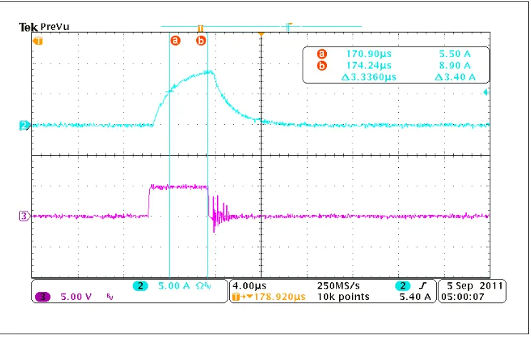
The SSCB hardware is tested at 5.5A threshold with load changing from 85.5ohm to
19.344ohm so that load current is initially 4.68A and could go to 20.68A steady state if not
interrupted. Figure 3.33 below shows output when current threshold is set at 5.5A. Brown
waveform is input voltage while pink waveform is that of load current. Fault is emulated by
changing load resistance. The system makes 3 auto-reclosure attempts and since the fault is
still persistent, main switch remains off until micro-controller is reset manually. Figure 3.33
49
Figure 3.33 SSCB system operation at 5.5A threshold, 400V
50
From figure 3.34, total operation time is seen to be 2.72uS which is less than
maximum calculated time 4.042uS. After micro-controller sends OFF command to
opto-coupler and gate driver, it waits for 50uS (auto-reclosure time) and sends command to turn
ON main switch again. Figure 3.35 shows turn ON and subsequent turn OFF which happens
since fault is still present.
Figure 3.35 Second step, total time at 400V (Threshold=5.5A)
Since the fault is persistent when micro-controller makes first auto-reclosure attempt,
the system goes through same process as before and eventually micro-controller turns off the
51
maximum calculated time 4.042uS. After 50uS, micro-controller makes another attempt to
check if fault is still there.
Figure 3.36 Third step, total time at 400V (Threshold=5.5A)
Again as fault is still there when micro-controller makes second auto-reclosure
attempt, the system goes through same process as before and eventually micro-controller
turns off the main switch. From figure 3.19, total operation time is seen to be 2.08uS which is
52
Figure 3.37 Fourth step, total time (Threshold=5.5A)
Finally after 50uS, micro-controller makes third and last auto-reclosure attempt and
the system goes through same process as before and eventually micro-controller turns off the
main switch as fault it persistent. From figure 3.37, total operation time is seen to be 2.08uS
which is less than maximum calculated time 4.042uS. When the fault is cleared,
micro-controller needs to be reset manually in order to supply the load again.
The results show that the hardware consistently operates as intended within desired
53
CHAPTER 4
Prediction of sensor operation time
Hardware results from previous chapter indicate that operation time was found to be
higher for one of the overcurrent threshold values. Since this phenomenon is threshold
dependent, an investigation needs to be carried out on current sensor operating time. This
chapter focuses on developing a mathematical expression for sensor response time using first
order models of components used in hardware. This expression enables us to calculate
expected sensor operating time for a given system, given current sensor and a given
threshold. A simulation is also performed with models of actual components used for
hardware implementation to verify the result obtained by calculations.
4.1 Mathematical derivation for sensor response time
Let V be the source voltage, L be the total inductance in power circuit and R be total
resistance of power circuit. Time constant of power circuit is give byτs =L/R. Let the
bandwidth of sensor beωBW. Applying KVL to power circuit we get
V = R*i +L* di/dt
Taking Laplace transform,
54
Thus i(s)=
) *
(R s L
s V +
Let i(s)= +
s A L s R B *
+ where values of A and B are to be calculated.
Using partial fraction technique we get
= A
R V
; B= R
L V * −
Thus i(s)=
+ − = + − s s s s R V L s R L s R V τ τ * 1 1 * 1
Taking inverse Laplace transform,
i(t) = R V
* (1- e-t/τ) (4.1)
Now sensor transfer function is given by
BW
s*τ 1
1
+ where BW
BW ω
τ = 1
Therefore output of sensor is product of transfer functions of current and sensor.
BW s s s s s R V s i τ τ τ * 1 1 * * 1 1 ) ( ' + + − = + + − + = BW s s
BW s s
s s R V s i τ τ τ
τ 1 *
1 * * 1 * 1 1 * 1 ) ( '
Again using partial fraction technique, we get
55
Taking inverse Laplace transform,
− + − −
= − −t BW
BW s BW s t BW s s e e R V t
i τ τ
τ τ τ τ τ τ / / ' * ) ( * ) ( 1 )
( (4.2)
Equation 4.1 can be used to find time taken by load current to reach set threshold and
equation 4.2 can be used to calculate sensor response time to reach the same threshold.
4.2 Calculation of sensor response time
In this section, sensor response time is calculated for all three current thresholds used
in 60V testing and is later compared with that obtained with simulation performed in next
section of this chapter. For a given system, source voltage V, inductance in power circuit L
and resistance in power circuit R are fixed. For a given current sensor, ωBW is fixed. To find
response time, first we need to calculate how much time current will take to reach the
threshold using equation 4.1. Then using equation 4.2, we can calculate at what time
response will reach the same value. The difference between the two times is the time taken
by current sensor.
For all cases, V=60V, R=6.45ohm, L=16uH, u R
L
s = =2.48
τ and for sensor τBW is
calculated using u
BW
BW 0.7958
200000 *
2 1
1 = =
=
π ω
τ .
4.2.1 Case 1: Current threshold=2.7A
56
2.7=9.3023*(1- e-t/2.48u)
Solving for t, we get t = t1= 0.85uS
This means that current will take 0.85uS to reach 2.7A threshold if it starts at t=0.
Now putting same values (as used in equation 4.1) in equation 4.2,
2.7=9.3023*(1-1.4725*e-t/2.48u+0.4725*e-t/0.7958u)
Solving for t, we get t = t2= 1.599uS
This means that sensor response will reach 2.7A at t2= 1.599uS.
Therefore, sensor response time = t2- t1 =1.599uS-0.85uS= 0.749uS
4.2.2 Case 2: Current threshold=5.5A
Putting values mentioned in section 4.2 and threshold=5.5A in equation 4.1, we get
5.5=9.3023*(1- e-t/2.48u)
Solving for t, we get t = t1= 2.219uS
This means that current will take 2.219uS to reach 5.5A threshold if it starts at t=0.
Now putting same values (as used in equation 4.1) in equation 4.2,
5.5=9.3023*(1-1.4725*e-t/2.48u+0.4725*e-t/0.7958u)
Solving for t, we get t = t2= 3.124uS
This means that sensor response will reach 5.5A at t2= 3.124uS.
Therefore, sensor response time = t2- t1 =3.124uS-2.219uS= 0.905uS
4.2.3 Case 3: Current threshold=8.1A
Putting values mentioned in section 4.2 and threshold=8.1A in equation 4.1, we get
57
Solving for t, we get t = t1= 5.074uS
This means that current will take 5.074uS to reach 8.1A threshold if it starts at t=0.
Now putting same values (as used in equation 4.1) in equation 4.2,
8.1=9.3023*(1-1.4725*e-t/2.48u+0.4725*e-t/0.7958u)
Solving for t, we get t = t2= 6.03uS
This means that sensor response will reach 8.1A at t2= 6.03uS.
Therefore, sensor response time = t2- t1 =6.03uS-5.074uS= 0.956uS
4.3 Simulation to verify sensor response time
It is seen from calculations above that time taken by sensor is less than 1uS as
mentioned in datasheet. To verify values calculated above, a simulation is performed with
correct values of components and sources used in hardware realization. Current sensor is
modeled as a first order transfer function. Both actual current and current sensor response are
showed on scope captures below to calculate sensor response time. Circuit used in simulation
58
Figure 4.1 Simulation of circuit to measure current sensor response time
Simulation results are also presented below with cursors measuring the sensor
response time. Figure 4.2 shows that for threshold=2.7A, response time is 0.747uS which
closely matches with calculated value 0.749uS. Figure 4.3 shows that for threshold=5.5A,
response time is 0.904uS which closely matches with calculated value 0.905uS. Figure 4.4
59
60
61
62
The equations derived in this chapter provide a tool for prediction of sensor operating
time with restrictions explained at the end of next chapter where conclusions are drawn by
63
CHAPTER 5
SPICE simulations of 7.5kV DC system
In this chapter, simulations are performed for 7.5kV DC system using SPICE models
of different devices. The purpose of these simulations is to evaluate and compare the
performance of a solid state circuit breaker (SSCB) using actual models of devices. Knowing
trade-offs between different options helps circuit designer to choose appropriate device for
his application. The simulation is first performed with Si-IGBT and later is repeated with
SiC-MOSFET to compare the performance.
5.1 System description
Figure 5.1 shows the system on which simulations are carried using different devices.
A 1MW diode rectifier bridge is used as a source for the SSCB. For SPICE simulations,
6.5kV Si-diode model is used. AC source of 5.56kVrms L-L is used as input to rectifier.
Input inductors are chosen such that voltage drop across them is less than 5% of input
voltage. The DC link voltage was chosen to be 7.5kV and a 5000µF DC link capacitor was
selected. The load was selected such that it absorbs 1MW power at rated DC link voltage of
7.5kV.
64
The topologies for MVAC FID are elaborated in [11] and [12]. The topology
mentioned in [11] is chosen because then we do not need to use series diodes. For MVDC
FID, current flow is going to be unidirectional, so instead of 6 devices we need to have only
three 6.5kV IGBT connected in series. Three switches are used in order to have redundancy.
To simulate a fault, the load on system is increased by 100%. After a period if 2uS (time
taken to sense the fault and take corrective action), all three switches open simultaneously to
break the fault current. The circuit diagram is shown in figure 5.1.
65
5.2 Simulation results with Si-IGBT
The circuit shown in figure 5.1 is simulated to get results shown in figure 5.2 which
shows load voltage as red waveform and three IGBT voltages as green, violet and yellow
waveforms. It is seen that load voltage falls quickly once IGBTs begin to open and in steady
state they share DC bus voltage more or less equally. Figure 5.3 shows a zoomed in view of
the figure 5.1 at the turn off instant with waveform for current (sky blue) added.
66
Figure 5.3 Zoomed in results with Si-IGBT
When the fault occurs at t=49.999mS (load changes to twice of its previous value),
load current shoots to twice of its steady state value. After a delay of 2uS (operation time of
control circuitry), IGBTs begin to turn off at 50.001mS and load current begins to fall. In
about 13uS, load current reduces to 220mA and corresponding load voltage is 13V. All
IGBTs share the voltage equally for the initial period seen in the above waveform. About
400uS after fault event, voltages across IGBTs begin to deviate from each other as shown in
figure 5.4. In steady state, voltage across IGBT 3 is higher than other two by 21V as shown
67
Figure 5.4 VCE voltage variation with Si-IGBT
68
Now, some time delay is added into the circuit. The reason we want to examine this
case is because in practice no two components are exactly the same and thus in a practical
circuit it is possible that gate signals to IGBT may not be perfectly synchronized. Let IGBT 2
begin to turn off 50nS later than IGBT 1 and IGBT 3 begins to turn off 50nS earlier than
IGBT 1. The waveforms obtained are shown in figure 5.6.
Figure 5.6 Zoomed in results with Si-IGBT (50nS delay)
We see that there is not much difference than the ideal case in which all IGBTs begin
to turn off at the same time. Figure 5.7 shows the waveforms in more details when the IGBTs
69
difference in voltage across each IGBT since they are commanded to open at different times.
However in steady state voltage shared by them is same as in the ideal case (when all of them
open at the same time) as shown in figure 5.8.
70
Figure 5.8 Steady state VCE with Si-IGBT (50nS delay)
To simulate even greater time difference, let IGBT 2 begin to turn off 150nS later than
IGBT 1 and IGBT 3 begins to turn off 150nS earlier than IGBT 1. The waveforms obtained
71
Figure 5.9 Zoomed in results with Si-IGBT (150nS delay)
We see that there is not much difference than the ideal case in which all IGBTs begin
to turn off at the same time. Figure 5.10 shows the waveforms in more details when the
IGBTs are in the processes of opening. In the waveforms we see that initially there is
difference in voltage across each IGBT since they are commanded to open at different times.
However in steady state voltage shared by them is same as in the ideal case (when all of them
72
Figure 5.10 VCE voltage variation with Si-IGBT (150nS delay)
73
5.3 Simulation results with SiC MOSFET
The circuit shown in figure 5.1 is modified by replacing IGBT with SiC-MOSFET
and simulations are repeated. Simulation results are shown in figure 5.12 which shows load
voltage as red waveform, SiC-MOSFET voltages as green, violet and yellow waveforms. It is
seen that load voltage falls quickly once SiC-MOSFETs begin to open and in steady state
they share DC bus voltage equally. Figure 5.13 shows a zoomed in view of figure 5.12 at the
turn off instant.
74
Figure 5.13 Zoomed in results with SiC-MOSFET
When the fault occurs at t=49.999mS (load changes to twice its previous value), load
current tries to shoots to twice of its steady state value. After a delay of 2uS (operation time
of control circuitry), MOSFET begin to turn off at 50.001mS and load current begins to fall.
It is observed that load current drops to zero in less than 1uS and SiC-MOSFET voltage
drops to 15V in less than 5uS. Current is inhibited 10 times faster than Si-IGBT but at the
cost of higher conduction loss. Notably, voltage across each SiC-MOSFET is the same
75
Figure 5.14 VDS voltages variation with SiC-MOSFET
76
To simulate asynchronous operation of circuit, let MOSFET 2 begin to turn off 50nS
later than MOSFET 1 and MOSFET 3 begins to turn off 50nS earlier than MOSFET 1. The
waveforms obtained are shown in figure 5.16.
Figure 5.16 Zoomed in results with SiC-MOSFET (50nS delay)
In the waveforms below it is seen that initially there is difference in voltage across
each MOSFET since they are commanded to open at different times. However in steady state
voltage shared by them is same as in the ideal case (when all of them open at the same time)
77
Figure 5.17 VDS voltage variation with SiC-MOSFET (50nS delay)
![Figure 1.1 FREEDM system single line diagram [3]](https://thumb-us.123doks.com/thumbv2/123dok_us/1453772.1178111/15.595.123.491.155.457/figure-freedm-system-single-line-diagram.webp)