University of Windsor University of Windsor
Scholarship at UWindsor
Scholarship at UWindsor
Electronic Theses and Dissertations Theses, Dissertations, and Major Papers
5-16-2018
Development and Integration of Stretchable Electronic
Development and Integration of Stretchable Electronic
Components into Light-Emitting Devices.pdf
Components into Light-Emitting Devices.pdf
Yiting ChenUniversity of Windsor
Follow this and additional works at: https://scholar.uwindsor.ca/etd
Recommended Citation Recommended Citation
Chen, Yiting, "Development and Integration of Stretchable Electronic Components into Light-Emitting Devices.pdf" (2018). Electronic Theses and Dissertations. 7469.
https://scholar.uwindsor.ca/etd/7469
This online database contains the full-text of PhD dissertations and Masters’ theses of University of Windsor students from 1954 forward. These documents are made available for personal study and research purposes only, in accordance with the Canadian Copyright Act and the Creative Commons license—CC BY-NC-ND (Attribution, Non-Commercial, No Derivative Works). Under this license, works must always be attributed to the copyright holder (original author), cannot be used for any commercial purposes, and may not be altered. Any other use would require the permission of the copyright holder. Students may inquire about withdrawing their dissertation and/or thesis from this database. For additional inquiries, please contact the repository administrator via email
Development and Integration of Stretchable Electronic Components into Light-Emitting Devices
By
Yiting Chen
A Dissertation
Submitted to the Faculty of Graduate Studies
through the Department of Chemistry and Biochemistry
in Partial Fulfillment of the Requirements for
the Degree of Doctor of Philosophy
at the University of Windsor
Windsor, Ontario, Canada
2018
Development and Integration of Stretchable Electronic Components
into Light-Emitting Devices
by
Yiting Chen
APPROVED BY:
_____________________________ J. Yang, External Examiner
Western University
_____________________________ X. Nie
Materials and Mechanical Engineering
_____________________________ J.R. Green
Department of Chemistry and Biochemistry
_____________________________ J. Rawson
Department of Chemistry and Biochemistry
_____________________________ T. Carmichael, Advisor
Department of Chemistry and Biochemistry
iii
Declaration of Co-Authorship / Previous Publications
I. Co-Authorship Declaration
I hereby declare that this thesis incorporates material that is result of joint
research, as follows: This thesis incorporates the outcome of the research undertaken in
Professor Tricia Carmichael’s research group. In all cases, the key ideas, primary
contributions, experimental designs, data analysis, interpretation, and writing were
performed by the author. Chapter 2 and 3 of the thesis was co-authored with R. Stephen
Carmichael under the supervision of Professor Tricia Carmichael. R. Stephen Carmichael
contributed to providing feedback on experimental designs in Chapter 2 and 3 as well as
assisting data analysis of light-emitting devices and acquisition of photograph in Chapter
2. Chapter 4 contains joint research with Danny Mansour, R. Stephen Carmichael under
the supervision of Professor Tricia Carmichael and is the outcome of a collaboration with
Dr. John Trant, Dr. Elizabeth R. Gillies of University of Western. Danny Mansour
contributed to conducting the optoelectronic tests for LEECs fabricated from pristine
iridium complex. R. Stephen Carmichael assisted data analysis of light-emitting devices.
Dr. John Trant and Dr. Elizabeth R. Gillies synthesized the RgP graft copolymer. Chapter
5 of the thesis was co-authored with Yunyun Wu and Sara Mechael under the supervision
of Professor Tricia Carmichael. Both Yunyun Wu and Sara Mechael contributed to
editing of the manuscript. Sara Mechael also contributed to designing the Figure 3 in
iv I am aware of the University of Windsor Senate Policy on Authorship and I
certify that I have properly acknowledged the contribution of other researchers to my
dissertation and have obtained written permission from each of the co-author(s) to
include the above material(s) in my dissertation. I certify that, with the above
qualification, this thesis, and the research to which it refers, is the product of my own
v
II. Declaration of Previous Publication
This thesis includes 4 original papers that will be published/submitted for
publication in peer reviewed journals, as follows:
Dissertation
Chapter Publication title/full citation Publication status
Chapter 2 Yiting Chen, R. Stephen Carmichael, Tricia
Breen Carmichael, “Patterned and Compliant
Transparent Conductive Electrodes Based on Silver Nanowires”
In preparation
Chapter 3 Yiting Chen, R. Stephen Carmichael, Tricia
Breen Carmichael, “Stretchable and Durable
AgNW Composites on Transparent Butyl Rubber”
In preparation
Chapter 4 Yiting Chen, Danny Mansour, R. Stephen
Carmichael, John Trant, Elizabeth R. Gillies,
and Tricia Breen Carmichael, “Stretchable
Light-Emitting Electrochemical Cells Incorporating Butyl Rubber-Poly(ethylene oxide) Graft Copolymers”
In preparation
Chapter 5 Yiting Chen, Yunyun Wu, Sara Mechael, Tricia
Breen Carmichael, “Exploiting the Formation of
Nanocracks in Solution-Deposited Gold Films on PDMS for Stretchable Electronics”
In preparation
I certify that I have obtained a written permission from the copyright owner(s) to
include the above published material(s) in my thesis. I certify that the above material
describes work completed during my registration as a graduate student at the University
vi
III. General
I declare that, to the best of my knowledge, my thesis does not infringe upon
anyone’s copyright nor violate any proprietary rights and that any ideas, techniques,
quotations, or any other material from the work of other people included in my thesis,
published or otherwise, are fully acknowledged in accordance with the standard
referencing practices. Furthermore, to the extent that I have included copyrighted
material that surpasses the bounds of fair dealing within the meaning of the Canada
Copyright Act, I certify that I have obtained a written permission from the copyright
owner(s) to include such material(s) in my thesis.
I declare that this is a true copy of my thesis, including any final revisions, as
approved by my thesis committee and the Graduate Studies office, and that this thesis has
vii
Abstract
Flexible and stretchable electronics are the new format of electronics that remain
functional with mechanical bending, twisting, and stretching. These new kinds of devices
are expected to open up new opportunities and uses by reforming the way we interact
with electronics and fundamentally change our life. To reach these goals, we must move
beyond conventional hard, inorganic materials such as glass and silicon and find ways to
incorporate electrical function into soft materials that are flexible or even stretchable.
This thesis focuses on the development of compliant electronic components including
transparent conductive electrodes, light-emitting materials, and metallic electrodes, and
their integration into soft light-emitting devices.
Chapter 2 reports a new and simple method using shadow masks to produce
flexible and stretchable patterned silver nanowire (AgNW) coatings. We easily obtain a
variety of geometries and resolutions of the patterns using different shadow masks.
These coatings are highly conductive and transparent and exhibit high flexibility,
stretchability, and mechanical robustness. We demonstrate their use as electrodes in
light-emitting electrochemical cells (LEECs) and show that these devices function during
bending.
However, due to the high permeability of PDMS substrate, water and air in
ambient condition easily penetrate through the substrate and corrode AgNW network to
form less conductive particles or rods, making it not suitable for long-term stable
applications. To solve this challenge, Chapter 3 reported the fabrication of a chemical
viii a new airtight material—transparent butyl rubber. The resulting coatings very well
maintain their optical, electrical, and mechanical properties when exposing to extremely
harsh conditions such as underwater or acidic vapor.
Chapter 4 investigates a feasible method to fabricate a stretchable light-emitting
material with an improved optical performance by mixing an ionic transition metal
complex with an elastic graft copolymer and an ionic conductor. The graft copolymer not
only provides the stretchability by its elastic backbone but also acts as ion hosting
materials due to its ion trapping side chains. We demonstrate that devices made from this
material emit bright yellow light and keep emitting light under repetitive strain cycles.
Chapter 5 describes a new, simple, low-cost solution-based scalable method to
produce patterned gold film with microcontact printing on elastomeric
polydimethylsiloxane (PDMS). This solution-based method enables the metal deposition
on not only flat surfaces but also any other irregular shapes. Additionally, the patterning
method is also compatible with uneven surface due to the high comfortability of PDMS.
Unlike traditional physical vapor deposited gold films that experience electrical failure at
ix
Dedication
x
Acknowledgements
First and the most, I would like to thank my parents, Jian Chen and Cuiping Lu
for their moral support in all my decisions and pursuits. I cannot become the person who
I am now without their love, encouragement, and guidance. When I go through any rough
situations, no matter the research obstacles or homesick, they are always there willing to
listen to me and relieve my stress. I also would like to thank my boyfriend, Hongjun Luo,
for releasing my stress anytime I need.
I would like to thank my advisor, Prof. Tricia Carmichael, for offering me the
chance to join her research group. I cannot embark on my wonderful journey of graduate
study without her help. I also need to thank her for her patient guidance, numerous
encouragement, and unflagging support for the past, nearly six, years. Prof. Carmichael’s
passion for research, rigorous work attitude, and the constant quest for excellence have
had a great influence on me now and in the future. Additionally, she not only trained my
skills on designing and conducting a research project but also taught me so much on how
to write scientifically in English and how to present results in an effective way. All these
experiences will be the wealth of my whole life.
I would also like to thank Steve Carmichael for the work to improve my oral
communication skills, the technical discussions to make me think out of the box, the
willingness to share his life experiences with me, and the selfless care of me over the past
few years. I cannot enjoy my experience in Canada so much without his delicious food in
xi I cannot have such an enjoyable time in the laboratory without my colleagues who
have gone through all the happy and sad moments with me in the last six years and I
would not be who I am today without your help. I would like to thank Dr. Akhil Vohra
for training me on all the instruments in the lab when I first started, patient guiding me
through working and life problems, and your continued friendship and support. I would
like to thank Dr. Heather Filiatrault for helping me solve the technical problems, no
matter before or after graduation as well as sharing so many funny moments with me. I
can never forget “DaPiGu” and your bright smile. I would like to thank Yunyun Wu for
being a wonderful friend who works with me, discusses the experimental results with me,
and talks Chinese with me. I would like to thank Sara Mechael for being so nice to
correct all my outlines, inspiring me, taking me to eat delicious food, sharing stories with
me, and I will never forget the beautiful time we have together. I would like to thank
Kory Schlingman for always being so helpful, no matter with laboratory work or life. I
cannot count how many times I have been encouraged and comforted by you. I will
cherish our friendship for life. I would like to thank Brittany Ives for sharing her amazing
experiences over various fields which broads my thoughts. I would like to thank all the
undergraduate students that I have worked with and allowed me to mentor. I have learned
a lot about research and teaching through those experiences. I would like to especially
thank the undergraduate students that contributed to the projects presented in this
dissertation: Danny Mansour and Dominique Leckie. I could not have achieved what I
did without your countless hours of sample preparation and assistance in device testing. I
xii to thank all my friends in the department who created all my best memories in the last
few years.
I would like to thank all the support staffs who have helped me in countless
situations in Chemistry and Biochemistry Department. Thank you to Marlene Bezaire,
Catherine Wilson, and Elizabeth Kickham for the sincere help and support. Thank you to
Joe Lichaa for being dedicated to fixing our instruments and my computer. Thank you to
Sharon Leckie at GLIER for SEM and EDX analysis. Thank you to the staff at Surface
Science Western and the Nanofab at the University of Western Ontario (Dr. Mark
Biesinger, Dr. Todd Simpson, and Tim Goldhawk) for SEM and XPS analysis and the
training on photolithography.
Finally, I would like to thank my committee members: Prof. James Green, Prof.
Jeremy Rawson, Prof. Xueyuan Nie for their feedback at my committee meetings and for
the guidance over the course of my graduate study. I would also like to thank Dr. Jun
Yang for agreeing to be my external examiner. I appreciate all the critiques and
xiii
Table of Contents
Declaration of Co-Authorship / Previous Publications ... iii
Abstract ... vii
Dedication ... ix
Acknowledgements ...x
List of Tables ... xviii
List of Schemes ... xix
List of Figures ...xx
List of Abbreviations / Symbols ... xxxi
1. Chapter 1 ...1
Introduction ...1
1.1. Compliant Electronics ...2
1.2. EL Devices ...2
1.2.1. ACEL Devices ...4
1.2.2. Light Emitting Electrochemical Cells (LEECs) ...4
1.3. Strategies to Incorporate Compliance in Transparent Conductive Electrode (TCE)10 1.3.1. Strategies to Prepare Flexible AgNW-TCEs ...13
1.3.2. Strategies to Prepare Stretchable AgNW-TCEs ...15
1.3.3. Strategies to Prepare Patterned AgNW-TCEs ...16
1.3.4. Challenge of AgNW-TCEs: Degradation of AgNWs ...17
1.4. Strategies to Incorporate Compliance into Emissive Materials ...19
1.5. Strategies to Incorporate Stretchability to Metallic Electrode ...22
xiv
1.5.2. Morphology-Induced Cracking ...26
1.5.3. Deposition of Thin Metal Films Using Electroless Deposition (ELD) ...27
1.6. Dissertation Objectives ...31
1.6.1. Fabrication of Patterned and Durable AgNW Composites on Elastomer ...32
1.6.2. Development of Elastomeric Emissive Materials for Light-Emitting Devices 32 1.6.3. Fabrication of Stretchable Gold Films on PDMS Substrate ...33
1.7. References ...34
2. Chapter 2 ...41
Patterned and Compliant Transparent Conductive Electrode Based on Silver Nanowires41 2.1. Introduction ...42
2.2. Results and Discussion ...47
2.2.1. Fabrication of Patterned AgNW/Polymer Coatings ...47
2.2.2. Pattern Dimensions and Resolution ...50
2.2.3. Morphology of Patterned AgNW/Polymer Coatings ...51
2.2.4. Topography of Patterned AgNW/Polymer Coatings ...53
2.2.5. Electrical and Transmittance Properties of AgNW/Polymer Coatings ...55
2.2.6. Flexibility and Stretchability of Patterned AgNW/Polymer Coatings ...58
2.2.7. Flexible ACEL Devices with Patterned AgNW/OA TCEs ...61
2.3. Conclusions ...63
2.4. Experimental ...64
2.5. References ...67
2.6. Supporting Information ...70
xv
Stretchable and Durable AgNW Composites on Transparent Butyl Rubber ...75
3.1. Introduction: ...76
3.2. Results and Discussion ...79
3.2.1. Fabrication of stretchable AgNW/CF coatings ...79
3.2.2. Surface Morphology of T-IIR/[AgNW]n and PDMS/[AgNW]n Composites ...81
3.2.3. Electrical and Transmittance Properties of T-IIR/[AgNW]n and PDMS/[AgNW]n Composites ...84
3.2.4. Stretchability of T-IIR/[AgNW]n and PDMS/[AgNW]n Composites ...86
3.2.5. T-IIR as a Gas-Diffusion Barrier for AgNW/CF Coatings ...89
3.2.6. Durability of T-IIR/[AgNW]1.0 and PDMS/[AgNW]1.0 Composites ...94
3.3. Conclusions ...95
3.4. Experimental ...96
3.5. References ...99
3.6. Supporting Information ...103
4. Chapter 4 ...108
Stretchable Light-Emitting Electrochemical Cells Incorporating Butyl Rubber-Poly(Ethylene Oxide) Graft Copolymers ...108
4.1. Introduction ...109
4.2. Results and Discussion ...114
4.2.1. RgP/LiCF3SO3/Ir Emissive Films ...116
4.2.2. LEECs Incorporating RgP/LiCF3SO3/Ir Emissive Films ...120
xvi
4.3. Conclusions ...127
4.4. Experimental ...128
4.5. References ...130
4.6. Supporting Information ...133
5. Chapter 5 ...136
Exploiting the Formation of Nanocracks in Solution-Deposited Gold Films on PDMS for Stretchable Electronics...136
5.1. Introduction ...137
5.2. Results and Discussion ...140
5.2.1. Fabrication of ENIG films on PDMS substrate ...140
5.2.2. Resolution of Patterned ENIG Films ...144
5.2.3. Optimization of ENIG Deposition Parameters ...145
5.2.4. Stretchability of ENIG Films on PDMS ...148
5.2.5. Crystallographic Analysis of ENIG20 and EBAu Films ...150
5.2.6. ENIG20 as Stretchable Interconnects and Electrodes ...152
5.3. Conclusions ...155
5.4. Experimental ...156
5.5. References ...158
5.6. Supporting Information ...162
6. Chapter 6 ...171
Conclusions and Outlook ...171
6.1. Conclusions ...172
xvii
6.2.1. Patterned, Compliant, and Durable AgNW Network as TCEs...176
6.2.2. Elastomeric Matrices in LEECs ...177
6.2.3. Stretchable Metal Films ...177
Appendices ...178
Copyright Permission ...179
xviii
List of Tables
Table S2.1. Electrical and optical properties of patterned AgNW/OA and AgNW/CF
lines on PDMS substrate. ... 73
Table 3.1. Summary of electrical and optical properties of T-IIR/[AgNW]n and
PDMS/[AgNW]n composites. ... 85
Table 3.2. Summary of electrical and optical properties of T-IIR/[AgNW]1.0 and
PDMS/[AgNW]1.0 composites before and after exposure to deleterious environments. 92
Table S3.1. Summary of root-mean-square roughness (RRMS) values and peak-to-valley
distances of T-IIR/[AgNW]n and PDMS/[AgNW]n composites. ... 105
Table 4.1. Summary of figures of merit for LEECs fabricated from RgP/LiF3CSO3/Ir
composites on ITO/glass operated at 6 V DC in inert conditions ... 122
Table S4.1. Summary of figures of merit for LEECs fabricated from RgP34/LiCF3SO3/Ir
composite and RgP69/LiCF3SO3/Ir composite on Au/PDMS operated at 6 V DC in inert
xix
List of Schemes
Scheme 2.1. Process used to fabricate patterned AgNW/OA and AgNW/CF coatings on
PDMS substrates. ... 48
Scheme 3.1. Process used to fabricate AgNW/CF coatings on T-IIR or PDMS substrate.
... 81
Scheme 5.1. (a) Illustrated process of patterning ENIG wires on PDMS substrate. (b)
xx
List of Figures
Figure 1.1. (a) Structure of a typical OLED that contains eight layers of active materials.
(b) Structure of a typical ACEL device and LEEC. Adapted with permission from
reference 11. ... 3
Figure 1.2. Illustration of potential profile and electronic along with ionic charge
distribution in a LEEC during steady-state operation for the (a) ED model and (b) ECD
model. Adapted with permission from reference 11. ... 6
Figure 1.3. (a) Materials used in the first PLEC: conjugated polymer of MEH-PPV, ionic
conductors of PEO and lithium trifluoromethanesulfonate salt. (b) The first
[Ru(vbpy)3](PF6)2 RuII-iTMC used for LEECs. (c) Structure of [Ir(bpy)3]+ (bpy =
bipyridine), a sample of the largest class of IrIII-iTMCs used in LEECs. Adapted with
permission from reference 11. ... 8
Figure 1.4. (a) SEM image of AgNW network. Scale bar = 1 m (b) Change in resistance
as a function of thermal annealing temperature. The concentration of AgNW dispersion is
0.75 mg/mL and the deposited density is 105 mg/m2. Adapted with permission from
reference 62. ... 13
Figure 1.5. (a) Cross-sectional SEM image of AgNWs protrusion from the surface of a
substrate. (b) AFM profile measurement of a AgNW film on a silicon wafer. (c)
Cross-sectional SEM image of AgNW-OA coating on a glass substrate. (d) Top view SEM
image of a AgNW-OA coating surface. Adapted with permission from reference 78 (a)
xxi
Figure 1.6. (a) SEM and (b) TEM images of corroded AgNW network after storing in
ambient conditions for 30 days. (c) Illustration of core-shell structure that protects AgNW
from interacting with corrosive environments. The green shell represents the gold shell
and red core represents the silver core. (d) Schematic structure of the graphene barrier on
top of AgNW network on PET substrate. Adapted with permission from reference 92 (a),
90 (b), 95 (c), and 101 (d). ... 18
Figure 1.7. Examples of intrinsically stretchable light-emitting devices: (a) stretchable
PLEC, (b) stretchable iTMC-LEEC, and (c) stretchable ACEL devices. Adapted with
permission from reference 80 (a), 104 (b), and 105 (c). ... 21
Figure 1.8. Illustrative scheme of (a) fracture of freestanding metal film and (b) the local
elongation in the film suppressed by the substrate when the film well adheres to a
substrate. (c) Optical micrograph of the gold film on PDMS substrate at 20% strain. (d)
Normalized change in resistance as a function of applied tensile strain. Adapted with
permission from reference 111 (a, b) and 123(c) and 114(d). ... 23
Figure 1.9. SEM images of (a) stretchable wavy ribbons, (b) popup structure, and (c)
coplanar serpentine designs. Adapted with permission from reference 117 (a), 118 (b) and
119 (c). ... 25
Figure 1.10. (a) SEM micrograph of gold film on nanopatterned pyramids with 30° tilt.
(b) SEM of gold film on random features at 0% strain. (c) Optical micrograph of gold
film on random features at 60% strain. Adapted with permission from reference 121 (a),
xxii
Figure 1. 11. Schematic illustration of ELD process. After deposition of the catalyst, the
substance is first immersed into a typical Pd/Sn colloidal catalyst bath. In the following
accelerator step, the Sn shell is etched away, exposing the inner Pd core. In the last ELD
bath, the metallic ions are deposited on a catalyzed surface. The initial layer of metal
further initiates the metal deposition with the presence of reducing agent and eventually
results in a continuous metal thin film. ... 29
Figure 1.12. Schematic illustration of patterning copper films using (a) CP and (b)
MACP process. Adapted with permission from reference 132 (a) and 136 (b). ... 31
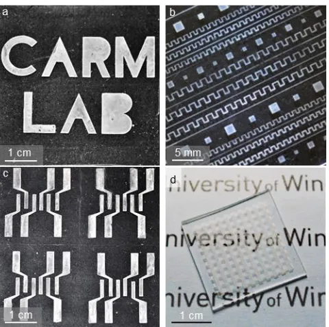
Figure 2.1. (a) Optical micrograph of letters with various curvatures. (b) Optical
micrograph of square and square wave patterns. (c) Optical micrograph of four sets of
electrodes. Each set consisted of six polygonal chains. (d) Photograph of a patterned grid.
Overall sample dimensions are (a-c) 5 cm x 5 cm and (d) 2.5 cm x 2.5 cm. ... 51
Figure 2.2. SEM images of patterned AgNW/OA lines with widths of (a) 50 m and (b)
300 m on PDMS substrate. Higher magnification of AgNW networks at the (c) centre
and (d) edge of 2000-m-wide AgNW/OA lines. ... 53
Figure 2.3. AFM height images (Z scale = 150 nm) with RRMS measurements and
corresponding profile measurements of patterned (a, d) AgNW/OA and (b, e) AgNW/CF
lines (20 mm x 2 mm) on PDMS fabricated using a 2 mg/mL AgNW dispersion. AFM
height image (Z scale = 350 nm) with RRMS measurements and corresponding profile
measurement of (c, f) an unpatterned AgNW network fabricated by drop-casting a 2
xxiii
Figure 2.4. (a) Photograph of patterned AgNW/OA lines on PDMS substrate used for Rs
and transmittance measurements. Transmittance spectra of patterned (b) AgNW/OA and
(c) AgNW/CF lines on PDMS substrates with corresponding Rs. Dotted line shows the
transmittance spectrum of the (b) PDMS/OA and (c) PDMS/CF composite without
AgNWs. ... 57
Figure 2.5. (a) Photograph of patterned AgNW/OA lines on PDMS substrate with
various line widths and lengths of 2 cm. Rs as a function of linewidth for patterned (b)
AgNW/OA and (c) AgNW/CF lines made from a 2 mg/mL AgNW dispersion. ... 58
Figure 2.6. (a) Change in resistance of 20 mm x 2 mm AgNW/OA lines on PDMS
substrate as a function of bending strain. (b) Change in resistance of 20 mm x 2 mm
AgNW/OA lines on PDMS versus the number of 15% bending strain cycles. (c) Change
in resistance of 20 mm x 2 mm AgNW/CF lines on PDMS as a function of stretching
strain. (d) Change in resistance of 20 mm x 2 mm AgNW/CF lines on PDMS versus the
number of 30% stretching strain cycles. The concentration of the AgNW dispersion used
in all cases was 2 mg/mL. ... 60
Figure 2.7. (a) Diagram of the flexible ACEL device structure. (b) Photographs of
flexible ACEL devices fabricated with a patterned AgNW/OA (2 mg/mL) coating on
PDMS as the TCE, bent to various strains. (c) Temporal evolution of radiance of a typical
device operated under 150 V AC in ambient conditions before and after being subjected
to repetitive 20% bending strain cycles. ... 62
xxiv
Figure S2.1. Photographs of OA coating on PDMS substrate (a) at 0% strain and (b)
fractured at 20% strain. (c) Cross-sectional optical micrograph of OA coating on PDMS
substrate after fracture at 20% strain. The OA coating (in the red frame) remains adhered
to the PDMS substrate after fracture. Photographs of CF coating on PDMS substrate (d)
at 0% strain and (e) fractured at 106% strain. (f) Cross-sectional optical micrograph of
CF coating on PDMS substrate after fracture at 106% strain. The CF coating (in the red
frame) remains adhered to the PDMS substrate after fracture. ... 70
Figure S2.2. Photographs of (a) AgNW/OA coating on PDMS substrate and (b) PDMS
template after the transferring process. (c) Optical micrograph of PDMS template after
the transferring process, showing that no AgNW residue was observed. ... 71
Figure S2.3. Photographs of AgNW/OA coatings on PDMS substrate (a) before and (b)
after 10 peel-off tests. (c) Optical micrograph of the tape after 10 peel-off tests of
AgNW/OA coating on PDMS substrate. Photographs of AgNW/CF coatings on PDMS
substrate (d) before and (e) after 10 peel-off tests. (f) Optical micrograph of the tape after
10 peel-off tests of AgNW/CF coating on PDMS substrate. ... 71
Figure S2.4. Photographs of patterned AgNW/CF coatings on PDMS substrates. ... 72
Figure S2.5. Cross-sectional SEM image of a freeze-fractured (a) AgNW/OA and (b)
AgNW/CF coating on silicon wafer fabricated using a 2 mg/mL AgNW dispersion. (c)
SEM image of the AgNW/CF coating surface on silicon wafer. ... 72
Figure S2.6. AFM height image with RRMS measurement and corresponding profile
xxv substrate over a scanning area of 100 m x 100 m (z scale = 150 nm). The
concentration of the AgNW dispersion used was 2 mg/mL. ... 73
Figure S2.7. Delaminated copper tape (in the red frame) from the emissive layer of a
flexible ACEL device after 60 cycles of 20% bending strain. ... 74
Figure 3.1. Top view SEM images (scale = 5 m) of (a) T-IIR/[AgNW]0.5, (b)
T-IIR/[AgNW]0.7, (c) T-IIR/[AgNW]1.0, and (d) T-IIR/[AgNW]2.0 composites. AFM height
images (scale = 2 m, z-scale = 250 nm) with RRMS measurements and corresponding
profile measurements of (e, i) T-IIR/[AgNW]0.5, (f, j) T-IIR/[AgNW]0.7, (g, k)
T-IIR/[AgNW]1.0, and (h, l) T-IIR/[AgNW]2.0 composites. ... 82
Figure 3.2. Transmittance spectra of (a) T-IIR/[AgNW]n and (b) PDMS/[AgNW]n
composites. Dotted line represents the transmittance spectrum of (a) T-IIR substrate and
(b) PDMS substrate. ... 85
Figure 3.3. Resistance as a function of tensile strain of (a) T-IIR/[AgNW]n and (b)
PDMS/[AgNW]n composites, where n = 0.5 mg/mL (black lines), 0.7 mg/mL (blue lines),
1.0 mg/mL (red lines), and 2.0 mg/mL (green lines). ... 87
Figure 3.4. SEM images (scale = 1 m) of T-IIR/[AgNW]1.0 composites after (a)
exposure to 45 °C/ 95% RH for 30 days, (b) immersed in water for 7 days, and (c)
exposure to nitric acid vapor for 24 hours. SEM images of PDMS/[AgNW]1.0 composites
after (d) exposure to 45 °C/ 95% RH for 30 days, (e) immersed in water for 7 days, and
xxvi
Figure 3.5. Resistance of (a) T-IIR/[AgNW]1.0 and (b) PDMS/[AgNW]1.0 composites as
a function of tensile strain before (black lines) and after exposure to 45 °C/ 95% RH for
30 days (green lines) and immersion in water for 7 days (red lines). ... 93
Figure 3.6. (a) Resistance of T-IIR/[AgNW]1.0/T-IIR (black line) and
PDMS/[AgNW]1.0/PDMS (red line) structures as a function of the time and 15%
strain/relaxation cycles after exposure to 45 °C/ 95% RH for 30 days. (b) Resistance of
T-IIR/[AgNW]1.0/T-IIR/ (black line) and PDMS/[AgNW]1.0 /PDMS (red line) structures
as a function of the time and 15% strain/relaxation cycles after immersion in water at
room temperature for 7 days. ... 95
Figure S3.1. Photograph of T-IIR/[AgNW]1.0 composites (a) before and (b) after
adhesion test with a Scotch tape. (c) Optical micrograph (scale = 200 m) of the Scotch
tape after adhesion test for T-IIR/[AgNW]1.0 composites. Photograph of
PDMS/[AgNW]1.0 composites (d) before (e) and after adhesion test with a Scotch tape.
(f) Optical micrograph (scale = 200 m) of the Scotch tape after adhesion test for
PDMS/[AgNW]1.0 composites. ... 103
Figure S3.2. Top view SEM images (scale = 5 m) of (a) PDMS/[AgNW]0.5, (b)
PDMS/[AgNW]0.7, (c) PDMS/[AgNW]1.0, and (d) PDMS/[AgNW]2.0 composites. AFM
height images (scale = 2 m, z-scale = 250 nm) with RRMS measurements and
corresponding profile measurements of (e, i) PDMS/[AgNW]0.5, (f, j) PDMS/[AgNW]0.7,
xxvii
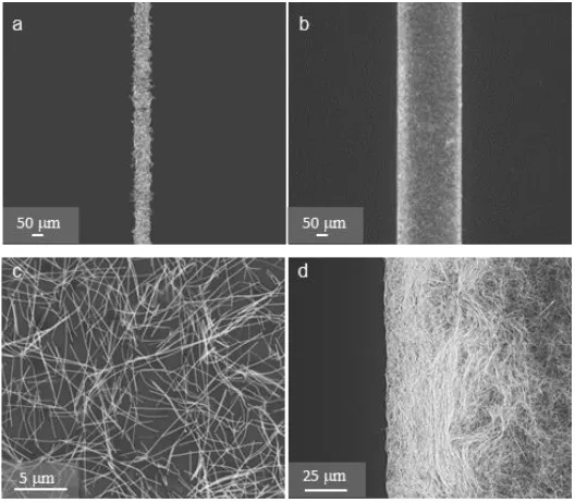
Figure S3.3. (a, b) Cross-sectional SEM images of a freeze-fractured AgNW/CF coating
(1 mg/mL) on a silicon wafer. The AgNW network resides at the surface of a ~30-
m-thick CF layer. ... 104
Figure S3.4. AFM height image (scale = 2 m, z-scale = 250 nm) with RRMS
measurements and corresponding profile measurement of AgNW network (2 mg/mL) on
silicon wafer without CF matrix. ... 105
Figure S3.5. Transmission spectrum of CF/PDMS composite. ... 106
Figure S3.6. Optical micrographs of the interface between CF and T-IIR substrate at (a)
0%, (b) 10%, and (c) 70% strain. Optical micrographs of the interface between CF and
PDMS substrate at (d) 0%, (e) 10%, and (f) 70% strain. The samples were stretched in
the horizontal direction. ... 106
Figure S3.7. Transmittance spectra of (a) T-IIR/[AgNW]1.0 and (b) PDMS/[AgNW]1.0
composites before (black lines) and after exposure to 45 °C/ 95% RH for 30 days (green
lines), immersed in water for 7 days (red lines), and exposure to nitric acid vapor for 24
hours (blue lines)... 107
Figure 4.1. AFM phase images of (a) RgP16, (b) RgP34, and (c) RgP69 films on
ITO/glass. AFM height images of (d) RgP16, (e) RgP34, and (f) RgP69 films on
ITO/glass. ... 116
Figure 4.2. (a) Optical micrograph, (b) AFM phase image, and (c) AFM height image of
PEO/LiCO3SO3/Ir films on ITO/glass. (d) Optical micrograph, (e) AFM phase image, and
xxviii
Figure 4.3. Optical micrographs of (a) RgP16/LiCF3SO3/Ir, (b) RgP34/LiCF3SO3/Ir, and
(c) RgP69/LiCF3SO3/Ir films on ITO/glass. AFM phase images of (d)
RgP16/LiCF3SO3/Ir, (e) RgP34/LiCF3SO3/Ir, and (f) RgP69/LiCF3SO3/Ir films on
ITO/glass. AFM height images of (g) RgP16/LiCF3SO3/Ir, (h) RgP34/LiCF3SO3/Ir, and
(i) RgP69/LiCF3SO3/Ir films on ITO/glass. ... 120
Figure 4.4. Temporal evolution of (a) radiance, (b) current, and (c) EQE of a typical rigid
LEEC fabricated from RgP16/LiCF3SO3/Ir (green), RgP34/LiCF3SO3/Ir (red), and
RgP69/LiCF3SO3/Ir (black) operated at 6 V DC in inert conditions. ... 123
Figure 4.5. Temporal evolution of radiance of (a) RgP34/LiCF3SO3/Ir LEECs and (b)
RgP69/LiCF3SO3/Ir LEECs after 0 cycle (black), 10 cycles (green), 30 cycles (red) and
50 cycles (blue) of 15% strain. ... 127
Figure S4.1. Diagram of the rigid LEEC test structure fabricated with an ITO-coated
glass anode, Ir based emissive material, and liquid EGaIn as the cathode. ... 133
Figure S4.2. Temporal evolution of radiance of a typical rigid LEEC fabricated from
pristine film of [Ir(ppy)2(dtb-bpy)]+[PF6-] operated at a 6 V DC in inert conditions. .... 133
Figure S4.3. Temporal evolution of radiance of a typical rigid LEEC fabricated from
film of PEO/LiCF3SO3/Ir composite operated at 6 V DC in inert conditions. ... 134
Figure S4.4. Optical micrographs of films of (a) PEO/LiCF3SO3/Ir composite, (b)
RgP16/LiCF3SO3/Ir composite, (c) RgP34/LiCF3SO3/Ir composite, and (d)
RgP69/LiCF3SO3/Ir composite on a PDMS substrate with stretching at 5 % strain. The
xxix
Figure S4.5. Temporal evolution of current of a typical rigid LEEC fabricated from film
of (a) RgP34/LiCF3SO3/Ir and (b) RgP69/LiCF3SO3/Ir composites operated at 6 V DC in
inert conditions. Temporal evolution of EQE of a typical rigid LEEC fabricated from film
of (c) RgP34/LiCF3SO3/Ir and (d) RgP69/LiCF3SO3/Ir composites operated at 6 V DC in
inert conditions... 135
Figure 5.1. (a) Optical and (b) SEM micrographs of patterned ENIG20 films on PDMS
substrate. (c) Optical and (d) SEM micrographs of an unpatterned ENIG20 film on PDMS
substrate. (e) Thickness as a function of IG time. (f) Rs as a function of IG time. ... 144
Figure 5.2. (a) Change in resistance of ENIG20 films as a function of tensile strain.
Optical micrographs of (b) ENIG20 film and (c) EBAu film on PDMS substrates at 10%
tensile strain. SEM micrographs of (d) ENIG20 films and (e) EBAu films on PDMS
substrates at 30% tensile strain. Higher magnification SEM micrographs of (f) ENIG20
film and (g) EBAu films on PDMS substrates at 30% elongation. Samples were stretched
in the horizontal direction. (h) XRD spectra of ENIG20 (black line) and EBAu films (red
line) on glass substrates. ... 149
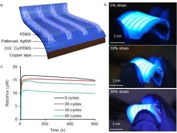
Figure 5.3. (a) Structure of ACEL device. Photographs of ACEL devices (3 cm x 3 cm)
bent to (b) 15% and (c) 40% strain. (d) Photographs of ACEL devices (1.5 cm x 3 cm)
stretched to 0%, 10%, 20%, 30% and 40% strain. (e) Change in emission radiance of the
ACEL devices under various stretching strains during three minutes of operation in
ambient conditions. ... 154
Figure S5.1. Optical micrographs of (a) 5 min, (b)10 min, (c)15 min, and (d) 20 min
xxx
Figure S5.2. Optical micrographs of (a) ENIG10 and (b) ENIG15 on PDMS substrate.
SEM micrographs of (c) ENIG10 and (d) ENIG15 on PDMS substrate... 163
Figure S5.3. Photographs of (a) ENIG10, (b) ENIG15, and (c) ENIG20 films before (left
column) and after (right column) tape test. ... 164
Figure S5.4. EDX of (a) ENIG10, (b) ENIG15, and (c) ENIG20 films on a silicon wafer.
... 165
Figure S5.5. SEM cross-sectional image of ENIG20 film on a silicon wafer. ... 166
Figure S5.6. (a) Optical and (b) SEM micrographs of EBAu films on PDMS. (c)
Photographs of EBAu film on PDMS substrate before (left) and after (right) tape test.
The marks on the gold film were left when it was taken off from the sample holder. ... 167
Figure S5.7. (a) AFM height image and (c) corresponding profile measurement of
ENIG20 film on a silicon wafer. (b) AFM height image and (d) corresponding profile
measurement of EBAu film on a silicon wafer. ... 168
Figure S5.8. Optical micrographs of (a) ENIG20 film and (b) EBAu film on PDMS
substrate at 80% tensile strain. ... 169
Figure S5.9. Patterned ENIG20 wires on PDMS substrate as stretchable interconnects for
LED circuits at (a) 0% and (b) 40% tensile strain. ... 169
Figure S5.10. (a) Change in maximum radiance of ACEL devices as a function of
repeated 40% strain cycles. (b) Resistance of PEDOT:PSS/Triton X-100 film on PDMS
xxxi
List of Abbreviations / Symbols
3D three-dimensional
%T percent transmittance
° degree
AC alternating current
ACEL alternating-current electroluminescence
AFM atomic force microscopy
AgNW silver nanowire
APTES 3- aminopropyltriehthoxysilane
bpy bipyridine
cc-mm/m2-day cubic centimeter-millimeter/meter squared-per-day
CNT carbon nanotube
DC direct current
dtb di-tert butyl
mechanical strain
ELD electroless deposition
e-beam electron beam
ECD electrochemical doping
ED electrodynamic
EDL electric double layer
EGaIn eutectic gallium-indium
EL electroluminescence
EQE external quantum efficiency
PF6 hexafluorophosphate
IIR isobutylene-co-isoprene rubber
xxxii
ITO indium tin oxide
Ir iridium
t1/2 lifetime of device
LEEC light-emitting electrochemical cell
MACP matrix-assisted catalytic printing
Rmax maximum radiance
CP micro contact printing
n-doped negatively doped
OLED organic light-emitting diode
p-doped positively doped
PDMS poly(dimethylsiloxane)
PEG poly(ethylene glycol)
PEO poly(ethylene oxide)
PET poly(ethylene terephthalate)
PI polyimide
PLEC polymer light-emitting electrochemical cell
PMMA poly(methyl methacrylate)
PMETAC poly[2-(methacryloyloxy)ethyl-trimethylammonium
chloride]
PEDOT:PSS
poly(3,4-polyethylenedioxythiophene)-poly(styrenesulfonate)
ppy phenylpyridine
MEH-PPV poly[5-(2’-ethylhexyloxy)-2-methoxy-1,4-phenylene
vinylene]
Psig pounds per square inch
PVD physical vapor deposition
R resistance
R/R0 change in resistance
xxxiii
RH relative humidity
RMS root-mean-squared
RRMS root-mean-square roughness
rpm rotations per minute
Rs sheet resistance
SAM self-assembled monolayer
SEM scanning electron microscopy
ton turn-on time
TCE transparent conductive electrode
T-IIR transparent poly(isobutylene-co-isoprene) rubber
UV ultraviolet
UV-Vis ultraviolet visible
XPS X-ray photoelectron spectroscopy
1
1. Chapter 1
2
1.1. Compliant Electronics
The global market for compliant electronics has had tremendous growth and is
expected to reach > $800 million USD dollars by 2023 from ~$28 million in 2017.1
Unlike traditional electronics that are made from rigid and bulky components, these
flexible and stretchable electronics are a new format of devices fabricated from materials
that retain their functionality even during mechanical deformation such as bending,
twisting, and stretching. These fully deformable devices open up new applications that
were previously impossible to achieve using conventional rigid materials such as
compliant energy harvesting systems,2 optoelectronics,3,4 sensors,5 actuators,6 artificial
skins,7 smart clothing,8 soft robots,9 and bioelectronics.10 This dissertation focuses on the
development of deformable, low-cost, electroluminescent (EL) devices.
1.2. EL Devices
Compliant lighting devices are expected to bring new possibilities that inspire
people’s imagination for a display-centric world in the future. With these technologies,
we could unfold and then hang a large-area screen on the wall to use, and then fold it into
our pockets when we are done. We could directly laminate light therapy devices made
completely from conformable materials to our human body and conduct the treatment
while we can still move freely. We could continuously monitor our health using a suite of
truly conformable health monitors distributed across the body without noticing their
existence. The advance of flexible and stretchable optoelectronics brings these types of
products closer to reality. One principle consideration for fabricating these compliant
3 layer in a multilayer stack such as the typical conventional organic light-emitting diodes
(OLEDs) consisting of eight individual layers responsible for charge injection, transport,
and emissive recombination (Figure 1.1a).11 Thus, new types of light-emitting devices
with a simple structure need to be designed.
Figure 1.1. (a) Structure of a typical OLED that contains eight layers of active materials. (b) Structure of a typical ACEL device and LEEC. Adapted with permission from reference 11.
Fortunately, researchers have developed two very promising light emitting
alternatives suitable for stretchability: Alternating-current electroluminescent (ACEL)
devices and light-emitting electrochemical cells (LEECs). These types of EL devices
sandwich a single layer of EL material that combines charge injection and transport
together between two electrodes (Figure 1.1b),12,13 and possess much simpler structures
compared to conventional OLEDs. Thus, it is easier to impart compliance into all three
layers and integrate these three components into one single stretchable EL device.
solution-4 processable, which lowers the fabrication cost. In the following sections, we will discuss
ACEL devices and LEECs in greater detail.
1.2.1.ACEL Devices
ACEL devices have been explored for display and lighting applications for almost
three decades.14 It sandwiches a layer of EL material between two electrodes, and is
driven by alternating voltage. The emissive material consists of two materials: an organic
or inorganic phosphor, the luminescent center that dominates the optoelectronic
properties of the emissive material, and an insulator, the host material that dominates the
electrical properties of the emissive material.15 The commonly used phosphor is
inorganic ZnS doped with different impurities such as Cu, Mn, and Al to achieve various
emission colors including red, blue, green, and white.16
In these devices, the light originates from field-induced luminescence in the
following sequence: charge injection into the phosphor layer upon the application of AC
voltage beyond threshold, typically from 150 V to 250 V,14 acceleration of the electrons
to high energies under high electrical field and then excite luminescent centers to form
excitons, and radiative relaxation of the luminescent center.17 The high operating voltage,
however, likely stunts their applications in portable and wearable electronics.
1.2.2.Light Emitting Electrochemical Cells (LEECs)
The concept of the LEEC was first introduced by Pei and coworkers in 1995.18
LEECs possess a similar device structure to ACEL devices with an emissive layer
sandwiched between two electrodes. The emissive material consists of an ionic EL
5
1.2.2.1.Working Mechanism of LEECs under DC Voltage
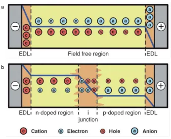
Studies have revealed two working mechanisms for LEECs: electrodynamic (ED)
model20-23 (Figure 1.2a) and electrochemical doping (ECD) model (Figure 1.2b).18,24-27
Both models agree that separating the cations and anions in the EL layer upon application
of a voltage reduces the electron and hole injection barrier.
The ED model assumes that upon the application of a voltage above the threshold,
charged ions begin to migrate and are redistributed at the respective electrode interfaces
to form electric double layers (EDLs). The EDLs induce a sharp drop of the electric
potential near the electrode interfaces and lower the charge injections barrier. Once the
injection barrier is reduced, significant numbers of electrons and holes are injected into
the emissive material leading to the oxidation and reduction of the emissive material in
the bulk of the material. The oxidized and reduced species are then recombined together,
emitting light in a field-free region.
The ECD model also assumes that the accumulation of ions at anodes and
cathodes leads to the formation of EDLs at the electrodes. The injection of electrons and
holes at the cathode and anode respectively also causes the development of positively
doped (p-doped) and negatively doped (n-doped) regions in the bulk. The counter ions
migrate to neutralize the charge. The doped regions expand over time until a negative
doped-intrinsic undoped-positive doped junction between them forms. Across the
intrinsically undoped region, the applied potential drops substantially and charges
recombine and emit light.
A recent study, however, shows that both the ECD and the ED model are valid
6 limited electrons inject into the EL material, and then the ECD model prevails when
substantial electron injection occurs.28 The doped region continuously grows toward
each other at the expense of the undoped area, which causes the quenching of excitons
and leads to a decline in EL intensity and efficiency.29 The speed of forming the EDL
determines the turn-on time of LEECs, and the growing rate of the doped zone is directly
related to the lifetime of LEECs. Both speeds are determined by the electronic and ionic
mobility, the applied voltage and the thickness of the emissive layer.30
Figure 1.2. Illustration of potential profile and electronic along with ionic charge distribution in a LEEC during steady-state operation for the (a) ED model and (b) ECD model.
7
1.2.2.2.Figures of Merit
A set of figures of merit are used in order to quantify the performance of LEECs
with different EL materials. The commonly used figures of merit include:
1. Maximum radiance (Rmax): Maximum flux of light emitted by LEECs,
measured in Watts.
2. Turn-on time (ton): Time it takes for the device to emit light above a particular
threshold. While some researchers define this as the time for the onset of light emission31
or the time it takes to reach the Rmax,12 we define this as the time it takes for the device to
reach ~10 nW radiance.
3. tmax: Time it takes for the device to reach the Rmax.
3. External quantum efficiency (EQE): The ratio of emitted photons to the total
amount of injected electrons.
4. Lifetime (t1/2): The time it takes for the device radiance to decay to one half of
its maximum value.
1.2.2.3.Classification of LEECs
LEECs are classified into two categories according to the difference in the
composition of light-emitting material: polymer LEECs (PLECs) and ionic transition
metal complex LEECs (iTMC-LEECs).12,19
The active layer of a PLEC is a mixture of electronic and ionic conductors. The
conjugated polymer, such as poly[5-(2’-ethylhexyloxy)-2-methoxy-1, 4-phenylene
8 and the solid-state electrolyte, typically consisting of an ion-solvating polymer such as
poly(ethylene oxide) (PEO) and a lithium salt, acts as the ionic conductor to provide
mobile ions (Figure 1.3a).33 By changing the active conjugated polymer, PLECs emitting
red, blue, green, yellow, and even white light have been reported.18,34-36
Figure 1.3. (a) Materials used in the first PLEC: conjugated polymer of MEH-PPV, ionic conductors of PEO and lithium trifluoromethanesulfonate salt. (b) The first [Ru(vbpy)3](PF6)2 RuII-iTMC
used for LEECs. (c) Structure of [Ir(bpy)3]+ (bpy = bipyridine), a sample of the largest class of IrIII-iTMCs
used in LEECs. Adapted with permission from reference 11.
iTMC-LEECs require a single iTMC as the emissive material since the ionic
nature of iTMC allows it to act as both ionic and electronic conductors. The light
emission occurs by phosphorescence, originating from long live-triplet excitons, and can
be quenched by electrochemical doping. In 1996, Maness et al.37 and Lee et al.38 report
the first iTMC-LEECs made from [Ru(vbpy)3](PF6)2 (vbpy =
4-vinyl-4'-methyl-2,2'-bipyridine) that emitted orange light (Figure 1.3b). Nowadays, research on iTMC-LEECs
is mostly based on luminescent ionic biscyclometalated IrIII complexes39 since they can
emit various colors due to the easily tunable band gap of these molecules.40 Figure 1.3c
9
1.2.2.4.Challenge of LEECs
As discussed in Section 1.2.2.1, the ion conductivity in the emissive material
strongly influences the optoelectrical performance of LEECs. Mobile ion is essential for
the redistribution of ions to form EDLs to promote the electron injection. The turn-on
time of LEECs is directly determined by the speed of the formation of EDLs; the lifetime
of LEECs is dominated by the growing speed of the doped regions, both of which are
influenced by the ion conductivity. However, the low ion conductivity in the solid state
compared to that in the liquid state results in a delay period (few seconds to several
hours) for LEECs to become operative, which is an obstacle for most practical
applications that require instant response. Several strategies have been reported to
overcome this drawback. The first approach directly adds ionic conductors to the
light-emitting material to increase the ion conductivity. Costa et al. and Parker et al. mixed
iridium iTMCs with an ionic liquid and demonstrated that the tmax or ton of LEECs
fabricated from these iTMCs/ionic liquid composites were decreased by one order of
magnitude.31,41 Lyons et al. and Pei et al. blended poly(ethylene oxide)/lithium
trifluoromethanesulfonate (PEO/LiCF3SO3), a known solid electrolyte, into either
ruthenium iTMC or conjugated polymer to enhance the ion conductivity. The ton was
within a few seconds after incorporating the solid electrolyte into the emissive
material.18,40 The second strategy is to increase the device driving voltage.37,42,43 The high
driving voltage reduces the charge injection barriers as well as increases the ion
movement speed, resulting in a faster build-up of the EDLs and thus lowering the ton.
Although increasing ion conductivity can reduce the ton, it also reduces the device
10 causes a quicker exciton quenching and a faster degradation of the emissive materials.
Thus, there is a trade-off between the turn-on time and the lifetime. It is crucial to adjust
the ion conductivity of the light-emitting materials in order to balance the trade-off effect.
To prepare compliant EL devices, each layer in the device needs to remain soft
and functional with deformation. In the following sections, we will explore methods to
incorporate compliance into each layer of ACEL devices and LEECs.
1.3. Strategies to Incorporate Compliance in Transparent
Conductive Electrode (TCE)
The transparent conductive electrode (TCE) is a crucial component of compliant
optoelectronics and largely dictates their mechanical deformability and electrical
performance. It not only acts as a window for light to enter or leave in devices but also
remains conductive under mechanical stress. Several figures of merit are employed to
judge the performance of TCEs made from different materials, which include:
1. Transmittance (T%): Transparency of the material over the visible
wavelengths. It is used to characterize the optical property of the TCE. In general, high
T% is desired for TCE applications. Typically, researchers report the transmittance at a
wavelength of 550 nm since it is in the middle of the visible-light wavelength.
2. Sheet resistance (Rs): A measurement of the resistance of a thin uniform sheet,
analogous to density, that is invariable under scaling of the sheet size, and is used to
compare how conductive a material is regardless of size. Material with a lower Rs value
11
3. Surface roughness: A measurement that quantifies the deviations in the surface
smoothness of a film and is often expressed as root-mean-square roughness (RRMS) which
is an averaging method. RRMS plays an important role in thin-film devices by affecting
both the film quality and the device performance. In TCEs, specifically, RRMS can
influence the optical and electrical properties: Rougher surface results in more light
scattering and thus lower the transparency of TCE; it also leads to potential electrical
shorts if the protruding part of the electrode penetrates through the functional layer and
makes contact with the other electrode. Thus, a low RRMS is preferred in thin TCEs.
Other features that are important for the development of compliant TCEs include
good conductivity at high bending and stretching strains; durability to repetitive strains;
high throughput patterning methods; and inexpensive fabrication.
Indium tin oxide (ITO) is universally employed in rigid optoelectronic devices
due to its excellent transparency (≥ 80%), low Rs (10 ~40 /sq), and low surface
roughness (< 10 nm).44-47 However, its brittle nature limits its application as a TCE in
flexible or stretchable electronics.48 Although depositing ITO on a flexible substrate such
as polyethylene terephthalate (PET) slightly increases its flexibility from < 1% to < 5%
before electrical failure, the low processing temperature of PET substrate results in
insufficient conductivity of the resulting ITO film.49 In addition, the slow sputtering
process (linear coating rate of ~0.01 m/s) decreases the throughput rate and thus, raising
the fabrication cost.50
Extensive research has been devoted to replacing the ITO based TCE with one
that can deliver the same high conductivity and transparency, combined with the ability
12 substitution include carbon nanotubes,51,52 graphene,53 conductive polymers,54 metal
grids,55 and random meshes of nanowires.56,57 Silver nanowires (AgNWs) are considered
to be a very promising replacement for ITO due to intrinsically low Rs (as low as <1
/sq) and high transparency (as high as > 90%).58 Randomly arranged AgNWs form an
interconnected percolation network, creating pathways for electrons to migrate and thus
result in a conductive network (Figure 1.4a). The gaps among AgNWs allow light to pass
through and thus make the network transparent. We can easily alter the transparency and
conductivity of AgNWs with a certain diameter and length by controlling the density of
AgNWs deposited on the substrate.58 Additionally, the AgNWs dispersed in a solvent
such as water and ethanol can be used as an ink for low-cost and high throughput
processing such as roll-to-roll (R2R) techniques,59,60 making it a practical printable
conductor. The contact resistance between individual AgNWs increases the overall Rs of
the AgNW network and is undesirable for TCEs.61 To lower the contact resistance
between AgNWs, annealing is used to fuse the AgNW-AgNW junctions.57,62,63 Thermal
annealing of AgNW networks at a temperature of 200 ºC results in the reduction of Rs by
several orders of magnitude (Figure 1.4b).62,63 Moreover, this annealing temperature is
compatible with both plastic substrates, such as PET, polyimide, and poly(ethylene
naphthalate) (PEN), and elastic substrates such as poly(dimethylsiloxane) (PDMS),
making AgNWs suitable for the fabrication of flexible and stretchable TCEs.
13
Figure 1.4. (a) SEM image of AgNW network. Scale bar = 1 m (b) Change in resistance as a function of thermal annealing temperature. The concentration of AgNW dispersion is 0.75 mg/mL and the
deposited density is 105 mg/m2. Adapted with permission from reference 62.
1.3.1.Strategies to Prepare Flexible AgNW-TCEs
The inherently high aspect ratio of AgNWs makes them intrinsically flexible and
enables the feasible fabrication of flexible TCEs by depositing AgNW dispersion on a
flexible substrate such as PET64-67 or PEN.68 The good dispersity of AgNWs in solvents
such as water and ethanol allows the fabrication of AgNW films using various
solution-based deposition methods including drop casting,57,69 spin coating,70,71 spray coating,72,73
vacuum filtration,74 and Meyer-rod coating.75 As the demand for low-cost fabrication
methods keeps increasing, the R2R process attracts researchers’ attention. The production
cost can be reduced to a fraction of the cost of traditional semiconductor manufacturing
methods due to its high throughput.59,60,76
Unfortunately, AgNW films produced by many of these techniques have two
main issues: poor adhesion to the underlying substrate77 and high surface roughness due
to irregular piles of AgNWs with individual AgNWs protruding > 100 nm from the
14 from the surface by touching or scratching. The high surface roughness not only lowers
the efficiency of optoelectronics but also increases the risk of potential short circuits by
causing contacts between two electrodes, or damaging layers with localized high electric
fields.
Figure 1.5. (a) Cross-sectional SEM image of AgNWs protrusion from the surface of a substrate. (b) AFM profile measurement of a AgNW film on a silicon wafer. (c) Cross-sectional SEM image of
AgNW-OA coating on a glass substrate. (d) Top view SEM image of a AgNW-AgNW-OA coating surface. Adapted with
permission from reference 78 (a) and 74 (b-d).
One widely used solution to decrease the surface roughness is to embed AgNWs
15 followed by transfer of the AgNW/polymer composite to the target substrate. The
polymer fills in the voids among AgNWs and results in a smooth surface. Additionally,
the polymer adheres to the AgNW network, enhancing the mechanical flexibility. For
example, Miller et al. produced a uniform AgNW network by vacuum filtering and
embedded it in a transparent polyurethane optical adhesive (OA).74 The AgNW
composite adheres strongly to the underlying substrate and is durable, resisting marring,
scratching and solvent exposure. Similarly, Liang et al. used Meyer rod or airbrush to
produce AgNW network on a glass substrate followed by transferring it into a
polyurethane acrylate matrix.80 Kim et al. embedded AgNW network in the polyurethane
urea matrix to decrease the surface roughness of the AgNW composite.81 The resulting
AgNW composites with uniform and smooth surfaces were embedded in, and not
protruding from the surface of polymer matrix (Figure 1.5c, d).
1.3.2.Strategies to Prepare Stretchable AgNW-TCEs
One major strategy to improve the stretchability of AgNWs based TCEs is to
embed AgNWs into a stretchable polymer matrix such as polyacrylate,82 polyurethane,83
and poly(urethane acrylate).80 This polymer matrix functions the same as the polymer
matrix in the flexible AgNW-TCEs while significantly increasing the stretchability of the
resulting AgNW-polymer network. Yu et al. embedded AgNWs in a polyacrylate matrix
to prepare an elastic TCE with a transmission of 45% at 550 nm and a stretchability of
16% strain at room temperature.84 Hu et al. further improved the optical, electrical and
mechanical properties of the AgNW/polyacrylate composite by incorporating an aromatic
16
resulting composite showed a transmission of 79.6% with a Rs of 7.5 /sq and remained
conductive up to 80% elongations.
1.3.3.Strategies to Prepare Patterned AgNW-TCEs
Applications such as displays and touch screens require patterned electrodes.
Thus, to realize the practical use of AgNW-TCEs in a compliant display, we need to
develop patterned and soft AgNW films with various feature sizes.
Various patterning techniques have been demonstrated to produce patterned
AgNW films. Madaria et al. used a dry transfer technique to produce patterned
AgNW-TCE. They first fabricated a PDMS stamp with repeating 1-mm-length square patterns,
and then used this stamp to selectively pick up AgNWs on an aluminum oxide membrane
and pressing them to the target PET or glass substrate.85 The patterned AgNWs exhibited
the same features as the PDMS stamp, and the minimum dimension was defined by the
dimension of the PDMS stamp. Ko et al. employed a photolithographic method to
produce AgNWs with circle and line patterns on a glass substrate.86 Drop casting a
poly(ethylene glycol) (PEG) precursor on top of a deposited AgNW network and then
selectively gelating the PEG through a photomask under UV light enables the transfer of
the cured PEG gel along with the underlying AgNWs to a target substrate, leaving the
uncured PEG on the carrier substrate. The generated patterns had a minimum dimension
of 200 m. Liang et al. screen printed a layer of AgNWs from a dispersion in methanol
through a shadow mask on a glass substrate to obtain patterned AgNW lines with a
dimension of 100 m x 5000 m.87 Tybrandt et al. filtered an AgNW dispersion through
17
photoresist, patterned AgNWs with dimension as small as 10 m were left on the PVDF
membrane, which was then transferred to a PDMS substrate. Song et al. produced
patterned AgNW grids on plastic substrate such as PET, PEN, and colorless-polyimide
(cPI) utilizing a two-step intense-pulsed-light (IPL) irradiation: first, irradiation of the
AgNW network with IPL through a photomask using a high voltage (2.5 kV for PET and
PEN, 3.0 kV for cPI); and second, removal of the nonradiated AgNWs using either
ultrasonication or a commercial tape.89 The appropriate IPL irradiation time caused the
welding of AgNWs while too long IPL irradiation time damaged the AgNW network.
1.3.4.Challenge of AgNW-TCEs: Degradation of AgNWs
When the scale reduces to the nanometer, the high aspect ratio of AgNWs
provides a significantly large surface area to react with oxygen and sulfur, thus
accelerating the silver corrosion process.90,91 Previous studies have shown that AgNWs
break into small rods or particles after reacting with oxygen and sulfur-containing gases
(Figure 1.6a, b) and undergo electrical failure in only a month when storing in
atmosphere and even shorter lifetime when exposed to harsh environments.90,92-94 This
poor stability makes it challenging to employ bare AgNWs for any realistic applications.
A barrier layer has been employed to coat individual AgNW or fully overcoat the
entire AgNW network to delay the degradation process of AgNWs. Coating the surface
of each individual AgNW with a protective material such as metal,95,96 metal oxide,97 and
photoresist98 forms a core-shell structure (Figure 1.6c). The outer shell shields the inner
AgNW core from interacting with the destructive environment and therefore protects it
from corrosion. Eom et al. electrodeposited a nickel shell on the exposed surface of


![Figure 3.1. Top view SEM images (scale = 5 T-IIR/[AgNW]nm) with RIIR/[AgNW]m) of (a) T-IIR/[AgNW]0.5, (b) T-IIR/[AgNW]0.7, (c) 1.0, and (d) T-IIR/[AgNW]2.0 composites](https://thumb-us.123doks.com/thumbv2/123dok_us/1350882.1167961/116.612.144.507.322.578/figure-images-scale-agnw-riir-agnw-agnw-composites.webp)
![Figure 3.2. Transmittance spectra of (a) T-IIR/[AgNW]n and (b) PDMS/[AgNW]n composites](https://thumb-us.123doks.com/thumbv2/123dok_us/1350882.1167961/119.612.199.449.73.384/figure-transmittance-spectra-iir-agnw-pdms-agnw-composites.webp)
![Figure 3.3. Resistance as a function of tensile strain of (a) T-IIR/[AgNW]PDMS/[AgNW]n and (b) n composites, where n = 0.5 mg/mL (black lines), 0.7 mg/mL (blue lines), 1.0 mg/mL (red](https://thumb-us.123doks.com/thumbv2/123dok_us/1350882.1167961/121.612.207.446.75.376/figure-resistance-function-tensile-strain-agnw-composites-lines.webp)

