Available online:
https://edupediapublications.org/journals/index.php/IJR/
P a g e | 1191
Simulation of Single Phase Seven Level Cascade
H-Bridge Multilevel Inverter & Modeling of
Switching and Conduction Losses
KODURU KUMAR M-tech Student Scholar [email protected]
QIS COLLEGE OF ENGINEERING & TECHNOLOGY DEPARTMENT OF ELECTRICAL & ELECTRONICS
ENGINEERING Ongle, prakasam ap A.P, India.
.
J.KRISHNA KISHORE Assistant Professor [email protected]
QIS COLLEGE OF ENGINEERING & TECHNOLOGY DEPARTMENT OF ELECTRICAL & ELECTRONICS
ENGINEERING Ongle, prakasam ap A.P, India.
Abstract— Multilevel power electronic converter has wide range of applications. In multilevel power electronic converters the output can be synthesized by combining several DC voltage sources. Cascade H-Bridge multilevel inverter generally requires more number of DC sources. An alternative option is to replace all the DC sources feeding H-Bridge cells with capacitors, leaving only one H-H-Bridge cell with a real DC sources. This paper presents a multilevel inverter model working in H-bridge topology. The multilevel model comprises of several H-bridge models consisting of MOSFET/IGBT that are cascaded to get desired number of levels. The inverter is fed from existing AC supply which is rectified and fed to inverter.The inverter has been controlled using selective harmonic elimination in which the switching angles were determined using the particle swarm optimization Algorithm (PSO). The PSO is a relatively new and powerful intelligent evolution algorithm for solving optimization problems. It is a population-based approach.Simulation studies are carried out in MATLAB/SIMULINK and the performance parameters of the proposed inverter are computed.
Index Terms—Cascaded H-Bridge Multilevel Inverter
(CHBMLI), Conduction Losses, Switching Losses, Selective Harmonic Elimination (SHE).
I. INTRODUCTION
Neutral point clamped topology was the first multilevel inverter (MLI), proposed by Nabae et al. [1]. The MLI topologies can be categorized in three basic groups: the neutral point clamped (NPC) MLI, flying capacitor (FC) MLI, and cascaded H-bridge (CHB) MLI [2]. The CHB MLI consists of a number of H-bridge units. The final output voltage is synthesized by the combination of the input dc voltages of all series connected units. H-bridge units may have low voltage components. This topology has a modular characteristic, since all the units are similar and the control strategy is the same for all the units. Therefore, it is very easy to replace if any unit becomes faulty. Even without discontinuing the load, it is possible
to bypass the faulty module by applying an efficient control technique. The CHB topology can be divided into two groups: symmetric structure and asymmetric structure. In the case of the symmetric structure, there are equal dc sources and N-numbers of H-bridge cells per phase arm. The number of levels in the output voltage should be 2N+1. All the units are similar. Each unit consist of four switches and one isolated input dc source, which can be obtained by single-phase or three-phase diode based rectifier arrangement [3]. Transformers are used to ensure proper electrical isolation. Nowadays, high frequency link transformer (HFL) based modules have been used for efficient design. During high power applications the conventional diode rectifier based dc–dc converters become bulky, but a high frequency link dc–dc converter reduces the size of the transformer. These HFLs are also well suited for regenerative applications.
The diode-clamped inverter uses a single dc bus that is subdivided into a number of voltage levels by a series string of Capacitors. A matrix of semiconductor switches and diodes allows each phase-leg output to be switched to any of these voltage levels. Pulse width-modulation (PWM) principles for this topology are fairly well established, but some modification of the basic modulation process is generally required to maintain balanced dc voltages across the series Capacitors using redundant switching states. The third important multilevel topology is the cascade H-bridgeinverter.
Available online:
https://edupediapublications.org/journals/index.php/IJR/
P a g e | 1192 and protection requirements of each bridge are modular.
However, each single-phase inverter requires its own isolated dc supply, typically derived from a multi-winding low-frequency transformer or high-frequency dc-to-dc converters. This complexity has generally restricted cascaded Inverters to the higher power range where several switched output voltage levels are needed and a diode-clamped structure is unsuitable because of the difficulty of balancing the series dc capacitor voltages. [4] The application of this tool in power systems is wide ranging. For example, [5] focuseson the problems of fuel cost minimization, voltage profile improvement and voltage stability enhancement. In [6], the hybrid model was employed for loss power minimization. The PSO is a relatively new and powerful intelligence evolution algorithm for solving optimization problems. It is a population-based approach [7-8]. The PSO was originally inspired by the social behavior of bird flocks and fish schools. It was observed that they take into consideration the global level of information to determine their direction. Hence, the global and the local best positions are computed at each instant of time (iteration), and the output is the new direction of search. Once this direction is detected, it is followed by the cluster of birds.
II. CASCADED H-BRIDGE MULTILEVEL INVERTER
While Diode-Clamped (DC-MLI) and Flying Capacitor (FC-MLI) are widely used for industrial medium voltage high power applications when just low number of levels (typically three) is required, Cascaded H-Bridge inverters (CHB-MLI) are most suitable for high voltage-high power, HVDC utility applications. Mainly due its modular structure which can be extended for high number of levels with no much complexity. Furthermore, with CHB-MLI, higher power and voltage capability can be achieved at lowest number of required devices compared to DC-MLI and FCMLI. The CHB-MLI uses series connection of single phase h-bridge inverters with separate dc sources. The main idea is that each bridge cell will generate three different voltages and the output waveform can be synthesized by the sum of the voltages generated by each cell. The separate dc sources might be solar panel PV cells or fuel cells.[1]
In this paper, a 7 Level CHB-MLI has been chosen to be investigated. The circuit layout for single phase 7-Level CHB-MLI is shown in Figure (2). The switching devices have been selected to be of IGBT type FZ1500R33HL3, which has a blocking voltage capability of 3.3 kV, and a maximum forward current of 1500 A and its shown in Figure(2). Datasheet for this type IGBT is
given in [9]. Typical applications of this IGBT are: Chopper Applications, Medium Voltage Converters, Motor Drives, Traction Drives, UPS Systems and Wind Turbines [9]. Each cell is connected to a dc link supply of 100 V. Modulation index of (0.8) was used throughout the analysis. The inverter has been modelled in MATLAB-SIMULINK with main objective of precisely calculating the conduction and switching losses of the inverter.
Fig.2. Single-phase 7-level cascaded h-bridge inverter circuit layout.
III. SELECTIVE HARMONIC ELIMINATION
Available online:
https://edupediapublications.org/journals/index.php/IJR/
P a g e | 1193 switching [4]. In addition, it can eliminate the dominant
low order harmonic and hence minimize the size of the required filter at the inverter output.
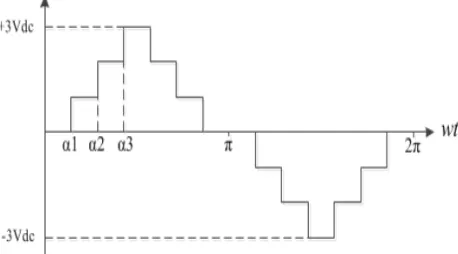
SHE uses pre-defined switching angles to form the desired multilevel fundamental voltage and eliminate the predominant low order harmonics which results in minimizing the total harmonic distortion (THD). The switching angles are precalculated off-line and hence this is considered open loop control technique. Figure (3) shows the stepped-voltage waveform for 7-level CHB-MLI. It is clear that, there are 3 switching angles which can be pre-calculated in this case.
Fig. 3. Stepped-voltage waveform for 7-level inverter.
Applying Fourier’s expansion, the stepped voltage wave form can be expressed in sum of sine and cosine periodic signals and a constant. The signal consists of odd and even harmonics. Due to the quarter symmetry of the waveform, the even harmonics and the dc constant are cancelled. Hence, only odd harmonics are considered. For balanced three phase systems all triplen harmonics are zero. Generally, the output voltage waveform can be written as:
(1) Where (S) is the number of H-bride cells of the inverter. It is clear from Figure (3) that all switching angles are less than 90°, and are all in ascending order. In 7-level CHB-MLI case,
(2) And it is possible to eliminate the 5th and 7th harmonic by solving the following system of non-linear equations where (mi) is the modulation index.
(3)
(4)
(5) Newton-Raphson iterative method has been applied to solve such system in practice. Key issue is that when the inverter level gets higher, it becomes more difficult to get to the solution. In addition, it requires good initial guessed values of the switching angles. In this paper, particle swarm optimization algorithm(PSO) has been applied to solve the system of transcendental equations [8]. The objective function is to minimize the total harmonic distortion (THD) with the transcendental equations (3-5) are set to be minimization constraints. This should result eliminating the 5th and 7th harmonics. The optimum switching angles of the 7-level CHB-MLI under investigation at 1.0 modulation index are found to be 11.5° , 28.7° and 57.2° respectively using PSO in Matlab.
IV. PARTICLE SWARM OPTIMIZATION ALGORITHM
In the basic particle swarm optimization algorithm, particle swarm consists of “n” particles, and the position of each particle stands for the potential solution in dimensional space. The particles change its condition according to the following three principles:
(1) to keep its inertia
(2) to change the condition according to its most optimist position
(3) to change the condition according to the swarm’s most optimist position.
The position of each particle in the swarm is affected both by the most optimist position during its movement (individual experience) and the position of the most optimist particle in its surrounding (near experience). When the whole particle swarm is surrounding the particle, the most optimist position of the surrounding is equal to the one of the whole most optimist particle; this algorithm is called the whole PSO. If the narrow surrounding is used in the algorithm, this algorithm is called the partial PSO.
Each particle can be shown by its current speed and position, the most optimist position of each individual and the most optimist position of the surrounding.
Available online:
https://edupediapublications.org/journals/index.php/IJR/
P a g e | 1194 V. POWER LOSS MODELLING
When operating power electronics devices that involve switching of semiconductor devices, there are mainly four types of power losses occur during this operation. These types are: 1) Conduction losses, 2) Switching losses, 3) OFF-state losses, and 4) Gate losses. The Off-state and Gate losses are very small and normally neglected. Hence, in this paper, only conduction and switching losses have been considered for the analysis.
Compared to two level inverters, the estimation of inverter losses is a complicated task for multilevel inverters. The usual conventional methods used to calculate the losses in two level inverters, are not suitable to be applied in the case of multilevel inverters. Main reason for this is that in multilevel inverters, each semiconductor devise has different current compared to other devices which implies different losses behavior for each one. This results from having different on-state ratio for each device for one leg during one period of output phase voltage. Furthermore, at higher number of levels, the switching frequency of each device is not the same which add more complexity to the estimation method.
In this paper, a simplified model is proposed for calculating the losses of CHB-MLI precisely. The proposed model uses the method applied in [3] with little modifications. The operating temperature is assumed to be maximum at 150ஈ. The model is based on on-line calculation in which MATLAB-SIMULINK software has been used for the modelling. Mixed load of R=60 ȍ and L=20 mH , has been considered for the analysis. The result compared to the case where the load is changing from purely resistive load gradually to purely inductive load. The purpose is to provide a comprehensive study of the inverter losses behavior at different load conditions.
A. Conduction Losses
For a semiconductor device, the losses which occur while the power device is on the on-state and conducting current, is defined to be the device conduction losses. In CHB-MLI, the conduction loss increases proportionally with the number of cascaded cells. At conduction, the power dissipation can be computed by multiplying the on-state saturation voltage by on-state current.
(6) The absolute value is taken as the conducting current is always positive for the device. Most of the literatures usually are modelling the on-state voltage by inserting a voltage Vo, representing the voltage drop of the device called threshold voltage, and a resistor ron representing
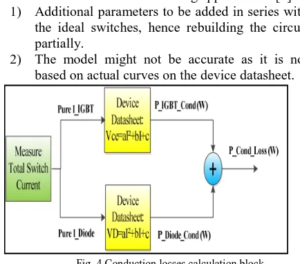
the current dependency in series with the ideal device. The main drawbacks of this modelling approach are [3]:
1) Additional parameters to be added in series with the ideal switches, hence rebuilding the circuit partially.
2) The model might not be accurate as it is not based on actual curves on the device datasheet.
Fig. 4.Conduction losses calculation block. In the proposed model, the conducting losses are computed in much easier and more efficient way. The on-state voltage is represented by a quadratic equation in terms of the on-state current. The quadratic equation is obtained using curve fitting tool based on the actual curves in the device datasheet. For each power device, there will be two quadratic equations, one for the switch and one for the diode. Hence, in the MATLABSIMULINK model, the pure switch current and pure diode current need to be obtained separately. By plotting the onstate device current, the positive portion is representing the pure switch current and the negative portion is representing the pure diode current. Having these currents separated, the conducting losses for the IGBT switch and the diode can be obtained simply by applying the following blocks.
B. Switching Losses
The switching loss can be defined as the power dissipated during the turn-on and the turn-off switching of the power semiconductor device. It occurs on both the switch and the antiparallel diode. The switching loss is highly proportional to the switching frequency, and hence it contributes substantially to the inverter total loss especially for inverters using SPWM. For the power switch, there are the turn-on loss (Eon) and the turn-off loss (Eoff). On the other hand, for the antiparallel diode, only the off (Erec) loss is considered while the turn-on loss is normally neglected due to fast cturn-onducting of the diode when it get forward biased. The turn-on loss is less than 1% compared to the turn-off loss in modern diodes.
Available online:
https://edupediapublications.org/journals/index.php/IJR/
P a g e | 1195 resistor and wiring stray inductance [3]. The switching
loss is considered a major drawback in multilevel inverters causing high increase in cost and reducing efficiency in HVDC applications.
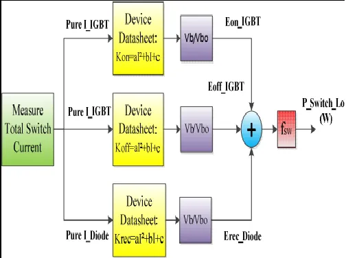
This paper proposes an online estimation of switching losses based on the switching energy curves given in the device datasheet. Energy factor curve (K) is obtained by dividing the energy by switching current. Then Curve fitting tool is used to approximate the energy factor curves by second order polynomials. Multiplying the energy factor curve equation by the switching current should give the energy loss which further multiplied by the switching frequency to get the power loss. In case, the blocking voltage is different, a normalization factor is used to adjust that in the loss calculation. Figure 5 shows the block implemented for the switching loss calculation. The complete block for the proposed modelling of losses calculation in CHB-MLI is presented in Figure .6.
Fig.5. Switching losses calculation block.
Fig.6. Basic flow Model of Proposed Methodology for Losses Calculation in CHB-MLI.
V.MATLAB/SIMULATION RESULTS
Fig.7.Matlab/Simulink Model of Seven Level Inverter.
Available online:
https://edupediapublications.org/journals/index.php/IJR/
P a g e | 1196 Fig. 7.2 Conduction and switching losses of cell
Fig 7.3 Conduction loss calculation
Fig 7.4 Switching loss calculation
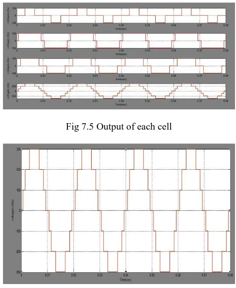
Fig 7.5 Output of each cell
Fig 7.6 Single phase 7level output
VI.CONCLUSION
The multilevel inverter advantages have been achieved after applying in industrial and utility applications. CHB-MLI is widely applied compared to other topologies. It is critically important to evaluate the losses in multilevel inverters as accurate as possible. Among the many types of losses in multilevel inverters, conduction and switching losses are the most dominant. In this paper, a simple, efficient and easy to implement on-line method for conduction and switching losses calculation in CHB-MLI, has been presented. The model evaluates the losses by calculating the conduction and switching losses in each device separately. Then, adding the losses together.
REFERENCES
[1] N. Mittal, B. Singh, S.P. Singh, R. Dixit and D. Komar, “Multi-Level Inverter: a Literature Survey on Topologies and Control Strategies”, ICPCES, 2nd International Conference on Power, Control and Embedded Systems, 2012.
Available online:
https://edupediapublications.org/journals/index.php/IJR/
P a g e | 1197 [3] Uwe Drofenik, Johann W.Kolar. “ A general Scheme for Calculating
Switching- and Conduction Losses of Power Semiconductors in Numerical Circuit Simulations of Power Electronic System”, Proc. Of the 5th Int. Power Electron. Conference, Niigata, Japan (2005-4). [4] M.G.H. Aghdam, S.S. Fathi and A. Ghasemi, “The Analysis of Conduction and Switching Losses in Three-Phase OHSW Multilevel Inverter Using Switching Functions”, IEE PEDS 2005, Vol. 1, pp. 209-218, 2005.
[5] J. Ramu, S. Parkash, K. Srinivasu, R. Ram, M. Prasad and Md. Hussain, “Comparison between Symmetrical and Asymmetrical Single Phase Seven Level Cascaded H-Bridge Multilevel Inverter with PWM Topology”, IJMSE, Vol.3, No.4, pp.16-20 April 2012.
[6] Farzaneh, A.; Nazarzadeh, J. , "Precise Loss Calculation in Cascaded Multilevel Inverters," Computer and Electrical Engineering, 2009. ICCEE '09. Second International Conference on , vol.2 , pp.563-568, 28-30 Dec. 2009
[7] C. Govindaraju1 and K. Baskaran, “Performance Improvement of Multiphase Multilevel Inverter Using Hybrid Carrier Based Space Vector Modulation”, International Journal on Electrical Engineering and Informatics - Volume 2, Number 2, 2010,pp 137-149.
[8] D. Kumar, S. Pattnaik and V. Singh “Genetic Algorithm Based Approach for Optimization of Conducting Angles in Cascaded Multilevel Inverters”, IJERA, Vol. 2, Issue 3, May-Jun 2012, pp.2389- 2395.
[9] Infineon: Datasheet of IGBT module “FZ1500R33HL3 “published at:http://www.infineon.com/cms/en/product/power/igbt/igbtmodule/igbt module3300v/FZ1500R33HL3/productType.html?pro uct Type=db3a3 04443fc5fe1014402996e9c23a2