Biography
Ishdeep Sawhney was born on 1st January 1979 in Raipur, India. He graduated with a B.E (First Class with Distinction) degree in Telecommunications Engineering from the Bangalore University, Bangalore, India in August 2000. He was an intern with Digital Equipment Corporation at Bangalore, India between May and July 2000. He worked at Cisco Systems from November 2000 to July 2001 as a software engineer.
Acknowledgements
Graduate school at NC State has been a wonderful experience. I take this opportunity to thank the people who enriched the two years that I spent here.
First and foremost, I would like to express my sincere thanks to my advisor Dr. Paul D. Franzon, for his guidance, support, patience and his constant encouragement. Working with him has been a fantastic learning experience. I also thank him for his confidence in me, and for giving me an opportunity to explore a variety of topics. I would like to thank the other members of my advisory committee, Dr. Yannis Viniotis and Dr. Gregory T. Byrd, for their time and support.
I would like to thank Pronita Mehrotra of M.C.N.C. for her early help to get me started on my thesis. I would also like to thank all my friends who made my stay at NC State more enjoyable. I am fortunate to have friends like Rahul Ghosh, Sharath Visweswara, Sibin Mohan, Nagendra Kumar, Dhruba Chandra, Kaustubh Patil, etc ... Thanks for your friendship. It means a lot to me.
Finally, I would like to thank my family for their love and care from thousands of miles away that kept me motivated.
TABLE OF CONTENTS
LIST OF FIGURES ... v
LIST OF TABLES ... vi
Chapter 1 Introduction... 1
1.1 Organization of the thesis ... 2
Chapter 2 Review of previous work ... 3
2.1 IP version 6 ... 3
2.2 Lookup Schemes... 3
2.3 SRAM ... 5
Chapter 3 Binary Search Scheme... 6
3.1 Introduction... 6
3.2 Scheme 1... 6
3.3 Scheme 2... 10
3.4 Scheme 3... 12
Chapter 4 Trie based lookup and update scheme... 14
4.1 Introduction... 14
4.2 1.5 million lookups per second ... 14
4.3 Update Architecture with 25ns DRAM ... 17
4.3.1 Implementation ... 20
Chapter 5 Verification... 25
Chapter 6 Conclusion and Future Work... 26
6.1 Future Work... 26
Bibliography ... 28
LIST OF FIGURES
Figure 3-1: Memory bank mapping for binary tree ... 8
Figure 4-1 Depth v/s Degree of Trie... 15
Figure 4-2 SRAM requirement for trie ... 16
Figure 4-3 Prefix length distribution [7]... 19
Figure 4-4 Telstra prefix length distribution [1] ... 19
Figure 4-5 Top level view... 20
Figure 4-6 Lookup Engine ... 22
Figure 4-7 Sum 0f 1’s ... 23
LIST OF TABLES
Table 3-1: Memory mapping for scheme 1... 7
Table 3-2 Cumulative entries at each level... 8
Table 3-3 Memory signals for Scheme 1... 9
Table 3-4 Memory layout for Scheme 2 ... 11
Table 3-5 Memory signals for Scheme 2... 11
Chapter 1 Introduction
The binary search scheme and trie based scheme for performing IP (Internet Protocol) lookup was developed at NCSU [8]. These schemes were designed for IPv4 (IP version 4). We extend these schemes for IPv6 (IP version 6) and analyze the scalability of these schemes. We analyze these schemes for doing million lookups per second on million entry IPv6 routing tables. We then develop implementation details for maximum lookup performance based on latest available hardware.
The binary search scheme was suggested for software implementation and we look at memory access requirements to implement it in hardware. Since random DRAM access times are very high compared to bank-to-bank access times on the same DRAM, we develop a memory mapping mechanism to hide the active signal within read cycles. We analytically derive the performance for the proposed memory mapping.
There are various parameters that can be varied in the trie based scheme and these effect the SRAM size, number of SRAM accesses and hence performance of the lookup scheme. We analyze the SRAM requirements for the preliminary requirement of million lookups per second. Then we develop an implementation to match the fastest DRAM access time.
The previous schemes show that the large table sizes require long update times and this could lead to packet losses. We develop an architecture to bound the worst-case update time without loss of lookup performance.
1.1 Organization of the thesis
Chapter 2 Review of previous work
2.1 IP version 6
The IP version 6 address architecture is described in [10], we observe that IP version 6 addresses are 128 bits long. Although new address groups like anycast would be introduced, it will not have an impact on the methods used for performing lookup. There have been various draft proposals on the allocation of IPv6 addresses but no definite standard has been approved. There is work in progress to reduce the IP routing table size by better allocation of IPv6 addresses. There is a good demand for IPv6 in the core 3G networks [11] being deployed for mobile phone users. There are implementations of IPv6 available in hardware from Hitachi [12] and is capable of providing forwarding rates of 26Mpps.
2.2 Lookup Schemes
Routing table lookups have received a lot of attention in the past few years. Several ideas have been published based on IP version 4 (IPv4) tables which typically use routing tables from IPMA[15]. The line speeds have been increasing faster than processing speeds making routing lookups a challenging problem. Since route lookups require the longest prefix match, it has been a non-trivial problem. The schemes suggested in the literature have exploited details of the present routing tables, address size and link speeds. IP version 6 (IPv6) will have 128 bit addresses thus increasing the demand on lookup schemes. Also routing table sizes have been increasing.
with the increasing lookup rate required in the latest core routers. Schemes ranging from binary search, multibit tries, indexing and CAM solutions are discussed.
Most of the algorithms are optimized to improve the lookup performance by adding extra index bits at various levels, this causes a severe deterioration of the worst case update time. As described by [2] , their incremental insertion and deletion algorithms still require the tree to be rebuilt after a large number of different inserts and deletes. The lookup scheme in [3] was analyzed with respect to update frequency and they show that an update frequency of 1000 updates per second has little effect on their scheme however the performance degradation is 9% at 10,000 updates per second and maximum degradation is 62% at 100,000 updates per second. The routing table used had 16,564 routes. The scheme described in [4] uses partitioning of IP prefixes to reduce the number of accesses required to complete a binary search.
The trie based scheme is described in [6] and [8]. The main feature of the trie based scheme is compaction of routing tables to fit on the SRAM. This requires only 1 random access of the DRAM to complete a route lookup. The DRAM and SRAM accesses are performed in parallel for different addresses. This lookup is bounded in time so that it can be used in Optical Burst Switching Networks.
internet mix traffic would require forwarding rate of around 5 million packets per second for the same router. The update performance is not advertised publicly for these routers.
2.3 SRAM
For the current on-chip SRAM configurations available, we use product specification from IBM Blue logic ASIC family[14]:
Cu-11 Compilable 1-Port SRAM Maximum size:1Mb,
Maximum words:32768, Maximum width:128b,
Multiple Array Built-in Self Test,
1- dimensional redundancy (row) 1.20ns access, 1.25ns cycle (typical,4096 words x 32b)
Cu-11 Compilable Sequential 4-Port SRAM Maximum size:512Kb,
Maximum words:16384, Maximum width:128b,
Multiple Array Built-in Self Test,
1- dimensional redundancy (row) 1.35ns access, 2.50ns cycle (typical, 4096 words x 32b)
Chapter 3 Binary Search Scheme
3.1 Introduction
The binary search scheme [9] has no impact of increased address bits of IPv6 since the number of comparisons required to complete the binary search is independent of the address size. This scheme requires log2M memory accesses in the worst case for a routing table with M entries. For a million entry routing table it would require 20 to 21 accesses to the DRAM since the table is stored on off-chip memory. We present a hardware implementation of binary search. We observe that the next memory access is dependent on the outcome of the comparison with the current data. Random access to DRAM is very expensive compared to bank-to-bank access and hence to complete a binary search in the fastest manner we should access different banks on consecutive accesses. A trivial solution is to place the different levels of the binary tree in alternate banks of the DRAM. This solution does not work because the last few levels for a million entry (128bits per entry) binary tree are too big to fit in a single bank. We propose 3 memory access patterns based on actual DRAM access cycles which can accomplish the task of consecutive accesses landing on different banks. Our schemes can layout data to fit completely on a single DRAM and also have predictable bank access cycles.
3.2 Scheme 1
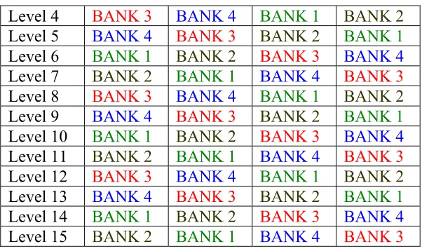
Level 4 BANK 3 BANK 4 BANK 1 BANK 2 Level 5 BANK 4 BANK 3 BANK 2 BANK 1 Level 6 BANK 1 BANK 2 BANK 3 BANK 4 Level 7 BANK 2 BANK 1 BANK 4 BANK 3 Level 8 BANK 3 BANK 4 BANK 1 BANK 2 Level 9 BANK 4 BANK 3 BANK 2 BANK 1 Level 10 BANK 1 BANK 2 BANK 3 BANK 4 Level 11 BANK 2 BANK 1 BANK 4 BANK 3 Level 12 BANK 3 BANK 4 BANK 1 BANK 2 Level 13 BANK 4 BANK 3 BANK 2 BANK 1 Level 14 BANK 1 BANK 2 BANK 3 BANK 4 Level 15 BANK 2 BANK 1 BANK 4 BANK 3
Table 3-1: Memory mapping for scheme 1
Figure 3-1: Memory bank mapping for binary tree
The following table shows the number of entries in each bank at every level. Level of Tree No. of entries / Bank En
1 0 2 0 3 0 4 0 5 4 4 6 8 12 7 16 28 8 32 60 9 64 124
Table 3-2 Cumulative entries at each level
The next level row and column number required for DRAM access can be calculated as follows:
Cn+1 = (Cn * 2) - 1(d)
Rn+1 = [ En + (Cn - 1) * 2] / 64 Actual column number = Cn * 4
Where:
Cn : column number at level n Rn : Row number at level n
En : Cumulative sum of all the entries till the current level in 1 bank.
d : This is either 0 or 1 depending on the result of comparison during the binary search at level n.
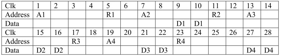
The signals for the memory are generated in the following sequence:
Clk 1 2 3 4 5 6 7 8 9 10 11 12 13 14
Address A1 R1 A2 R2 A3
Data D1 D1
Clk 15 16 17 18 19 20 21 22 23 24 25 26 27 28
Address R3 A4 R4
Data D2 D2 D3 D3 D4 D4
Table 3-3 Memory signals for Scheme 1
From the above description it is clear that we can access 128 bits every 6 clock cycles. The operating frequency of the memory is 250MHz (4ns – time period)
A million entry routing table requires 21 accesses to complete the binary search in the worst case. The first 4 accesses are in the SRAM, hence 17 DRAM accesses are required.
Total DRAM access time = 17 * 24 ns = 408 ns
For accomplishing 1.5 million lookups per second, we have 666ns per packet. Slack time = 666 – 408 = 258ns
In this 258ns we have to do lookup for the first 4 levels in the SRAM and at the end of the search access the Path information field and the next hop address. These operations can be performed in parallel with the DRAM access for another packet since all this data is on a separate memory chip.
This scheme meets our criteria of 1.5 million lookups per second. However in this scheme pipelining is not possible because for each packet we need to access all the memory banks. The memory efficiency is 33%.
3.3 Scheme 2
half of the binary tree the levels are alternately stored in the two available banks. The final memory layout looks like the following table:
Level 1 BANK 1 Level 2 BANK 2
Level 3 BANK 1 Level 4 BANK 2
Level 5 BANK 1 Level 6 BANK 2
Level 7 BANK 3 Level 8 BANK 4
Level 9 BANK 3 Level 10 BANK 4
Level 11 BANK 3 Level 12 BANK 4
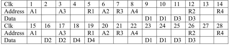
Table 3-4 Memory layout for Scheme 2 The memory access pattern is as follows :
Clk 1 2 3 4 5 6 7 8 9 10 11 12 13 14
Address A1 A3 R1 A2 R3 A4 R2 R4
Data D1 D1 D3 D3
Clk 15 16 17 18 19 20 21 22 23 24 25 26 27 28
Address A1 A3 R1 A2 R3 A4 R2 R4
Data D2 D2 D4 D4 D1 D1 D3 D3
Table 3-5 Memory signals for Scheme 2
From Table 3-5 it is clear that we can access 128 bits every 3.5 clock cycles. The operating frequency of the memory is 250MHz (4ns – time period). Hence it requires 3.5 * 4 = 14ns for each DRAM access.
A million entry routing table requires 21 accesses to complete the binary search in the worst case. If the first 4 accesses are in the SRAM, hence 17 DRAM accesses are required.
In this scheme all the accesses for the binary search can be done to the DRAM and hence in the worst case 21 DRAM accesses would be required. 17 DRAM accesses are used only for comparison with the other scheme. 1 lookup takes 238 ns, hence we can do 4.2 million lookups per second. We achieve a memory efficiency of 57% with this scheme.
3.4 Scheme 3
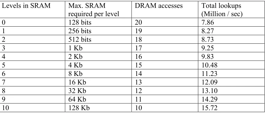
This scheme is a modification of Scheme 2 to get optimum performance from Reduced Latency DRAM (RLDRAM; MT49H8M32 from Infineon & Micron). This method will pipeline 4 lookups at a time so that memory efficiency reaches 100 %. The RLDRAM has 8 banks and hence the binary tree can be divided into 4 equal parts horizontally and each portion is stored in 2 banks.
Levels in SRAM Max. SRAM
required per level DRAM accesses Total lookups (Million / sec)
0 128 bits 20 7.86
1 256 bits 19 8.27
2 512 bits 18 8.73
3 1 Kb 17 9.25
4 2 Kb 16 9.83
5 4 Kb 15 10.48
6 8 Kb 14 11.23
7 16 Kb 13 12.09
8 32 Kb 12 13.10
9 64 Kb 11 14.29
10 128 Kb 10 15.72
Table 3-6 Lookup rate for Scheme 3
The above table is calculated on the basis of the following assumptions: 1. The lookup rate is based entirely on the DRAM access time.
2. Since SRAM data, final Path Information field and port address are stored outside the RLDRAM, those lookups can be performed in parallel and hence have no impact on the lookup speed.
Chapter 4 Trie based lookup and update scheme
4.1 Introduction
New DRAM [17] memory chips are available which can perform a random access every 25ns. This gives a lookup rate of 40 million lookups per second, much higher than that required by an OC-192c link. There has been a steady increase in the SRAM available in a SoC solution, LSI Logic[16] can provide 100 Mb of SRAM and 64 million logic gates on a single chip.
We have described the available state-of-the art technologies and our trie based scheme. A brief discussion of issues arising in the implementation of the trie based scheme for million entry IPv6 tables is given with respect to two example requirements. We first take a conservative requirement of 1.5 million lookups per second and then look at the more challenging OC-192c lookup rate.
4.2 1.5 million lookups per second
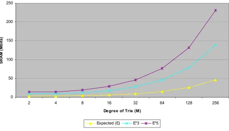
following charts plot the variation of SRAM requirement and trie depth with respect to the degree of the trie.
From Figure 4-2 we observe that a trie of degree greater than 64 would require more than 100 Mbits of SRAM giving us a good indication that degree of trie should be less than 64.
The following two charts can be used for making trade-offs between SRAM requirement and hardware requirement.
Depth v/s Degree of Trie
0 20 40 60 80 100 120 140
2 4 8 16 32 64 128 256
Degree (M)
De
p
th
(
D
)
Depth (D)
SRAM Requirement
0 50 100 150 200 250
2 4 8 16 32 64 128 256
Degree of Trie (M)
S
R
A
M
(M
b
its
)
Expected (E) E*3 E*5
Figure 4-2 SRAM requirement for trie
Suppose we take a 16 degree trie then the memory requirements are as follows: SRAM = 6Mbit * 3 = 18 Mbit
DRAM = 18 Mbit * 8 = 144 Mbit
The expected SRAM for a 16 degree trie is 5.77 bits per entry, hence approximately 6Mbits for a million entry table. A multiplication factor of 3 is used to provide sufficient space for actual routing tables. Assuming 8bits for storing port numbers, we get the DRAM requirement as 144Mbit.
easily searched in 20.8ns. This implementation can be done using off the shelf FPGA [18] and SRAM [19] chips.
This implementation requires no pipelining and hence the hardware is reduced. The SRAM and DRAM requirements are also feasible.
4.3 Update Architecture with 25ns DRAM
We believe that update performance will become an important parameter for lookup schemes in the near future when IPv6 is deployed and size of routing tables will increase to have million entries. The move to IPv6 will make it difficult for indexing schemes like [5] to scale and would also make trie based schemes to take longer. The increase in the routing table sizes will have an impact on the binary search based schemes. We show that the scheme presented in [6] is especially suitable for large IPv6 tables and we use it to explain the update architecture.
The past lookup schemes have used algorithmic techniques to show the update performance or show it by experiments. We develop an architecture and bound the worst case update performance.
0.0.0.1
| Space 1
|
100.255.255.255
--- 101.0.0.0
| Space 2
|
200.255.255.255
--- 201.255.255.255
| Space 3
|
255.255.255.254
without affecting the lookup performance, an important requirement is to keep prefixes in only 1 address space.
Analysis of the prefix distribution of IP addresses as presented in Figure 4-3 and Figure 4-4.
We observe that there are no prefixes smaller than 8 significant bits, hence dividing the address space at a boundary decided by an 8 bit prefix will remove the problem of one prefix existing in multiple address spaces. This solution does not increase the number of prefixes since no prefix is expanded as done in [5].
We provide the performance results for our scheme for the most demanding routing tables and these exceed the requirements of current routing tables. As a sample implementation we consider a million entry IPv6 routing table. According to the trie based scheme described in [6], it would require 18Mbits of on-chip SRAM. If we divide the address space into 3 spaces then we need 6Mbits for each address space. We consider a 80bit 300MHz DDR bus to write the SRAM. This gives us an effective bandwidth of 48Gbps and requires 125us to write 6Mbits of SRAM. Hence we can do 8000 updates per second in the worst case with no impact on the lookup performance.
4.3.1 Implementation
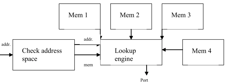
Figure 4-5 Top level view
addr.
Lookup engine Check address
space
Mem 1 Mem 2 Mem 3
Mem 4
addr.
mem
The top level view of the hardware is given in Figure 4-5. The “check address space” module has simple comparators to decide the address space in which the IP address should be searched. The information about the memory to be used is passed to the lookup engine along with the IP address. The lookup engine has a 32 stage pipeline to decide the DRAM address. The Mem1, Mem2, Mem3 and Mem4 are the on-chip SRAM modules. Each SRAM module is 6Mbit.
Figure 4-6 Lookup Engine
4.3.1.1 SRAM Access
The SRAM access module is used to latch the data coming out from the SRAM. It holds the data for 4 clock cycles.
4.3.1.2 Mask Generator
The bit-extractor takes the 4 bits of the 128-bit address depending on the level, which is traversed. For e.g.: first 4 bits for level0, the next four for level 1 & so on. These 4 bits are appended with the 2-bit column pointer to give the 6-bit final offset. It also outputs the current 4-bit offset from the IP address to the sum of ones block to set the Column number in case a ‘0’ is found in a particular level.
To determine the sum of ones till a certain bit position we generate a 64 bit mask to remove the unwanted bits from the SRAM row. The offset that is generated from the bit extractor is used to determine how many bits in the mask need to be set to 1 while all the other bits are set to 0. If for example the offset were 8, then the output of the mask
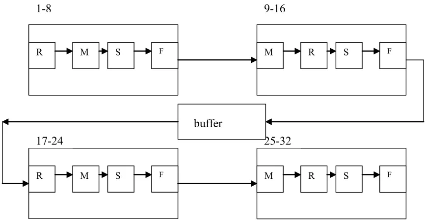
1-8 9-16
R M S F M R S F
R M S F M R S F
17-24 25-32
generator would be 00000000000000ff. The 64-bit output of the mask generator goes to the input of sum of one’s where it is ANDed with the current SRAM row.
4.3.1.3 Sum of 1’s
The sum of ones is basically composed of a compressor and adders as shown in Figure 4-7. The sum of ones input is the ANDing of the mask and the SRAM row and it gives the 7 bit sum of ones as the output.
Figure 4-7 Sum 0f 1’s
4.3.1.4 Final stage logic
Along with the sum of 1’s as per the mask generator output, the logic to decide whether to traverse to the next level was also implemented in this block. It checks the respective SRAM bit for 1 or 0 and increments the level pointer accordingly. If it finds a 0, it calculates the DRAM row number for the next hop and sets the column number as
4:3 Compressor (18)
3 bit Adder (9)
4 bit Adder (4)
5 bit Adder (1)
6 bit Adder (1)
Chapter 5 Verification
Analytical verification is done for the memory mapping of binary search scheme. We feel the idea is developed in sufficient detail to get performance estimates for the binary search scheme.
We present a solution for the trie based scheme for doing 1.5 million lookups per second. This solution is based on a previous implementation to get timing estimates.
The trie based scheme for performing fast update and lookup every 25ns was implemented in Verilog. Simulations were done to verify the correctness. The sample routing tables used had 3-4 entries per address space and the SRAM related to one of the address spaces was changed during simulation and the new SRAM was used to check the update mechanism. All the modules were synthesized in Synopsys except for the SRAM. The first stage of the pipeline with inputs and outputs is shown in Figure 5-1.
Chapter 6 Conclusion and Future Work
We evaluated 2 IP lookup schemes with respect to scalability with increasing IP address size and increase in the routing table size. The trie based scheme scales better than the binary search scheme because it requires only one DRAM access. The binary search scheme has no impact due to the larger address size but the large routing table size degrades the performance. The binary search scheme could achieve a maximum of 15.72 Million lookups/ sec. by using 100% of the DRAM memory bandwidth. The trie based scheme is dependent on only the DRAM access time. Deeper pipelining of the trie based scheme helps to keep up with the smaller DRAM cycle times. We also observed that deeper pipelining also requires higher SRAM bandwidth and this could be a limiting factor. If the SRAM bandwidth cannot be achieved then we can partition the trie levels into different SRAM to increase the SRAM bandwidth. However the drawback is that we need to provide more SRAM.
We have proposed a generic architecture to have good update performance for lookup schemes without sacrifising the lookup rate. We bound the worst case performance irrespective of the lookup scheme and do not depend on the average case performance which could lead to packet losses. This architecture can be scaled to provide higher update rates by using higher number of address spaces. This increase in the number of address spaces increases the number of on-chip data buses and could be a limiting factor.
6.1 Future Work
mapping the sparse last level in a more efficient manner. New memory architectures can be analyzed with respect to better memory bandwidth utilization.
Bibliography
[1]Ruiz-Sanchez, M.A.; Biersack, E.W.; Dabbous, W., Survey and taxonomy of IP address lookup algorithms, IEEE Network April 2001
[2]M. Waldvogel, G. Varghese, J. Turner, and B. Plattner, Scalable High Speed IP Routing Lookups, Proc. ACM SIGCOMM 97, Sept. 1997, pp. 25 36.
[3]David E. Taylor, John W. Lockwood, Todd S. Sproull, Jonathan S. Turner, David B. Parlour, Scalable IP Lookup for Programmable Routers, IEEE Infocom 2002, New York NY, June 23-27, 2002
[4]B. Lampson, V. Srinivasan, and G. Varghese, IP Lookups Using Multiway and Multicolumn Search, Proc. IEEE INFOCOM 98, Apr. 1998, pp. 1248 56. 25
[5]Pankaj Gupta, Steven Lin, and Nick McKeown, Routing lookups in hardware at memory access speeds, in IEEE Infocom, 1998.
[6]P. Mehortra, P. Franzon, Novel Hardware Implementation for Fast Address Lookups, 2002 Workshop on High Performance Switching and Routing
[7]Marcel Waldvogel, George Varghese, Jon Turner, Bernhard Plattner; Scalable High-Speed Prefix Matching, ACM Transactions on Computer Systems 2001
[8]Pronita Mehrotra, “Memory Intensive Architectures for DSP and Data Communication”, Ph.D Dissertation, NCSU, 2002
[9]P. Mehortra, P. Franzon, “Binary Search Schemes for Fast IP Lookups,” IEEE Globecom, November, 2002
[10]Hinden, R., Deering S.; RFC 2373 - IP Version 6 Addressing Architecture [11]Rasanen, Asko; IPv6 and 3G/UMTS mobile Core Networks;
http://www.ipv6forum.com/navbar/events/birmingham00/presentations/PDF/AskoRa sanen.pdf
[12]http://www.internetworking.hitachi.com/docs/IPv6_datasheet.pdf [13]Metro Edge Router test, http://www.lightreading.com;
http://www.lightreading.com/document.aspsite=testing&doc_id=25454&page_numbe r=1
[14]IBM Embedded SRAM; http
://www-3.ibm.com/chips/products/asics/products/sramselguide.pdf
[15] Michigan University and Merit Network. Internet Performance Management and Analysis (IPMA) Project. (http://www.merit.edu/ipma)
[16]LSI Logic’s G90 SoC Solution,
www.lsilogic.com/techlib/marketing_docs/asic/g90PB.pdf [17] RLDRAM, http://www.rldram.com
Appendix
A1: Code
module level_1(clock20, eval_in, lprev_control, lprev_row, lprev_col, lip_address, lsram_raw_data, lcontrol, lrow, lcolumn,
shift_ip_address);
// This module makes all the wire connections for 1 stage of the // pipeline
input clock20; input eval_in;
input lprev_control; input [14:0] lprev_row; input [5:0] lprev_col; input [127:0] lip_address; input [79:0] lsram_raw_data; output lcontrol;
output [14:0] lrow; output [5:0] lcolumn;
output [127:0] shift_ip_address;
wire [15:0] lsum_16_1,lsum_16_2; wire [63:0] ldata_64_1,ldata_64_2; wire [6:0] lsumof1s_7_1;
wire [62:0] ldata_63_1,lmask_63_1; wire [14:0] lrow_10_1;
wire [5:0] lcolumn_6_1; wire [1:0] lcolumn_2_1; wire lcontrol_1;
wire [31:0] ip_addr_3to5;
wire eval1, eval2, eval3,eval4;
assign ldata_63_1 = ldata_64_1[63:1]; assign lcolumn_2_1 = lprev_col[5:4];
assign lcontrol_1 = lprev_control; assign lrow_10_1 = lprev_row; assign lcolumn_6_1 = lprev_col; assign lsum_16_2 = lsum_16_1; assign ldata_64_2 = ldata_64_1;
sram_access access1(clock20, eval_in, lsram_raw_data, lsum_16_1,ldata_64_1,eval1);
mask mask1( clock20, eval1, lcolumn_2_1, lip_address[127:124], lmask_63_1, eval2);
sum_of1 sum1(clock20,eval2, ldata_63_1, lmask_63_1, lsumof1s_7_1, eval3);
module mask( clock20, eval_in, prev_column, curr_ip, mask_64_bit,eval_out);
input clock20; // System clock20 input eval_in; // Evaluation trigger
input [1:0] prev_column; // Column number higher order bits from previous stage
input [3:0] curr_ip; // 4 bits of IP Address for current stage
output [62:0] mask_64_bit; // 64 bit mask for data of current stage output eval_out; reg[62:0] mask_64_bit; reg[15:0] mask_16_bit; reg eval_out;
reg [15:0] mask1, mask2, mask3, mask4; // partial mask bits
always @(curr_ip)
casex({curr_ip[3],curr_ip[2], curr_ip[1], curr_ip[0]}) // synopsys full_case parallel_case
4'b0000:
mask_16_bit = 16'b0000000000000000; 4'b0001:
mask_16_bit = 16'b1000000000000000; 4'b0010:
mask_16_bit = 16'b1100000000000000; 4'b0011:
mask_16_bit = 16'b1110000000000000; 4'b0100:
mask_16_bit = 16'b1111000000000000; 4'b0101:
mask_16_bit = 16'b1111100000000000; 4'b0110:
mask_16_bit = 16'b1111110000000000; 4'b0111:
mask_16_bit = 16'b1111111000000000; 4'b1000:
mask_16_bit = 16'b1111111100000000; 4'b1001:
mask_16_bit = 16'b1111111110000000; 4'b1010:
mask_16_bit = 16'b1111111111000000; 4'b1011:
mask_16_bit = 16'b1111111111100000; 4'b1100:
mask_16_bit = 16'b1111111111110000; 4'b1101:
mask_16_bit = 16'b1111111111111000; 4'b1110:
mask_16_bit = 16'b1111111111111100; 4'b1111:
mask_16_bit = 16'b1111111111111110; endcase
casex({prev_column[1], prev_column[0]}) // synopsys full_case parallel_case
2'b00: begin
mask1 <= mask_16_bit; mask2 <= 16'b0;
mask3 <= 16'b0; mask4 <= 16'b0; end
2'b01: begin
mask1 <= 16'hffff; mask2 <= mask_16_bit; mask3 <= 16'b0;
mask4 <= 16'b0; end
2'b10: begin
mask1 <= 16'hffff; mask2 <= 16'hffff; mask3 <= mask_16_bit; mask4 <= 16'b0;
end 2'b11: begin
mask1 <= 16'hffff; mask2 <= 16'hffff; mask3 <= 16'hffff; mask4 <= mask_16_bit; end
endcase end
always @(posedge clock20) begin
if(eval_in)
mask_64_bit <= {mask1,mask2,mask3,mask4[15:1]}; else
mask_64_bit <= mask_64_bit; end
always @(posedge clock20) begin
eval_out = eval_in; end
endmodule
module module5_1(clock20, eval_in, prev_control_2, sram_data_1, sram_sum_1, sumof1_2, prev_row_2, prev_col_2, ip_address, control_3, row_3, col_3,shift_ip_addr_3, eval_out);
input prev_control_2; input [63:0] sram_data_1; input [15:0] sram_sum_1; input [6:0] sumof1_2; input [14:0] prev_row_2; input [5:0] prev_col_2; input [127:0] ip_address; output control_3;
output [14:0] row_3; output [5:0] col_3;
output [127:0] shift_ip_addr_3; output eval_out;
reg control_3; reg [14:0] row_3; reg [5:0] col_3;
reg [127:0] shift_ip_addr_3; reg eval_out;
reg control; reg [14:0] row; reg [5:0] col;
wire [15:0] total_row, new_row; wire [0:63] sram_data_1_twist; wire [5:0] col_for_control;
assign sram_data_1_twist = sram_data_1;
assign col_for_control = {prev_col_2[5:4], ip_address[127:124]};
assign total_row = sumof1_2 + sram_sum_1 + 1'b1; assign new_row = total_row >> 2;
always @(new_row or prev_control_2 or prev_row_2 or control) begin
if(prev_control_2 == 1'b0 | control == 1'b0)
row <= prev_row_2;
else
row <= {prev_row_2[14:13],new_row};
end
always @(posedge clock20) if(eval_in)
row_3 = row; else
row_3 = row_3;
always @(total_row or ip_address or prev_control_2 or prev_col_2 or control or col_for_control)
begin
if(prev_control_2 == 1'b0 | control == 1'b0) if( prev_control_2 == 1'b0)
col <= prev_col_2;
else
end
always @(posedge clock20) if(eval_in)
col_3 = col; else
col_3 = col_3;
always @(prev_control_2 or prev_col_2 or sram_data_1_twist or col_for_control )
begin
if(prev_control_2 == 1'b0 )
control <= 1'b0;
else
control <= sram_data_1_twist[col_for_control]; end
always @(posedge clock20) if(eval_in)
control_3 = control; else
control_3 = control_3;
always @(posedge clock20) if(eval_in)
shift_ip_addr_3 = ip_address; else
shift_ip_addr_3= shift_ip_addr_3;
always @(posedge clock20) eval_out = eval_in;
endmodule
module sram_access(clock20, eval_in, tpr_data, sram_sum,sram_data, eval_out);
parameter sram_addr_lines = 13; parameter sram_data_lines = 64; parameter sram_sum_lines = 16;
input clock20; input eval_in;
input [sram_data_lines + sram_sum_lines -1 : 0] tpr_data; output[sram_sum_lines - 1 : 0] sram_sum;
output [sram_data_lines - 1 : 0] sram_data; output eval_out;
reg [sram_sum_lines - 1 : 0] sram_sum; reg [sram_data_lines - 1 : 0] sram_data; reg eval_out;
always @(posedge clock20) begin
if(eval_in) begin
end else begin
sram_data <= sram_data; sram_sum <= sram_sum; end
end
always @(posedge clock20) eval_out = eval_in;
endmodule
module sum_of1(clock20,eval_in, sram_data_1, mask_1, sum_of1_2,eval_out);
input clock20; input eval_in;
input [62:0] sram_data_1; input [62:0] mask_1; output [6:0] sum_of1_2; output eval_out;
reg [6:0] sum_of1_2; reg eval_out;
wire [1:0] sum1_1,
sum1_2,sum1_3,sum1_4,sum1_5,sum1_6,sum1_7,sum1_8,sum1_9,sum1_10,sum1_11 ,sum1_12,sum1_13,sum1_14,sum1_15,sum1_16,sum1_17,sum1_18,sum1_19,sum1_2 0,sum1_21,sum1_22,sum1_23,sum1_24,sum1_25,sum1_26,sum1_27; wire [2:0] sum2_1,sum2_2,sum2_3,sum2_4,sum2_5,sum2_6,sum2_7,sum2_8,sum2_9,sum2_10, sum2_11,sum2_12,sum2_13,sum2_14,sum2_15,sum2_16,sum2_17,sum2_18; wire [2:0] sum3_1,sum3_2,sum3_3,sum3_4,sum3_5,sum3_6,sum3_7,sum3_8,sum3_9;
wire [3:0] sum4_1, sum4_2,sum4_3,sum4_4;
wire [4:0] sum5_1; wire [5:0] sum5_2; wire [6:0] sum6_1; wire [6:0] sum7_1; wire [62:0] and_out;
assign and_out = mask_1 & sram_data_1;
/* Start of 7:3 compressor */
assign sum3_1 = sum2_1 + sum2_2 ;
assign sum1_4 = and_out[7] + and_out[8] ; assign sum1_5 = and_out[9] + and_out[10] ; assign sum1_6 = and_out[11] + and_out[12] ; assign sum2_3 = sum1_4 + sum1_5;
assign sum2_4 = sum1_6 + and_out[13]; assign sum3_2 = sum2_3 + sum2_4 ;
assign sum1_7 = and_out[14] + and_out[15] ; assign sum1_8 = and_out[16] + and_out[17] ; assign sum1_9 = and_out[18] + and_out[19] ; assign sum2_5 = sum1_7 + sum1_8;
assign sum2_6 = sum1_9 + and_out[20]; assign sum3_3 = sum2_5 + sum2_6 ;
assign sum1_10 = and_out[21] + and_out[22] ; assign sum1_11 = and_out[23] + and_out[24] ; assign sum1_12 = and_out[25] + and_out[26] ; assign sum2_7 = sum1_10 + sum1_11;
assign sum2_8 = sum1_12 + and_out[27]; assign sum3_4 = sum2_7 + sum2_8 ;
assign sum1_13 = and_out[28] + and_out[29] ; assign sum1_14 = and_out[30] + and_out[31] ; assign sum1_15 = and_out[32] + and_out[33] ; assign sum2_9 = sum1_13 + sum1_14;
assign sum2_10 = sum1_15 + and_out[34]; assign sum3_5 = sum2_9 + sum2_10 ;
assign sum1_16 = and_out[35] + and_out[36] ; assign sum1_17 = and_out[37] + and_out[38] ; assign sum1_18 = and_out[39] + and_out[40] ; assign sum2_11 = sum1_16 + sum1_17;
assign sum2_12 = sum1_18 + and_out[41]; assign sum3_6 = sum2_11 + sum2_12 ;
assign sum1_19 = and_out[42] + and_out[43] ; assign sum1_20 = and_out[44] + and_out[45] ; assign sum1_21 = and_out[46] + and_out[47] ; assign sum2_13 = sum1_19 + sum1_20;
assign sum2_14 = sum1_21 + and_out[48]; assign sum3_7 = sum2_13 + sum2_14 ;
assign sum1_22 = and_out[49] + and_out[50] ; assign sum1_23 = and_out[51] + and_out[52] ; assign sum1_24 = and_out[53] + and_out[54] ; assign sum2_15 = sum1_22 + sum1_23;
assign sum2_16 = sum1_24 + and_out[55]; assign sum3_8 = sum2_15 + sum2_16 ;
assign sum3_9 = sum2_17 + sum2_18 ;
/* End of 7:3 compressor */
/* 3 bit adders */
assign sum4_1 = sum3_1 + sum3_2; assign sum4_2 = sum3_3 + sum3_4; assign sum4_3 = sum3_5 + sum3_6; assign sum4_4 = sum3_7 + sum3_8;
/* 4 bit adders */
assign sum5_1 = sum4_1 + sum4_2 ;
assign sum5_2 = sum4_3 + sum4_4 + sum3_9;
/* 5 bit adder */
assign sum6_1 = sum5_1 + sum5_2 ;
/* 6 bit adder */
assign sum7_1 = sum6_1 ;
// assign sum7_1 = sum6_1 + sum3_9;
always @(posedge clock20) if(eval_in)
sum_of1_2 <= sum7_1; else
sum_of1_2 <= sum_of1_2;
always @(posedge clock20) eval_out = eval_in; endmodule
module buffer(clock20, lprev_control, lprev_row, lprev_col, lip_address, lcontrol, lrow, lcolumn, shift_ip_address);
input clock20;
input lprev_control; input [14:0] lprev_row; input [5:0] lprev_col; input [127:0] lip_address; output lcontrol;
output [14:0] lrow; output [5:0] lcolumn;
output [127:0] shift_ip_address;
reg lcontrol; reg [14:0] lrow; reg [5:0] lcolumn;
reg [127:0] shift_ip_address;
reg [127:0] shift_ip_address1;
always @(posedge clock20) begin
lcontrol1 = lprev_control; lrow1 = lprev_row;
lcolumn1 = lprev_col;
shift_ip_address1 = lip_address; end
always @(posedge clock20) begin
lcontrol = lcontrol1; lrow = lrow1;
lcolumn = lcolumn1;
shift_ip_address = shift_ip_address1; end
A2: Script
TOPLEVEL = asic_logic TECH = ncsulib25 CLK = clock20 RST = reset
CLK_PERIOD = 6750 MAX_AREA = 0
DO_UNGROUP = no /* yes, no */ DO_VERIFY = no /* yes, no */ CLK_UNCERTAINTY = 100 /* 100 ps */
DFF_CKQ = 200 /* Clk to Q in technology time units */ DFF_SETUP = 100 /* Setup time in technology time units */
read -f verilog asic_logic_eval.v current_design TOPLEVEL
link uniquify
check_design
DFF_CELL = dp_2
LIB_DFF_D = ncsulib25/dp_2/ip OPER_COND = slow
/* Clocks constraints */
create_clock clock20 -period CLK_PERIOD set_fix_hold CLK
set_clock_skew all_clocks() -uncertainty CLK_UNCERTAINTY set_dont_touch_network all_clocks()
/* Reset constraints */ set_driving_cell -none RST set_drive 0 RST
set_dont_touch_network RST
/* All inputs except reset and clock */
all_inputs_wo_rst_clk = all_inputs() - CLK - RST
/* Set output delays and load for output signals *
* All outputs are assumed to go directly into * external flip-flops for the purpose of this * synthesis
*/
set_output_delay DFF_SETUP -clock CLK all_outputs() set_load load_of(LIB_DFF_D) * 4 all_outputs()
/* Input delay and driving cell of all inputs *
* All these signals are assumed to come directly from * flip-flops for the purpose of this synthesis
* */
set_ultra_optimization -f
compile_new_optimization = true
current_design TOPLEVEL
characterize -constraints {level1} current_design = level_1
compile -boundary_optimization -map_effort medium report_timing
current_design TOPLEVEL
characterize -constraints {level2} current_design = level_2
compile -boundary_optimization -map_effort medium -ungroup_all
current_design TOPLEVEL
characterize -constraints {level3} current_design = level_3
compile -boundary_optimization -map_effort medium
current_design TOPLEVEL
characterize -constraints {level4} current_design = level_4
compile -boundary_optimization -map_effort medium
current_design TOPLEVEL
characterize -constraints {level5} current_design = level_5
compile -boundary_optimization -map_effort medium
current_design TOPLEVEL
characterize -constraints {level6} current_design = level_6
compile -boundary_optimization -map_effort medium
current_design TOPLEVEL
characterize -constraints {level7} current_design = level_7
compile -boundary_optimization -map_effort medium
current_design TOPLEVEL
characterize -constraints {level8} current_design = level_8
compile -boundary_optimization -map_effort medium
current_design TOPLEVEL
characterize -constraints {level9} current_design = level_9
compile -boundary_optimization -map_effort medium
current_design TOPLEVEL
characterize -constraints {level10} current_design = level_10
compile -boundary_optimization -map_effort medium
current_design TOPLEVEL
compile -boundary_optimization -map_effort medium
current_design TOPLEVEL
characterize -constraints {level12} current_design = level_12
compile -boundary_optimization -map_effort medium
current_design TOPLEVEL
characterize -constraints {level13} current_design = level_13
compile -boundary_optimization -map_effort medium
current_design TOPLEVEL
characterize -constraints {level14} current_design = level_14
compile -boundary_optimization -map_effort medium
current_design TOPLEVEL
characterize -constraints {level15} current_design = level_1
compile -boundary_optimization -map_effort medium
current_design TOPLEVEL
characterize -constraints {level16} current_design = level_16
compile -boundary_optimization -map_effort medium
current_design TOPLEVEL
characterize -constraints {level17} current_design = level_17
compile -boundary_optimization -map_effort medium
current_design TOPLEVEL
characterize -constraints {level18} current_design = level_18
compile -boundary_optimization -map_effort medium
current_design TOPLEVEL
characterize -constraints {level19} current_design = level_19
compile -boundary_optimization -map_effort medium
current_design TOPLEVEL
characterize -constraints {level20} current_design = level_20
compile -boundary_optimization -map_effort medium
current_design TOPLEVEL
characterize -constraints {level21} current_design = level_21
compile -boundary_optimization -map_effort medium
current_design TOPLEVEL
current_design TOPLEVEL
characterize -constraints {level23} current_design = level_23
compile -boundary_optimization -map_effort medium
current_design TOPLEVEL
characterize -constraints {level24} current_design = level_24
compile -boundary_optimization -map_effort medium
current_design TOPLEVEL
characterize -constraints {level25} current_design = level_25
compile -boundary_optimization -map_effort medium
current_design TOPLEVEL
characterize -constraints {level26} current_design = level_26
compile -boundary_optimization -map_effort medium
current_design TOPLEVEL
characterize -constraints {level27} current_design = level_27
compile -boundary_optimization -map_effort medium
current_design TOPLEVEL
characterize -constraints {level28} current_design = level_28
compile -boundary_optimization -map_effort medium
current_design TOPLEVEL
characterize -constraints {level29} current_design = level_29
compile -boundary_optimization -map_effort medium
current_design TOPLEVEL
characterize -constraints {level30} current_design = level_30
compile -boundary_optimization -map_effort medium
current_design TOPLEVEL
characterize -constraints {level31} current_design = level_31
compile -boundary_optimization -map_effort medium
current_design TOPLEVEL
characterize -constraints {level32} current_design = level_32
compile -boundary_optimization -map_effort medium
current_design TOPLEVEL report_area
report_timing

![Figure 4-3 Prefix length distribution [7]](https://thumb-us.123doks.com/thumbv2/123dok_us/1467459.1179793/26.612.127.502.389.692/figure-prefix-length-distribution.webp)