International Journal of Emerging Technology and Advanced Engineering
Website: www.ijetae.com (ISSN 2250-2459, ISO 9001:2008 Certified Journal, Volume 6, Issue 2, February 2016)
146
Design and Analysis of Fin Field Effect Transistor with
Complex Semiconductor Material as SiGe
Mona Sachan
1, Kamal Prakash Pandey
2, Rakesh Kumar Singh
31,2,3
Department of Electronics and Communication, SIET, Allahabad, India
Abstract-- In this paper, it is analyzed SiGe based FinFET transistor that designed for high speed and low power operation system. The work is mainly focused on the performance enhancement of SiGe FinFET using Silvaco simulation tools. The measured threshold voltage is 0.498589 V for conventional SOI based FinFET and 0.0647597 V for purposed SiGe FinFET which is obtained by the simulation subthreshold voltage of SiGe FinFET is 0.56348 V/decade and 0.072853 V/decade for SOI FinFET. It is observed that the SiGe FinFET has lower threshold voltage than the higher subthreshold of conventional SOI FinFET. This leads to increase in channel drive current and reduced power consumption.
Keywords-- Silicon on Insulator FET, Depletion, FinFET.
I. INTRODUCTION
The idea of the field effect transistor has been known for many years. It has some of its earliest foundations in a
proposal made by Lilienfeld in 926, and to another paper by Heil in 1935 [1-5]. Then
during the 1940s Bell Laboratories set up a semiconductor research group. They investigated a number of areas pertaining to semiconductors and semiconductor technology, one of which was a device that would modulate the current flowing in a semiconductor channel by placing an electric field close to it. Field effect transistors are transistors which are made up of three regions, a Gate, Source, and Drain. Field Effect transistors have very high input impedance. This high input impedance causes them to have very little current run through them.
JFET is form of FET uses a reverse biased diode junction to provide the isolation from the channel. It is the most basic type of FET, and the one that was first developed. A JFET can be used as a voltage-controlled resistance or as an electronically-controlled switch. A p-type JFET consists of a channel of semiconductor material containing a large amount of positive charge carriers or holes, whereas an n-type JFET consists of a channel of semiconductor material containing a large amount of negative charge carriers or holes. At each end of the JFET, ohmic contacts form the source and drain. Electric charge flows through the channel between the source and drain. Electric current can be switched off by applying a reverse bias voltage to a gate. MOS FET or Insulated Gate FET is another form of FET uses an insulated layer between the gate and the channel.
Typically this is formed from a layer of oxide semiconductor. Here the gate is made of a layer of metal set down on the silicon oxide which in turn is on the silicon channel. The electric field of the gate extends through the dielectric and controls the resistance of the channel. In this device the input signal, which is applied to the gate, can increase the current through the channel. There are various types of MOSFET: CNTFET, MES FET, HEMT/PHEMT, Fin FET, VMOS, and Organic Field Transistor etc. Fin field effect transistor technology is now being used within integrated circuits to enable higher levels of integration to be achieved by allowing smaller feature sizes. This technology promises to provide the deliver superior levels of scalability needed to ensure that the current progress with increased levels of integration within integrated circuits can be maintained. The term FinFET was describing a non-planar, double-gate transistor built on an SOI substrate, based on the earlier single-gate transistor design [11-15]. The distinguishing characteristic of the FinFET is that the conducting channel is wrapped by a thin silicon "fin", which forms the body of the device. The thickness of the fin (measured in the direction from source to drain) determines the effective channel length of the device. The wrap-around gate structure provides a better electrical control over the channel and thus helps in reducing the leakage current and overcoming other short-channel effects. FinFET can also have two electrically independent gates, which gives circuit designers more flexibility to design with efficient, low-power gates. The most promising option is to create a vertical silicon ―fin‖ for the device of the channel.
II. STRUCTURE OF SOIFINFET
International Journal of Emerging Technology and Advanced Engineering
Website: www.ijetae.com (ISSN 2250-2459, ISO 9001:2008 Certified Journal, Volume 6, Issue 2, February 2016)
[image:2.612.49.299.129.358.2]147
Figure 1- Conventional SOI FinFETIn device simulation, both the SiGe FinFET and conventional SOI FinFET structure are simulated in simulation tools. The characteristic of the devices are also simulated to obtain the results of the SiGe FinFET and conventional SOI FinFET.
Device simulation is performed by ATLAS simulator to find the ID-VD characteristics of each device. For ID-VD
characteristic VD is varied from 0 to 1.6 V in each case.
These two devices simulated with the same condition to compare and observe electrical characteristics between them.
III. STRUCTURE OF SIGE FINFET
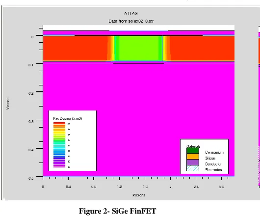
[image:2.612.324.589.130.351.2]The structure of Fin field effect transistor is designed as 2D structure of SiGe FinFET the conducting channel is wrapped by a thin silicon germanium fin, which forms the body of the device, all the parameters are same as designed the SOI Fin FET.
Figure 2- SiGe FinFET
FinFET is formed by deposition of Si layer of thickness 0.1µm on germanium layer with 0.4 µm. Finally, the structure of the SiGe FinFET is shown in the figure2. In this figure2 there is horizontally line which represent SiGe channel in FinFET.
IV. RESULT AND DISCUSSION
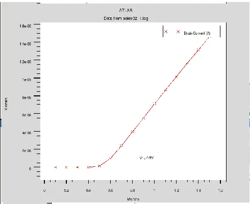
Figure 3- Sub Vt graph for SiGe FinFET
[image:2.612.325.580.432.626.2]International Journal of Emerging Technology and Advanced Engineering
Website: www.ijetae.com (ISSN 2250-2459, ISO 9001:2008 Certified Journal, Volume 6, Issue 2, February 2016)
[image:3.612.324.569.197.397.2]148
Figure3 is shows the variation in subthreshold voltages at 0.1 V drain voltage. This represent graph between drain current and drain voltage. The tony plot is obtained after the process simulation. The measured subthreshold voltage for FinFET is 0.56348 V/decade.Figure 4- Sub Vt graph for conventional SOI FinFET
[image:3.612.47.289.198.387.2]Figure 4 has shown the variation in subthreshold voltages at 0.1 V drain voltage. This represent graph between drain current and drain voltage. The tony plot is obtained after the process simulation. The measured subthreshold voltage is 0.072853 V/decade.
Figure 5- Threshold voltage for SiGe FinFET
Figure 5 has shown the ID-VG characteristics for SiGe
FinFET. This represent graph between drain current and gate voltage. The tony plot is obtained after the process simulation. The measured threshold voltage is 0.0647597 V.
Figure 6- Threshold voltage for conventional SOI FinFET
Figure 6 has shown the ID-VG characteristics for
conventional SOI FinFET. This represent graph between drain current and gate voltage. The tony plot is obtained after the process simulation. The measured threshold voltage is 0.498589 V. From comparison plot, it is observed that SiGe FinFET has lower threshold voltage than the conventional SOI FinFET which stated that SiGe FinFET has better performance than conventional SOI FinFET.
[image:3.612.48.295.464.645.2]International Journal of Emerging Technology and Advanced Engineering
Website: www.ijetae.com (ISSN 2250-2459, ISO 9001:2008 Certified Journal, Volume 6, Issue 2, February 2016)
149
Table1-Comparison of Electrical properties between SiGe and SOI based device
V. CONCLUSION
In this paper, it is described a SiGe FinFET transistor for high speed and low power consumption. The work has mainly focused on the performance enhancement. The measured threshold value is 0.498589 V for conventional SOI FinFET and the threshold value is 0.0647597 V for SiGe FinFET, it is obtained by device simulation. Subthreshold voltage for SiGe FinFET 0.56348 V/decade is better than the SOI FinFET as 0.072853 V/decade. Finally it s observed that SiGe FinFET has lower threshold voltage and higher subthreshold than the conventional SOI FinFET. This leads to an increase in channel drive current and also some reductions in power consumption.
REFERENCES
[1] B. Yu, L. Chang, S. Ahmed, H. Wang, S. Bell, and C.Y. Yang (2002), FinFET scaling to 10nm gate length. IEEE International Electron Devices Meeting, pages 251–253.
[2] B. Majkusiak, (1998) ―Semiconductor thickness effects in the double-gate SOI MOSFET,‖ IEEE Trans. Electron Devices, vol. 45, no. 5, pp. 1127–1134.
[3] Choi, Y.K. (2002) FinFET process refinements for improved mobility and gate work function engineering in IEEE International Electron Devices Meeting, Tech.
[4] Cartwright J (2011), Intel enters the third dimension, Nature, Doi: 10.1038/news, 274.
[5] C.-H. Lin (2012) ―Channel doping impact on FinFETs for 22 nm and beyond,‖ in Proc. Symp. Very Large Scale Integr. (VLSI) Technol, pp. 15-16.
[6] C. R. Manoj (2008) ―Device Design and Optimization Considerations for Bulk FinFETs‖ IEEE Transactions on Electron Devices, Vol. 55, no. 2.
[7] C. Auth (2012) ―A 22 nm high performance and low-power CMOS technology featuring fully-depleted tri-gate transistors, self-aligned contacts and high density MIM capacitors,‖ in Proc. IEEE Symp. Very Large Scale Integr. Syst. (VLSI) Technol, pp. 131–132. [8] D. Shamiryan, A. Redolfi, and W. Boullart (2009), Dry etching
process for bulk finfet manufacturing. Microelectronic Engineering archive, 86(1):96– 98.
[9] D. Hisamoto et.al. (2000) ―FinFET—A self-aligned double-gate MOSFET scalable beyond 20 nm,‖ IEEE Trans. Electron Devices, vol. 47, pp. 2320–2325.
[10] Dixit, A. Kottantharayil, N. Collaert, M. Goodwin, M. Jurczak, and K. de Meyer (2005), Analysis of the parasitic s/d resistance in multi- gate fets. IEEE Transactions on Electron De- vices, 52(6):1132– 1140.
Parameter
SiGe
SOI
Gate electrode
1.046e+00
01.954e+00(microns)
1.046e+00
01.954e+00(microns)
Substrate electrode
3e+00
3e+00
Doping concentration
1e17(p-type)
1e20(n-type)
1e17(p-type)
1e20(n-type)
Electric field
16
11.8
Energy band gap
0.663ev
1.08ev
Thermal velocities
Vn=1.56e+07(cm/s)
Vp=2.16e+07(cm/s)
Vn=1.08e+07(cm/s)
Vp=1.3e+07(cm/s)
Saturation velocities
1e+06(cm/s)
1.03e+07(cm/s)
Work function
4.170ev
4.170ev
Sub Vt
0.56348 v/decade
0.072853v/decade
Vt
0.0647597 v
0.498589 v
Dielectric constant
16
12
Electron mobility at 300
degree Kelvin
3800
1300
Hole mobility at 300 degree
Kelvin
International Journal of Emerging Technology and Advanced Engineering
Website: www.ijetae.com (ISSN 2250-2459, ISO 9001:2008 Certified Journal, Volume 6, Issue 2, February 2016)
150
[11] E. J. Nowak (2004) ―Turning silicon on its edge,‖ IEEE CircuitsDevices Mag., vol. 20, no. 1, pp. 20.
[12] F. Balestra, S. Cristoloveanu, M. Benachir, J. Brini, and T. Elewa (1987), Double-gate silicon-on- insulator transistor with volume inversion: A new device with greatly enhanced performance. IEEE Electron Devices Letters, 8(9):410–412.
[13] G.J. Hu, C. Chang, and Y.T. Chia (1987), Gate- voltage-dependent effective channel length and series resistance of ldd mosfets. IEEE Transac- tions on Electron Devices, 34:2469–2474.
[14] Huang, X. (1999), Sub 50-nm FinFET: PMOS International Electron Devices Meeting Technical Digest, p. 67. December 5–8. [15] Hisamoto, D. (1991), Impact of the vertical SOI 'Delta' Structure on