HEWLETT-PACKARD COMPANY RoseviUe Networks Division 8000 Foothills Boulevard Roseville, California 95678
HP 98623A
BCD Interface Card
FliPfj
HEWLETT
a:~ PACKARD
Installation Note
The Printing History below identifies the Edition of this Manual and any Updates that are included. Periodically, update packages are distributed which contain replacement pages to be merged into the manual, including an updated copy of this Printing History page. Also, the update may contain write-in instructions.
Each reprinting of this manual will incorporate all past updates; however, no new information will be added. Thus, the reprinted copy will be identical in content to prior printings of the same edition with the user-inserted update information. New editions of this manual will contain new information, as well as updates.
11
98623-90000
First Edition ... June 1981 Update 1 ... October 1984 Reprint (incorporating Update 1) ... October 1984
NOTICE
The information contained in this document is subject to change without notice.
HEWLETT-PACKARD MAKES NO WARRANTY OF ANY KIND WITH REGARD TO THIS MATERIAL, INCLUDING, BUT NOT LIMITED TO, THE IMPLIED WARRANTIES OF MERCHANTABILITY AND FITNESS FOR A PARTICULAR PURPOSE. Hewlett-Packard shall not be liable for errors contained herein or for incidental or consequential damages in connection with the furnishing, performance or use of this material.
This document contains proprietary information which is protected by copyright. All rights are reserved. No part of this document may be photocopied, reproduced or translated to another language without the prior written consent of Hewlett-Packard Company.
HP 98623
BCD Interface Card
Installation
The HP 98623A BCD Interface card is used to interface the HP 9826A to peripherals such as digital voltmeters and other devices whose output is in binary-coded decimal format. The cable optionally supplied with the interface has a connector at one end that is wired to match the in-terface. The other end of the cable is unterminated so that a connector can be attached that matches the equipment being connected to the computer.
Interface Card Installation
To install the interface, remove a blank cover from the left rear of the HP 9826A. Program the configuration switches as explained later, then plug the interface card into the LOWER slot in the available space. (The upper slot can be used for other non-liD options or for a DMA card.) Tighten the two retainer screws to hold the interface in place. Plug in the interface cable, and secure it with the two screws supplied, one on each side of the connector. The 3.5 mm by 10 mm screws (HP part number 0515-0067) have METRIC threads. Attempting to use non-metric screws causes thread damage. Plug the connector at the other end of the
interface cablel into the peripheral device. Installation is now complete.
Note
Do not touch the printed circuit connector fingers at the edge of the interface card. Fingerprints, skin oils, and other contamination can cause unreliable operation. To clean dirty connector fingers, use a cotton swab dampened in isopropyl alcohol. Be sure the fingers are completely clean and dry before installing the interface.
Configuring the Interface Card
Four clusters of configuration switches are provided as shown in Figure 1. They are
program-med as follows:
Setting the Select Code
Switch cluster Ul is used to program the interface select code. The switches are configured in a 5-bit binary format, with each bit having the following values:
Bit 0: 0 or 1 Bit 1: 0 or 2
Bit 2: 0 or 4 Bit 3: 0 or 8
Bit 4: 0 or 16
When each switch is set toward the rear of the computer (0 position) it has a value of zero. In
the forward setting (1 position), it takes on its non-zero value. The select code setting is the
sum of all non-zero values in the series. For example, to set the interface to select code 19, set
bits 0, l,and4totheir"I"positions(1
+
2+
16=
19).Setting the Interrupt Level
The interrupt level switch (U2) establishes the interrupt levels supplied to the computer. Set the switches to the required position as indicated in Figure 1, Table 4.
Setting the Peripheral Status Switches
The Peripheral Status Switch cluster (U24) is programmed as follows:
Option Format switch:
The Option Format switch selects between single- and dual-device BCD formats. The formats are shown in Figure 1, Table 5 (single device), and Figure 1, Tables 6 and 7 (dual devices).
Data Logic Sense switches:
The remaining Peripheral Status Switch settings program the logic sense of DATA, SIGN, and OVERLOAD signals. The ON position programs the logic sense to Positive True, Active High for a given line. Setting the switch OFF reverses the logic sense to Negative True, Active Low. Refer to Figure 1, Table 1 for a summary of the Peripheral Status Switch settings and func-tions.
Setting the Handshake Configuration
The Handshake Configuration Switch cluster (UI5) is used to program logic sense and signal type for each of the two Control and Flag lines. The signal lines and switch functions are as follows:
Function Mnemonic
DFLGA CTLA-2
EfLA
DFLGB CTLB-2 CTLBLogic Signal
Device Flag A Device Control A Device Control A Device Flag B Device Control B Device Control B
Switch Function
Flag logic sense from first BCD device. Control Bit timing, first BCD device. Control Bit logic sense, first BCD device. Flag logic sense from second BCD device. Control Bit timing, second BCD device. Control Bit logic sense, second BCD device.
Testing the Interface Card
Before you use the interface, or whenever you suspect an interface malfunction, you can use System Diagnostics software to determine that the interface is or is not functioning properly. To perform the diagnostic tests for the HP 98623A interface, remove the interface cable, then install a BCD interface test connector, that is ordered separately. HP part number 98623-67950.
Follow the instructions supplied with the diagnostics program to test the interface.
Service/Repair Procedures
The HP 98623A BCD Interface is not considered to be a field repairable item. Replacement cards can be ordered from your nearest HP Sales and Service office.
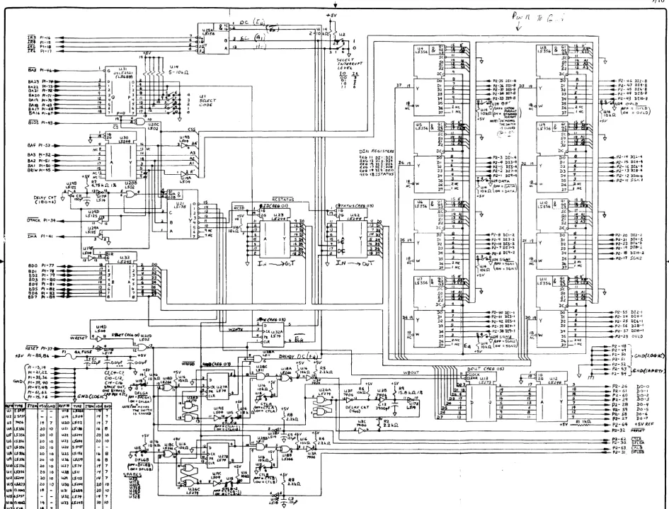
Theory of Operation
The interface contains the necessary circuitry to convert internal computer signals and exter-nal device sigexter-nals so that BCD devices can communicate with the computer. All communica-tion with the computer is through the edge connector opposite the cable connector. Signals include handshaking and data paths sufficient to control two BCD devices using a single interface. (The user is responsible for determining the necessary cable and connector figurations for adapting the unterminated cable to the one or two BCD devices being con-trolled. )
Data Format
Two data formats are available: standard and optional. The standard format, shown in Figure
1 Table 5, consists of a function code digit, a sign bit (SGNl), eight 4-bit BCD magnitude
digits, an exponent sign bit (SGN2), a 4-bit BCD exponent digit~ and an overload bit that
indicates whether the reading is valid or not. The optional format is shown in Figure 1, Tables
6 and 7. Note that no exponent digit is available because the highest bit of input digit 9 (019-8) is used as an overload bit for the second device. The exponent sign (SGN2) becomes the sign bit for the second device.
Output Data Lines
Eight output data bits (DOO-D07) are used to transmit commands and other information to the peripheral device. Data is latched and held until the next output operation. Actual func-tion depends on software implementafunc-tion in the I/O drivers of the computer operating system.
Preset
The Preset line is activated each time a computer system reset or an interface reset is
ex-ecuted. It is automatically activated when the computer power is turned on. The preset pulse
is active low, and lasts 15 microseconds. The handshake flip-flop, data output register, and
interrupt enable bit are reset at the same time.
Handshaking Lines
Data interchange between the interface and peripheral(s) is coordinated by the Control (CTLA and CTLB) and Device Flag (DFLGA and DFLGB) bits for devices A and B respec-tively.
Handshake timing is as follows:
• to: Interchange is inactive. Peripheral is ready for new command from Control Bit (CTLA/CTLB).
• t 1: Interface sends Control bit to peripheral device.
• t2: Peripheral changes flag from "ready" to "busy", indicating that the cornmand has been accepted.
• t3: Peripheral restores flag to "ready" state indicating the operation is complete. Flag "ready" usually implies valid data is available for input by the interface.
The following timing diagram shows the relationship between CONTROL and FLAG for each handshake configuration option as determined by the switch positions of U15. Timing applies to both A and B device handshake.
1
CTLA-2 or CTLB-2
ON (Type 2 Control)
...
, ----~--- CTLA or CTLB OFF
I~----~---
CTLAor CTLB ON1 1
1
---..--... ---.1
.... ___
DFLGA or DFLGB OFFData Flag ... , - - - -...
(DFLGA or DFLGB) ~
--"'--~----II'
CTLA-2 or CTLB-2
OFF (Type 1 Control)
Handshake Timing Diagram
DFLGA or DFLGB ON
CTLA or CTLB OFF
CTLA or CTLB ON
When the Control timing switch (CTLA-2/CTLB-2) is OFF (Type 1 timing), the control bit is cleared when the "device ready" (trailing) flag edge is received by the interface. When the Control timing switch is ON (Type 2 timing), the control bit is cleared when the "device busy"
U24 Peripheral Status Switch U 15 Handshake Switch (See Table 1 )'--~ _ _ _ _ _ _ _ --I-_(S_e_e_T_a_bl_e_2_) _ _ ---,
J1 Pin Assignment
P1
F1 +5V,4A
~
..
Table 3: BCD Code
Pos. True Logic ASCII Character
o () 0 0 0
o () 0 1 1
o 0 1 0 2
o 0 1 1 3
0 1 o 0 4 0 1 o 1 5 0 1 1 0 6
0 1 1 1 7
1 000 8 1 001 9 101 0 (L.F.) line feed 1 0 1 1 (+) plus 1 1 o 0 (.) comma 1 101 (-) minus 1 1 1 0 (E) exponent 1 1 1 1 (.) decimal point
Table 4: Interrupt Level Switch
O()()O()()
-n-t-t-n-t-t
r r r r r r
G")l>l>G")CDCD l> N CDN
il
o 0U1 IS: S
4 COD .
F;;;I
°
I
Shown In Select U2 ~ 1 ' - Code 11 Position1 0 " I
Interrupt Level Switch (See Table 4)
J1
Table 1: U24 Peripheral Status Switch
Switch Positions
019-4 017-4 011-4 013-4 015-4 019-2 017-2 011-2 013-2 015-2 SGN1 0110-4 018-4 012-4 014-4 016-4 SGN2 0110-2 018-2 012-2 014-2 016-2 OVLO 014-1 016-1 00-0 00-7 00-4 00-3
~ OFLGA
~ OFLGB PRESET
NOTE:
019-8 017-8 011-8 4 013-8 5 37 015-8 6 38 019-1 7 39 017-1 8 40 011-1 9 41 013-1 10 42 015-1 11 43 0110-8 12 44 018-8 13 45 016-8 14 46 012-8 15 47 014-8 16 J1 48 LOGIC GNO 17 49 LOGIC GNO 18 50 LOGIC GNO 19 51 LOGIC GNO 20 52 LOGIC GNO 21 53 SAFETY GNO 22 54 SAFETY GNO 23 55 012-1 24 56 018-1 25 57 0110-1 26 58 00-6 27 59 00-5 28 60 00-2 29 61 00-1 30 62 CTLA ~
31 63 CTLB ~
32 64 t 5V REF ~
Description
On Off All five logic grounds should Option Format Std. Format Option Format be paralleled at peripheral. Data Pos. True. Active High Inverted
Sign 1 Pos. True. Active High Inverted Sign 2 Pos.True. Active High Inverted Overload Pos. True. Active High Inverted
Table 2: U15 Handshake Switch
Switch Positions Description
On Off Device Flag A Active High. DFLGA Inverted. DFLGA Control A 1 or 2 (Type) CTLA-2 CTLA-l
-Control A (Std or Invert) Active High. CTLA Inverted. CTLA Device Flag B Active High. DFLGB Inverted. DFLGB Control B 1 or 2 IType) CTLB-2 CTLB-l
-Control B (Std. or Invert) Active High. CTLB Inverted. CTLB
Table 5: Standard Format
Interrupt SW. Settings Name SGN} 011 012 013 014 015 016 017 018 Exponent SGN2 019 Comma OVLO 0110 line Feed Level } 0 Char. + - X X X X X X X X E + - X o or 8 X LF.
3 0 0
4 0 1 Info. MSD LSD
O=OVLD 8=OVLD
5 1 0 Code +1011 1110 + 1011 1100 0000 1010
6 1 1 (pos. True) -1101 -1101 1000 Table 7: Optional Format (Read Two BCD Devices)
Table 6: Overload Table First Device (FO) Second Device (SO)
Name SGN} 014 012 016 018 Comma SGN2 0110 011 015 013 017 Letter E OVLO 019 line Feed Description OVLO 019 Char + - X X X X + - X X X X X E Oar 8 Oar 8 L.F No Overload 0 0
I" Device Overload 8 0 Info. MSD LSD MSD LSD FO (see table) SO
2"" Device Overload 0 8 Both Overload 8 8
Code +1011
1100 +1011 1110 lOlO (Pos. True) -- 1101 - 1101
Figure 1
Cable Wiring
The following table shows wire colors, function, and pin number at the interface connector for each signal line in the interface cable assembly.
Wire Color Pin Function Wire Color Pin Function
Wht/blu/gra 32 PRESET White 48 Logic Ground
Gray 62 CTLA Wht/grn/blu 49 Logic Ground
Whtlgra 63 CTLB Wht/grn/vio 50 Logic Ground
Wht/brn/gra 30 OFLGA Wht/grn/gra 51 Logic Ground
Whtlred/gra 31 OFLGB Wht/blu/vio 52 Logic Ground
Black 40 011-1 Whtlblk/grn 25 016-1
Brown 8 011-2 Wht/blk/blu 22 016-2
Red 3 011-4 Wht/blk/vio 16 016-4
Orange 35 011-8 Wht/blk/gra 45 016-8
Yellow 55 012-1 Wht/brn/red 39 017-1
Green 20 012-2 Wht/brn/orn 7 017-2
Blue 14 012-4 Wht/brn/yel 2 017-4
Violet 46 012-8 Wht/brn/grn 34 017-8
Wht/blk 41 013-1 Wht/red/orn 56 018-1
Wht/brn 9 013-2 Wht/red/yel 19 018-2
Wht/red 4 013-4 Wht/red/grn 13 018-4
Whtlorn 36 013-8 Wht/red/blu 44 018-8
Wht yel 24 014-1 Whtlorn/yel 38 019-1
Wht/grn 21 014-2 Whtlorn/grn 6 019-2
Wht/blu 15 014-4 Wht/orn/blu 1 019-4
Wht/vio 47 014-8 Wht/orn/vio 33 019-8
Wht/blk/brn 42 015-1 Wht/yel/grn 57 0110-1
Wht/blk/red 10 015-2 Wht/yel/blu 18 0110-2
Wht/blk/orn 5 015-4 Wht/yel/vio 12 0110-4
Wht/blk/yel 37 015-8 Wht/yel/gra 43 0110-8
Orn/red 26 00-0 Orn/yel 27 00-7
Orn/brn 61 00-1 Wht/red/vio 23 OVLO
Blk/red 60 00-2 Wht/brn/blu 11 SGNI
Blk/orn 29 00-3 Wht/brn/vio 17 SGN2
Blk/yel 28 00-4 Wht/orn/gra 64 +5 Ref
Blk/grn 59 00-5 Bare wire 53,54 Drain
Orn/blu 58 00-6
Terminating Unused Lines
Most applications do not utilize all available lines in the interface cable. Unused signal INPUT
lines should be connected to logic ground or
+
5 reference AT THE PERIPHERAL end of thecable. The
+
5 reference line is connected to the+
5 volt interface power supply through a1000 ohm resistor. The installer must determine which lines should be tied high (
+
5V) or low(ground), and make the appropriate connections.
Terminating the Interface Cable Shield and Drain wire
assure reliable behavior, the shield and drain wire should be connected to the peripheral FRAME GROUND by a LOW-IMPEDANCE path. Noise currents are then routed through the shield wires instead of the logic ground wires, minimizing disruption of signals to and from the peripheral.
In applications where strong electromagnetic and/or electrical fields are encountered, addi-tional precautions may be necessary. Power ground loops between the computer and peripheral are not usually a problem in a local system where the computer and peripheral both obtain their power from a common circuit breaker panel. In extended systems or noisy applications, optical isolators are normally used to reduce noise and allow separate grounds.
Safety Precautions
WARNING
NOT ALL EQUIPMENT MANUFACTURERS USE THE SAME EQUIPMENT GROUNDING TECHNIQUES. BEFORE CONNECT-ING THE INTERFACE CABLE TO A BCD DEVICE, BE SURE THAT IT IS PROPERLY GROUNDED AS DESCRIBED BELOW. CONNECTIONS TO EITHER UNGROUNDED OR IMPROPERLY GROUNDED EQUIPMENT MAY CAUSE EQUIPMENT DAMAGE OR INJURY DUE TO ELECTRICAL SHOCK.
The HP 9826 Computer is constructed to comply with the electrical safety requirements of IEC Standard 435 for "Type I" equipment. Hence, the HP 9826 provides safety ground through the third pin of its power cord. Therefere, the HP 98623 BCD Interface is designed to operate with equipment that is grounded as follows:
• The equipment frame and any exposed metal parts MUST be connected to SAFETY GROUND by adequate wiring at the peripheral. Do not use the BCD interface cable for safety ground.
• The peripheral's interface circuitry logic ground must be connected to FRAME GROUND or be COMPLETELY ISOLATED from internal circuitry because the logic ground and safety ground are connected in the HP 9826 Computer. Isolated logic grounds for inter-face circuitry must be able to safely withstand any voltages that may be applied to the peripheral while the peripheral is connected to the HP 9826.
• Peripheral frame ground connections to power line safety ground should never be broken by special adapters that allow the frame grounds to be isolated from safety ground.
If you have any doubts that the peripheral meets all the prescribed requirements, contact the
equipment manufacturer for the needed information. DO NOT CONNECT THE INTER-FACE TO ANY EQUIPMENT THAT DOES NOT MEET THESE REQUIREMENTS. SE-RIOUS INJURY FROM ELECTRICAL SHOCK, OR SEVERE EQUIPMENT DAMAGE MAY RESULT.
When installing HP computer systems at a new site, check all electrical outlets to be sure that they are properly wired with the safety ground connected to the earth ground terminal. Incor-rectly wired outlets cause serious equipment damage.
IR3 PI-H,
m PI-IS
Us PI-18
.m PI-11
-U,33
L$~
I
~ 1----'~~r~1 ,~....,
.. 'I ~'---= ~P","3,!
I
i
~7E;llns~
l
o~1 1'# 2 13 11
~
I
I
~&HO",
I
+sv
DIN RGo/STUS
i<€G- II J)II :I>n
R£(. 13 DI 3; 'Dl'I
Ilr:,. IS l>tS'])U
(EG 171>1:7:1>.18
'<£,. I t "blq ·IlZIO Ilfu- IBISTAT!AS
etTA rll 5 (ifllr 03)
1 Ie;.
DI 1
D2 I.
l» 5 )'t If
bS ~
b6l---l Nt 7)7 f---I Nt
1 - - - '
])~y
WI)OUT
'I DOU.r ('1f.Go as)
1'1 CLOCK
I
{.r'
I
,
G 15 RUIO &. G~ ", All
LS'3SI, ~~
-'S, ~.!!-A-
,-SO II 1
J)~ y
I.~W
Nc
1
~~ :~:; '\
DCr' q DO 6
h
1)0-0 1>0-1 1)0-2 1)0-3 ~O-'f Do -5 Do-(' Do -79/10
t5V REI= PII!nET"
[image:11.1226.275.1220.42.760.2]MANUAL PART NO. 98623-90000 E1084
Printed in U.S.A. October 1984