OPTOFLUIDIC MICROSCOPY:
TECHNOLOGY DEVELOPMENT AND ITS
APPLICATIONS IN BIOLOGY
Thesis by
Xin Heng
In Partial Fulfillment of the Requirements for the degree of
Doctor of Philosophy in Electrical Engineering
CALIFORNIA INSTITUTE OF TECHNOLOGY Pasadena, California
2008
¤ 2008
Xin Heng
Thesis Committee
Professor Changhuei Yang (Chair) Professor Demetri Psaltis (co-advisor)
Professor Azita Emami-Neyestanak
Professor Paul W. Sternberg Professor Yu-Chong Tai
ACKNOWLEDGEMENTS
The success of my research has relied on the expertise of many individuals from a variety of fields. I am grateful for those who have been giving me constant support and guidance as I grew both physically and intellectually in Caltech.
Dr. Changhuei Yang has been my thesis advisor at Caltech since 2003. His undamping enthusiasm in scientific research has been a source of inspiration, motivating me to complete my research project successfully. I joined his lab as a fresh graduate student with little hands-on experience in optics. Therefore, I am very thankful to him for patiently teaching me valuable experimental skills. Under his supervision, I have trained myself into a fine (if not fantastic) experimentalist in the interdisciplinary fields of optical engineering and bioengineering.
Dr. Demetri Psaltis has been my co-advisor, ever since I started my project on developing Optofluidic Microscopy (OFM). I admire his acute physical intuition and feel extremely indebted to his supervision on my research work. I feel fortunate to be the first student on this OFM project, which has turned into a very successful collaboration between Dr. Yang’s group and Dr. Psaltis’s group.
I would like to express my gratitude to Dr. Azita Emami-Neyestanak, Dr. Paul Sternberg, Dr. Yu-Chong Tai and Dr. Sandra Troian for being in my thesis committee. I thank Dr. Scott Fraser, and Dr. P. P. Vaidyanathan for being part of my candidacy committee. I feel grateful to Dr. Fraser and Dr. Sternberg for letting me use their biology facilities and sharing with me their valuable biology insights.
fabricate nanophotonic devices. Lap has been a good teacher in fluidic mechanics and microfluidic design.
In addition, I would like to send my gratitude to other lab colleagues: Dr. Zahid Yaqoob, Jigang Wu, Emily McDowell, Guoan Zheng, Shuo Han, Matthew Lew, and Arthur Chang for constantly teaching me optics, fabrication, chemistry, or biology.
Thanks to Jigang Wu, Guoan Zheng, and Lapman Lee for proofreading my thesis. I know that my poor writing must have made your work awfully tough.
During my residence at Caltech, I have also benefited from the generous help of many collaborators: Dr. David Erickson (now in Cornell University), Dr. L. Ryan Baugh, Edward Hsiao, Kevin Reynolds (now in Stanford University), James Adleman, Zhenyu Li, and Jae Woo Choi, to name a few.
My final and most important acknowledgements go to my Dad, Wencai Heng, my Mom, Huiqin Zhang, and my elder sister, Yuan Heng, for their 28 years of constant support and understanding. Without their unwavering encouragement, I would not have had enough determination to complete my Ph.D. study. My mom happens to be my math teacher in elementary school.
Xin Heng
ABSTRACT
The Optofluidic Microscope (OFM) is a new imaging platform based upon nanoapertures that are fabricated on planar metallic film, whilst microfluidic delivery technology is used to transport the objects-of-interest. The planar nature of OFM makes it ideal to integrate with other micro total analysis systems, such as cell sorters or cell culturing chambers. Furthermore, a variety of imaging functionalities, such as differential phase contrast, fluorescence, and Raman spectroscopy can potentially fit into a single OFM device.
This thesis reports on the early technology development of Optofluidic Microscopy. I have built a variety of off-chip prototypes of OFM that all possess different functionalities. These OFM prototypes include 1D array OFM, hydraulically pumped OFM, 2D nanoaperture grid OFM, super high-resolution OFM, OFM coupled with optical tweezer actuation, fluorescent OFM, electrokinetic enabled OFM, etc.
I applied the first OFM prototype in imaging Caenorhabditis elegans (C. elegans) larvae and characterizing different genotypes. Later on, the microscopy properties of OFM, such as the optical resolution and the depth of field, were thoroughly investigated both experimentally and theoretically. More recently, I successfully combined optical tweezers with a grid-based OFM prototype, which was then used in high-resolution imaging of microspheres and a few biological samples. In addition, preliminary results on fluorescence OFM imaging were also demonstrated.
TABLE OF CONTENTS
Acknowledgements ... iv
Abstract ... vi
Table of Contents...vii
List of Figures ... ix
List of Tables ...xiii
List of Frequently Used Acronyms ... xiv
Chapter 1: Overview... 1
1.1 Basic microfluidics... .1
1.2 Microfluidic detection, sensing and imaging using optical means ... 10
1.3 Nanoapertures and their applications... 13
Chapter 2: Theory of Optofluidic Microscopy (OFM)……….20
2.1 Overview of conventional microscopy and near field imaging ... 20
2.2 Operating principles of OFM ... 28
2.3 Other OFM configurations... 36
Chapter 3: Construction of the First OFM Prototype ... 43
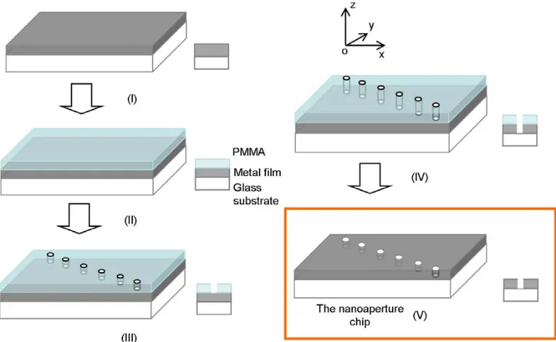
3.1 Fabrication of the nanoaperture array... 43
3.2 Fabrication of microfluidic chips... 46
3.3 Assembly of the nanoaperture chip with the microfluidic chip ... 49
Chapter 4: Applications in Nematode Imaging and Phenotype Characterization ... 53
4.1 Characterization of the imaging properties of the OFM prototype... 53
4.2 Imaging of C. elegans larvae ... 59
4.3 Characterization of two genotypes of C. elegans... 61
5.2 Simulation scheme: Finite Element Methods (FEM) ... 75
5.3 Simulation implementation : COMSOL Multiphysics ... 81
Chapter 6: Experimental investigation of collection-mode OFM: type II ABID... 95
6.1 Experimental scheme: ‘walking-tip’ methods ... 95
6.2 Summary of both the experimental results and the simulation results ... 101
6.3 The ‘finite-NA’ problem and our treatment ... 107
6.4 Comparison of nanoaperture based imaging systems with conventional microscopes ... 112
Chapter 7: Integration of Optical Tweezers with grid-based OFM ... 116
7.1 Motivation ... 116
7.2 Optical tweezers and the instrumentation... 118
7.3 Grid based OFM: operating principles and fabrication... 127
7.4 Application in high resolution OFM... 136
Chapter 8: Conclusion of my thesis ... 143
8.1 Summary of my graduate work... 143
8.2 Preliminary results of new OFM functions ... 149
LIST OF FIGURES
Chapter 1:
Fig. 1-1: Pressure driven flow in circular channel……….4
Fig. 1-2: Illustration of electroosmosis…..………6
Fig. 1-3: Examples of optofluidic sensing or imaging devices………...…….12
Fig. 1-4: Examples of nanoaperture assisted devices………..………16
Chapter 2:
Fig. 2-1: Illustration of an infinity-optics system………..…...21Fig. 2-2: Illustration of near field scanning microscopy (NSOM)………...…24
Fig. 2-3: Two feedback control mechanisms for NSOM ..……….…...26
Fig. 2-4: Total internal reflection fluorescence microscopy………...….27
Fig. 2-5: A compact OFM compared with a US quarter……….…....28
Fig. 2-6: The flow diagram of OFM design………..…..30
Fig. 2-7: Two designs of OFM………..….32
Fig. 2-8: Illustration the image formation process of OFM………..…..33
Fig. 2-9: Top view of the first OFM prototype & examples of transmission time traces from two apertures………34
Fig. 2-10: Illumination mode OFM & nanoaperture grid based OFM………...36
Fig. 2-11: Illustration of SPP assisted OFM………..38
Fig. 2-12: Schematic of an OFM design based on nanoaperture ‘bundle’………...39
Fig. 2-13: Fluorescence OFM………40
Chapter 3:
Fig. 3-1: Fabrication procedure of the nanoaperture array………44Fig. 3-3: Fabrication of the fluidic chip………...… 48
Fig. 3-4: Camera images of the nanoaperture array with an isolated aperture…………..50
Fig. 3-5: Infrastructure of an OFM device: a hybrid approach……….51
Chapter 4:
Fig. 4-1: Schematic of the first OFM prototype……….….. 54Fig. 4-2: Photograph of the experimental setup………....55
Fig. 4-3: Illustration of the experimental setup……….56
Fig. 4-4: The time-of-flight signal from Aperture No. 60 of the array………..58
Fig. 4-5: OFM images of C. elegans larvae………..59
Fig. 4-6: Aspect ratio map of wild type and dpy-24 C. elegans………61
Fig. 4-7: Experimental scheme of measure the resolution limit of the device………..…63
Fig. 4-8: Characterization of the achieved resolution from the images………64
Chapter 5:
Fig. 5-1: Diagram and photos of the near field microscope system (alpha-SNOM, WITec Gmbh……….………….69Fig. 5-2: Two schemes of aperture based imaging devices………...70
Fig. 5-3: Resolution of type I ABID………..71
Fig. 5-4: A representative FDTD cubical………..74
Fig. 5-5: Transmission SNR curves for varying aperture sizes..………...78
Fig. 5-6: Mesh grid for FEM and FDTD………...79
Fig. 5-7: Schematic of the simulation geometry of type II ABID………..82
Fig. 5-8: Example of one simulation result………84
Fig. 5-9: Simulation generated CPSF plots for three different sample-nanoaperture separation………85
Fig. 5-10: FWHM of CPSF v.s. gap size (H) for a range of aperture sizes…………....…87
Fig. 5-11: Schematic of the computation of the nanoaperture transmission………...89
Chapter 6:
Fig. 6-1: Schematic of type II ABID….……….………...96
Fig. 6-2: Illustration of experimental schemes………..………98
Fig. 6-3: NSOM measurement of a nanoaperture at different H………..100
Fig. 6-4: FWHM of CPSF v.s. gap size (H) for a range of aperture sizes (realistic NSOM tip scenario)………...…..101
Fig. 6-5: FWHM of CPSF v.s. gap size (H) for a range of aperture sizes (pseudo point source scenario)……….………...…...102
Fig. 6-6: 2D cross sectional plot of the transmitted wave from a 550nm aperture……...104
Fig. 6-7: Investigation of the ‘limited NA’ issue of a 300nm aperture……….108
Fig. 6-8: Investigation of the ‘limited NA’ issue of a 550nm aperture……….110
Fig. 6-9: Comparison of type II ABIDs with conventional microscopy………...113
Chapter 7:
Fig. 7-1: Setup of the optical tweezer system……….………..119Fig. 7-2: Calculation of the strength of the optical tweezer………..121
Fig. 7-3: Calculation of the strength of the optical tweezer (cont’d)………....123
Fig. 7-4: Experimental measurement of the strength of the optical tweezer……….124
Fig. 7-5: Improvement of the sample jittering by adding a fluidic chamber……..……...126
Fig. 7-6: Images of the nanoaperture grid device………..…...127
Fig. 7-7: Illustration the propagation and damping of the SPP waves………...…...129
Fig. 7-8: Measurement of the resolution limit………..…....130
Fig. 7-9: Illustration of the imaging part………..……133
Fig. 7-10: Example of a microsphere passing the nanoapertures………..…...133
Fig. 7-11: Orientation of the nanoaperture grid and the direction of the sample transportation………...………134
Fig. 7-12: Illustration of the entire experimental setup………..………..136
Chapter 8:
Fig. 8-1: OFM design………..……….………144
Fig. 8-2: OFM images of C. elegans and the morphology map………...…….145
Fig. 8-3: Two schemes of ABIDs……….146
Fig. 8-4: Resolution of type II devices……….146
Fig. 8-5: Arrangement of the nanoaperture grid, fluidic chamber and the objective lens & nanoaperture array v.s. nanoaperture grid………...147
Fig. 8-6: OFM images of a few representative samples………...148
Fig. 8-7: Setup of the entire imaging system (nanoaperture grid + optical tweezer)....150
Fig. 8-8: Experimental procedure of fluorescence imaging and a few images……….151
Fig. 8-9: Illustration of EK enabled OFM………153
LIST OF TABLES
Chapter 5:
Table 1: Depth of field of a few subwavelength apertures…...………..……….……....82
Chapter 6:
Table 1: Summary of the investigation of the limited NA issue of two
different aperture sizes….………..……….……….105
Chapter 7:
LIST OF FREQUENTLY USED ACRONYMS
Acronym Full name
ABID Aperture Based Imaging Device FEM Finite Element Methods
CPSF Collection-mode Point Spread Function
NSOM Near-field Scanning Optical Microscope/Microscopy OFM Optofluidic Microscope/Microscopy
C h a p t e r 1
OVERVIEW
Microfluidics is a multidisciplinary area that brings together the experts from both engineering and fundamental sciences. Optofluidics, as a specialized field of microfluidics, has not drawn much attention until very recently, when optical engineers started to recognize the unique properties of microfluidics and their huge potentials in creating novel optical devices. In this chapter, I will introduce the basics of microfluidics with special attention to microfluidic detection techniques. The physics and technology involved is closely related to the focus of my thesis: Optofluidic Microscopy. In addition, recent research on nanoapertures and their applications in optoelectronics and biology will be introduced.
1.1 Basic microfluidics
Microfluidics, as the name suggests, studies the behavior of fluid in a tiny volume from micro-liters down to pico-liters. Subsequently, the discoveries made in investigating fluidic flow in microfluidics can be used in a large number of applications, such as for controling fluid and manipulating biological samples. The length scale of microfluidics normally ranges from 10 μm to 100 μm, while there has been increased interest in studying fluid flow in sub-micrometer channels.
In fluidic mechanics, the Reynolds number (Re), as arguably the most important dimensionless number, equals to the ratio of inertial forces and viscous forces. It is expressed as follows:
(1.1) /
/
Re 2
2
P U P
U vL
L v
L v
where is the density of the fluid or the target object, v is mean fluid velocity, L is the characteristic length, and is the dynamic viscosity of the fluid. Laminar flow, which occurs at low Re, is characterized by smooth, constant fluid motion. Turbulent flow, on the other hand, occurs at high Reynolds numbers and produces random vortices and other flow fluctuations.
In pipe flows, Re <= 1500 usually indicates laminar flow. Let us take the biofluidic platform as an example to estimate the Reynolds number. The medium of biofluidics is usually water with =1.0 x 10³Kg m-3 and μ=1.002 x 10⁻³ N s/m2 (at 20oC). The velocity of the fluid flow does not normally surpass 10 mm sec-1; the hydraulic diameter (L) [1] of the microchannel is usually not larger than 1.0 mm. By applying the abovementioned parameters into Eq. (1.1), the Reynolds number of this exemplary pipeline flow is Re ~ 10, indicating a laminar flow situation. In my experiments, both the flow velocity and the characteristic length scale are one or two orders smaller than the numbers given here. Hence, I would only need to focus on the behaviors of low Re flow.
The fact that microfluidics is usually described by low Reynolds numbers has significant implications. The well-predictable behavior of micro channel flow makes it easy to apply microfluidic technology to manipulate fluid and transport biological samples. That is to say, a great amount of time and labor can be saved from investigating the complexity of the fluid motion. This particular property of the micro flow is a fundamental driving force behind the proliferation of microfluidic research in various areas of biology and optics. Besides that, microfluidic devices certainly have a few other important advantages such as compactness, low cost and low sample consumption.
community. I will only use the most simplistic models to describe the fundamental properties of each actuation scheme. Throughout our discussion, I will assume that the fluid we are studying is incompressible and Newtonian (Newtonian: the stress is proportional to the strain rate).
(1) Pressure driven flow
The behavior of a fluid, which is incompressible, Newtonian, isotropic, and obeys Fick’s law of thermal conductivity, is governed by the Navier-Stokes equation, which actually represents the continuum version of F=ma on the basis of per-unit-volume [1, 2]
(1.3) 0 (1.2) ) ( 2 w w v v v t v v p
f P U U
which represents the conservation of momentum and mass, respectively. p is the pressure, f
is the body force. The boundary conditions for such a fluid are usually no-slip, no temperature jump at the boundaries.
However, for low Reynolds number flow, the inertial effects, i.e. the right hand side of Eq. (1.2), are so small that they can be neglected. Then, the Navier-Stokes equation is further simplified: (1.4) 0 2 v p
f
Parallel flow (Fig. 1-1(a)) in long, straight micro channels is one of the most fundamental phenomena in microfluidics. Besides its simplicity, it has direct relevance to Optofluidic Microscopy, where stable sample delivery in straight channels is desirable. Therefore, I would like to use parallel flow to describe some of the most significant properties of pressure drive flow.
(1.6) 8 (1.5) 4 2 2 2 ) dz dp ( R dA v Q ) -r (R -dp/dz vz
³
xwhere R is the radius of the circular channel; is the flow rate. Sample that travels in the micro channel tend to have the same velocity as the fluid in order to minimize the Stokes’s drag (e.g. Eq. (1.7) for small spherical objects [1]) between the sample and the fluid. However, such an “equi-velocity” trend assumes that there is no other frictional force existing in the force diagram. In the case of C. elegans traveling in micro channel, such an “equi-velocity” condition may not hold. In this particular example, the nematode may also feel the drag force from the channel walls, which makes the worm travel slower than the fluid itself.
x Q
F 6Rv (1.7)
Note that Eq. (1.7) only applied to a rigid and spherical object in Stokes flow. Modification to such a formula is required for real objects.
y x
z, vz
r
R
boundary boundary
vz, max
vz=0
(a) (b)
Figure 1-1: Pressure-driven flow in circular channel. (a) Geometry of the parallel flow. R: radius of the channel. (b) The velocity profile is parabolic for such an example of parallel flow.
proportional to and thus, one can tune the velocity by controlling the pressure drop between the inlet and outlet of the micro channel. This type of fine-tuning can be readily accomplished by using a syringe pump, which usually has an accurate setting of flow rate. One such syringe pump is made by Harvard Instruments: Harvard Apparatus PicoPlus 11. Second, the flow profile is parabolic (Fig. 1-1(b)), indicating that the flow speed (v) is at maximum at the center of the channel, while v reduces to zero at the boundary. Therefore, a sample, such as a mammalian cell that is not flowing in the center of the channel, would see a velocity difference at its top and its bottom, as shown in Fig. 1-1(b). This velocity difference would give a torque to the sample, possibly causing it to rotate quickly. Thirdly, the central velocity is proportional to R2. This second-order scaling law (Eq. (1.5)) points out that the highest fluid velocity that can be experimentally achieved drops very fast with the channel size. That is to say, the smaller (or narrower) the channel were, the lower the achievable velocity would be, when assuming the pressure gradient remains as a constant. It implies that high flow rate, i.e. high-throughput sample delivery, will be extremely difficult to accomplish in the regime of nanofluidics- the dimension of the channel is not larger than 100 nm. As such, fluidic actuation in the nanofluidic regime is often accomplished by electrokinetic pumping, which is independent of the size of the channel, as will be shown in Eq. (1.11).
dp/dz
(2) Electrokinetic pumping
We can roughly divide electrokinetics into two categories: electroosmosis, which refers to the motion of polar liquid, e.g. water, under the influence of electric field, and electrophoresis, which refers to the motion of a charged material, e.g. a biological cell, under the electric field.
of the ions in the liquid, and a mean field approximation for the ions within the electric field, the electrical potential () can be derived [2],
(1.10) 2 (1.9) (1.8) exp 2 1 2 0 0 / B w D w D D e n T k q y ¸¸¹ · ¨¨© § ¸¸¹ · ¨¨© § O M
where is called the zeta-potential of the wall, which is determined by surface charge density (q0), dielectric constant of the wall (w), and Debye length (D). Debye length in Eq. (1.10) depicts the effective thickness of the EDL. It can be seen from Eq. (1.8) that outside EDL, the electrical potential is close to a constant. Note that in order to obtain the above equations, it has been assumed that the thickness of EDL (i.e. the Debye length) is much smaller than the length scale of the channel. Fortunately, this assumption is usually valid as the Debye length is no larger than 10nm for most microfluidic systems, including Optofluidic Microscope (OFM).
Potential w 0 D Stern layer Diffuse layer y x [
+ P
-EDL
HE
(a) (b)
v
EDL
This electrical potential can be added to the Navier-Stokes equation (Eq. 1.4) as an external force (E·E) to calculate the electroosmotic flow (EOF), when E is the electrical field applied along the direction of the long channel. After applying the appropriate boundary conditions, the velocity of EOF outside the EDL can be written as:
(1.11) P [HE
vEOF
which is linear to the applied electrical field, E (Fig. 1-2(b)) and is independent of the channel size.
The flat velocity profile of EOF can immediately benefit the OFM - the samples transported by electrokinetic pumping, in principle, would not rotate in the channel because the flow velocity is a constant outside the EDL. Note that pressure gradient and electroosmosis may both exist in an electrokinetic pumping experiment. Because of the linearity of the simplified Navier-Stokes equation (Eq. 1.4), the electroosmotic velocity derived here can directly be added to that obtained with pressure driven flow (Eq. 1.5) to find the collective results of the two forces.
On the other hand, electrophoresis studies the manipulation of samples through the use of the electrical field. The movement of a small spherical object in a low Reynolds number environment can be described as the balance between the viscous Stokes drag (Eq. 1.7) and the Coulomb force (qs·E) (Ref. [1]),
(1.12) 6Rv E
qs
Note that qsis the screened surface charge of the spherical sample, which can be calculated by using the same method that derives Eq. (1.8).
The size of the charged sample inside the fluid can be very different. It could be much larger than D, such as a micron-sized latex sphere; or the size of the object can be much smaller than D, such as nanoparticles. However, in both limits, the resulting electrophoretic (EP) velocity of the sample is proportional to
P [HE
zeta potential ( ) here is the property of the sample surface, rather than that of the microfluidic wall as in Eq. (1.11).
Sample manipulation by using electrokinetic pumping is popular among the microfluidic community as electrokinetics utilizes surface forces, which scale well with channel’s length scale. When the size of the channel gets to the level of 100 nanometers, electrokinetic pumping will be more effective than pressure gradient pumping. In addition, the components of the electrokinetic pump, such as the microelectrode arrays, are easy to integrate into a microfluidic system, so that the entire microfluidic system can be made compact and energy-efficient.
In the end, I want to point out that when drawing the simple conclusions in (1) pressure driven flow and (2) electrokinetic pumping, I have assumed that the object immersed in the liquid medium is far away from the channel wall and the object is perfectly rigid without any deformation caused by the fluid field. The situation would get much more complicated when the size of the object is comparable with the fluidic channel and/or the object is very close to the channel wall. Curious readers can read Ref. [2-4] and their cited literature in order to get more insight about flow or diffusion behavior of the object in the near-wall situation.
(3) Dielectrophoeresis and other actuation schemes
Dielectrophoresis (DEP) deals with the motion of polarizable particles, like cells, subject to a non-uniform AC electrical field. It has becomes quite popular lately because of its capability of trapping nanometric particles within very confined geometry, e.g. smaller than 1 micron. A polarized particle can be approximated as a summation of electric dipoles, whilst the description of the dielectrophoresis of dipoles can be accurate. When using an electrostatic approximation, the time-averaged DEP force can be expressed as follows [1, 5],
(1.14) 2 ) ( (1.13) ) ( Re2 3 2
where a is the radius of the particle; Erms2 is the gradient of the square of the rms electrical field. The Clausius-Mossotti factor, K(), is determined by the complex permittivity of the particle (p) and the medium (m). The sign of the real part of K()
determines whether the DEP force is toward the higher field intensity or away from it. For DEP trapping, Re
K(Z) needs to be larger than zero; in such a case, the particles move toward the fabricated electrodes, near which the electrical field is highly concentrated, i.e. higher Erms 2 . Although DEP force has a short working range, it has also been demonstrated in transporting particles in a long distance. In DEP transportation experiments, inter-digitated microelectrode array is fabricated underneath the fluidic channel; the samples start to move when the individual microelectrode turns on and off inter-digitally. This phenomenon is somewhat similar to peristaltic pumping.Recently, optical tweezers have drawn lots of attention within the microfluidics community due to their superior ability to position and control objects beyond the capability of other sample actuation means. Under the dipole approximation, the gradient force applied on the object is similar in expression as the DEP situation, in the sense that any object with a larger refractive index than that of the medium prefers to move toward higher intensity, i.e. larger . More details of employing optical tweezer actuation in microfluidics will be given in Chapter 7, which reports on our development of the first optical-tweezer actuated OFM.
laser
I
Electrowetting is probably one of the simplest means of driving microfluidic motion [2]; it works by modifying the surface tension between the solid phase and the liquid phase, i.e.
2
2
CV o sl o
sl oJ
J , where Jsl refers to the surface tension at solid-liquid interface;
t
C HrHorefers to the capacitance at the interface for a uniform dielectric of thickness t; and
V is the applied voltage.
As such, the modified Young-Dupre equation, or say Lippmann’s equation [2] is
(1.15) 2
cos
2
sg o
sl gl
CV J J
T
where is the contact angle.
When a potential difference is applied between the droplet and the substrate, the droplet starts to spread on the surface and lower the contact angle. It is said that droplet manipulation by using electrowetting can be as fast as 1 mm/s [2]. As such, samples or reaction agents encapsulated in an electrolytic droplet can possibly move at high speed on the surface of the substrate. However, electrowetting may suffer from electrolysis or excessive Joule heating.
Besides the abovementioned methods, another few microfluidic actuation schemes will probably benefit optofluidic applications. These schemes include but are not limited to optoelectronic tweezers [6], photo-thermal fluidic pumping [7], magnetic tweezers [8], and thermo-capillary actuation [9].
1.2 Microfluidic detection, sensing and imaging using optical means
Microfluidic detection is of significant use. For example, microfluidic mixing needs to be visualized in an easy-to-understand format, so that fluid physicists can investigate the pattern and the dynamics of the mixing process. As such, an appropriate detection method has to be employed which does not interrupt with the natural dynamic evolution of the fluidic mixing. In addition, data obtained from microfluidic detection is important in analyzing chemical reactions, development of biological cells, etc.
Microfluidic detection can be achieved in various ways that can make use of impedance change, temperature change, change in optical signals, etc. In this section, I will only focus on optical detection methods that have been massively employed in microfluidic systems.
There are many aspects of light that can be targeted as a detection subject. Accessible optical information includes intensity of light as in bright field microscopes, phase change of light as in optical interferometers, and the angular spectrum of the scattered light. Furthermore, nonlinear optical signals, such as fluorescence, second harmonic waves, and Raman scattering signals add another dimension to the field of optical detection. One major advantage of using nonlinear optics is that the acquired data have excellent contrast and are easy to visualize because light at the fundamental wavelength (0) can be very efficiently
An exhaustive summarization of all the optofluidic detection methods is impractical considering the length of my thesis. As a result, I will concentrate on only a few examples of lab-on-chip detection schemes. Alongside, some of the fundamental properties of optofluidic detection will be discussed.
The first example is particle image velocimetry (PIV). PIV, as the name suggests, measures the velocity of the particles seeded in the fluid by using the time-lapse images of the particles. A PIV system takes two images shortly after each other and then calculates the distance individual particles traveled within this time. By knowing the time difference and the measured displacement, the velocity is calculated in the end. This technique can have both a high temporal resolution (~10 ns) and a high spatial resolution (~1 μm). The equipment required by a basic PIV system is similar to an optical microscope, except that a “light-sheet” illumination is needed in PIV [10]. As there are still many poorly understood aspects of microfluidics, such as micro-mixing, the PIV techniques will certainly benefit the development of novel microfluidic systems.
(a)
(b)
[image:27.612.128.519.130.388.2](c) (d)
Figure 1-3: Examples of optofluidic sensing or imaging devices. (a) Micro-FACS. The appearance of fluorescence signals at the ‘detection window’ triggers the opening of the collection reservoir. Reprint permission from Ref. [11]. (b) Microfabricated Young’s interferometer sensor was used in virus detection. 1, 2, and 3 indicate the measuring channels, and 4 is the reference channel. Reprint permission from Ref. [14]. (c) Microfabricated confocal microscopy by using MEMS technology. Two micro-lens scanners are orthogonally aligned and vertically stacked. Reprint permission from Ref. [15]. (d) Electrowetting enabled tunable lenses for cell phone cameras. Schematic shows the cross section of a liquid-based variable lens in a cylindrical glass housing. The transparent electrodes are formed of 50-nm-indium tin oxide; the insulator is a 3-mm-parylene-N layer. Reprint permission from Ref. [16].
biosensing. That is to say, the attachment of molecules, such as proteins, onto one arm of the sensor surface will cause a miniscule change in the refractive index of the arm, which is expressed as a tiny drift of the light phase. Optical interferometry can measure the phase drift, and subsequently the change in refractive index (n) down to a high level (e.g., n ~ 10-6 in [12], n ~ 10-8 [13]). Recently, Ymeti et al. [14] reported on an integrated Young’s interferometer sensor that was applied to detect HSV-1 virus (Fig. 1-3(b)). This integrated device represents a broad range of micro interferometers that can make biosensing much cheaper and more compact compared with a lab-bench system.
The microscope objective lens is arguably the most critical component of an optical microscope. As such, investigation into microfabricated lenses will certainly enable miniaturized optical microscopes. In fact, a range of compact lenses have also been designed by groups around the world. For example, Luke P. Lee’s group [15] developed a micromachined confocal microscope that was enabled by electrostatic actuation of two polymer micro lenses (Fig. 1-3(c)). This technology will potentially make possible the integration of a confocal microscope array onto a single chip. However, very sophisticated fabrication technology will be required in order to design a miniaturized objective lens and match the imaging quality of a regular microscope objective. In 2004, Philips Research announced one of the first microfluidic optical lenses (Fig. 1-3(d)) [16]. The device made use of the electrowetting effect, that is, the shape of an oil-water interface was modulated through electrical manipulation of the contact angle. This liquid lens is particularly useful in electronic devices such as cell phone cameras, where the demand on image quality is not so stringent.
1.3 Nanoapertures and their applications
and/or, in many cases, the existence of surface plamson waves makes the effective optical size of the nanoaperture much larger than its physical size.
Bethe was probably the first to study nanoapertures in optics. In his original paper in 1944 [17], he theoretically calculated the transmission through the nanoaperture that was drilled in an infinitely thin but perfect conductor. Bethe’s model predicted that the transmission power after being normalized by the aperture’s area scaled as DO 4, where D
is the aperture diameter, and is the wavelength. Later on, Bouwkamp [18] improved Bethe’s result by deriving additional terms for the expansion, whose first three terms may be written as [18, 19],
(1.16) 2 375 18 7312 2 25 22 2 27 64 10 8 8 6 6 4 2 kD , kD kD D T » ¼ º « ¬ ª
Where T is the transmission coefficient [17, 18]; and k is the wave vector. Note that the derivation of such a relation was based upon a square aperture with dimensions D x D
illuminated by a plane wave at normal incidence. The results for a circular aperture can also be found in Bouwkamp’s classical paper [18].
Nanoapertures are known to possess interesting optical properties. Near-field light components, normally too weak or say “too evanescent” to be detectable, are scattered by the nanoapertures and become discernible with a far field detector. For example, a nanoaperture based near field microscope can render a high resolution far beyond the diffraction limit [20].
More recently, there is a seminal work done by Ebbesen et al. [21], which for the first time connected surface plasmon waves with the 2D nanoaperture array. It was discovered that transmission through a tightly-spaced nanoaperture array could be dramatically enhanced compared to the summation of that of all the individual and isolated nanoapertures.
photolithography. Therefore, I will devote this section of my thesis to the overview of the applications of nanoapertures that are closely relevant to lab-on-a-chip and optofluidics.
The first example focuses on specially engineered non-circular nanoapertures. Although circular nanoapertures can render a superior high resolution when used in imaging or sensing, they also suffer from exceedingly weak transmission. For example, transmission through a 30nm aperture is three orders-of-magnitude weaker than that through a 100nm aperture.
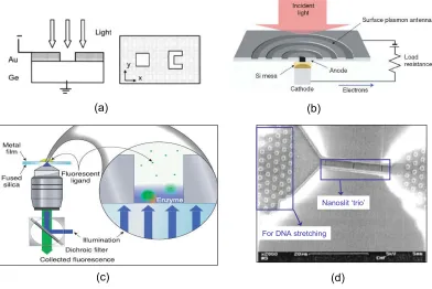
Such a weak signal issue requires that, in practice, either the acquisition time needs to be elongated or an ultra sensitive detector is necessary. Consequently, the increased consumption in time and cash really limit the ultimate usefulness of the nanoapertures. Therefore, a few labs have been working on innovative nanoaperture designs in order to enhance the transmission without necessarily enlarging the region, within which the light is confined. Hesselink’s group in Stanford and Xu’s group in Purdue are two of the pioneers in designing C-shaped [22, 23] or H-shaped [23] nanoapertures with enhanced optical transmission. The three-orders-of-magnitude improvement in transmission and 0.1 confined spot size [22] were contributed by both the propagation modes from these so called “optical ridge-waveguides” structure and local surface plasmons around the aperture. On the application side, such “optical ridge-waveguides” have proved to be useful in improving the performance of photo-detectors (Fig. 1-4 (a)) [24], very small aperture lasers [25], and lithography technology.
For DNA stretching
Nanoslit ‘trio’
(a) (b)
[image:31.612.126.518.131.393.2](c) (d)
Figure 1-4: Examples of nanoaperture assisted devices. (a) Germanium photodetector improved by “optical ridge-waveguide”, i.e. the “C” aperture. The apertures are formed in a Au film on top of a Ge substrate. The device is reverse-biased, and it functionsas a Schottky diode. Reprint permission from Ref. [24]. (b) Nano photodiode with a surface plasmon antenna. Reprint permission from Ref. [28]. (c) Zero-mode waveguide for spectroscopy applications. Reprint permission from Ref. [29]. (d) Nanofluidic near field scanner for DNA measurement. SEM image shows three 100 nm wide slits and hydrodynamic channels nanofabricated into an etched quartz structure. Reprint permission from Ref. [30].
transmission. It was indicated that the interplay between light and surface plasmon would not have occurred unless the condition of conservation of momentum was satisfied, i.e.
(1.17)
// G
K
Ksp r
where Ksp is the momentum of surface plasmon waves; K// is the component of the incident wave-vector in the plane of the nanoaperture array; and G represents a series of the reciprocal wave-vectors provided by the periodic surface corrugation or the nanoaperture array lattice. There is an excellent review article in Nature [27] that summarizes the potential applications of the nanoaperture array in numerous areas, such as optoelectronics (Fig. 1-4(b), also from Ref. [28]).
Moreover, in many occasions, even a single and isolated aperture could be of significant use. As the tiny nanoaperture does not support any waveguide modes, optical waves are largely confined within a femtoliter volume. It has been reported that the fluorescence intensity inside confined geometry is markedly enhanced due to an increase of the excitation wave and the reduction of the fluorescence lifetime within a nanoaperture. Michael Levene and his colleagues [29] successfully applied such an isolated nanoaperture in fluorescence correlation spectroscopy (Fig. 1-4(c)), which is a powerful technique to study the diffusion and reaction rate of single biomolecules. One major advantage of such a “zero-mode waveguide” is that it allows for the study of biophysical events of the molecules at their normal physiological conditions, i.e. millimolar concentration. Nevertheless, most of the then-existing single molecule studies required the dilution of the biomolecules solution down to pico- or nano-moles.
preliminary work on measuring the length of uncoiled DNA molecules (Fig. 1-4(d)). Their achieved resolution of 200 nm was a clear indication that nanoslits are able to render a high resolution beyond the diffraction limit.
Concluding remarks of this chapter
Both microfluidics and nanoapertures have drawn tremendous interest within the research community. The enormous advantages brought with microfluidics can perfectly combine with the unique properties of nanoapertures thanks to the planar nature of the fabrication technology involved. There have been preliminary research results showing the vast potentials of microfluidic based nanoaperture devices in numerous applications areas in biology, and I have briefly listed a few of them. OptoFluidic Microscopy, which will be discussed in details for the rest of my thesis, is certainly an excellent example of the perfect fusion of microfluidics and nanoapertures.
References
1.N. T. Nguyen, and S. T. Wereley, Fundamentals and Applications of Microfluidics (Artech House, 2002).
2.T. M. Squires, and S. R. Quake, "Microfluidics: Fluid physics at the nanoliter scale," Reviews of Modern Physics 77, 977-1026 (2005).
3.R. F. Ismagilov, A. D. Stroock, P. J. A. Kenis, G. Whitesides, and H. A. Stone, "Experimental and theoretical scaling laws for transverse diffusive broadening in two-phase laminar flows in microchannels," Applied Physics Letters 76, 2376-2378 (2000).
4.A. E. Kamholz, and P. Yager, "Molecular diffusive scaling laws in pressure-driven microfluidic channels: deviation from one-dimensional Einstein approximations," Sensors and Actuators B-Chemical 82, 117-121 (2002).
5.W. M. Arnold, "Positioning, levitation and separation of biological cells," in Electrostatics 1999(1999), pp. 63-68.
6.P. Y. Chiou, A. T. Ohta, and M. C. Wu, "Massively parallel manipulation of single cells and microparticles using optical images," Nature 436, 370-372 (2005).
7.G. L. Liu, J. Kim, Y. Lu, and L. P. Lee, "Optofluidic control using photothermal nanoparticles," Nat Mater 5, 27-32 (2006).
8.H. Lee, A. M. Purdon, and R. M. Westervelt, "Manipulation of biological cells using a microelectromagnet matrix," Applied Physics Letters 85, 1063-1065 (2004).
10.R. J. Adrian, "Twenty years of particle image velocimetry," Experiments in Fluids 39, 159-169 (2005).
11.A. Y. Fu, C. Spence, A. Scherer, F. H. Arnold, and S. R. Quake, "A microfabricated fluorescence-activated cell sorter," Nature Biotechnology 17, 1109-1111 (1999).
12.T. Allsop, R. Reeves, D. J. Webb, I. Bennion, and R. Neal, "A high sensitivity refractometer based upon a long period grating Mach-Zehnder interferometer," Review of Scientific Instruments 73, 1702-1705 (2002).
13.J. Zhang, Z. H. Lu, B. Menegozzi, and L. J. Wang, "Application of frequency combs in the measurement of the refractive index of air," Review of Scientific Instruments 77 (2006). 14.A. Ymeti, J. Greve, P. V. Lambeck, T. Wink, S. van Hovell, T. A. M. Beumer, R. R. Wijn, R. G. Heideman, V. Subramaniam, and J. S. Kanger, "Fast, ultrasensitive virus detection using a young interferometer sensor," Nano Letters 7, 394-397 (2007).
15.S. Kwon, and L. P. Lee, "Micromachined transmissive scanning confocal microscope," Optics Letters 29, 706-708 (2004).
16.S. Kuiper, and B. H. W. Hendriks, "Variable-focus liquid lens for miniature cameras," Applied Physics Letters 85, 1128-1130 (2004).
17.H. A. Bethe, "Theory of diffraction by small holes," Physical Review 66, 163-182 (1944). 18.C. J. Bouwkamp, "Diffraction theory," Reports on Progress in Physics XVIII, 35 (1954). 19.T. Vallius, and J. Turunen, "Transmission through single subwavelength apertures in thin metal films and effects of surface plasmons," Journal of the Optical Society of America a-Optics Image Science and Vision 21, 456-463 (2004).
20.D. Courjon, Near-field microscopy and near-field optics (London: Imperial College Press, 2003). 21.T. W. Ebbesen, H. J. Lezec, H. F. Ghaemi, T. Thio, and P. A. Wolff, "Extraordinary optical transmission through sub-wavelength hole arrays," Nature 391, 667-669 (1998).
22.X. L. Shi, L. Hesselink, and R. L. Thornton, "Ultrahigh light transmission through a C-shaped nanoaperture," Optics Letters 28, 1320-1322 (2003).
23.E. X. Jin, and X. F. Xu, "Obtaining super resolution light spot using surface plasmon assisted sharp ridge nanoaperture," Applied Physics Letters 86 (2005).
24.L. Tang, D. A. B. Miller, A. K. Okyay, J. A. Matteo, Y. Yuen, K. C. Saraswat, and L. Hesselink, "C-shaped nanoaperture-enhanced germanium photodetector," Optics Letters 31, 1519-1521 (2006).
25.F. Chen, A. Itagi, J. A. Bain, D. D. Stancil, T. E. Schlesinger, L. Stebounova, G. C. Walker, and B. B. Akhremitchev, "Imaging of optical field confinement in ridge waveguides fabricated on very-small-aperture laser," Applied Physics Letters 83, 3245-3247 (2003).
26.H. J. Lezec, A. Degiron, E. Devaux, R. A. Linke, L. Martin-Moreno, F. J. Garcia-Vidal, and T. W. Ebbesen, "Beaming light from a subwavelength aperture," Science 297, 820-822 (2002). 27.C. Genet, and T. W. Ebbesen, "Light in tiny holes," Nature 445, 39-46 (2007).
28.T. Ishi, J. Fujikata, K. Makita, T. Baba, and K. Ohashi, "Si nano-photodiode with a surface plasmon antenna," Japanese Journal of Applied Physics Part 2-Letters & Express Letters 44, L364-L366 (2005).
29.M. J. Levene, J. Korlach, S. W. Turner, M. Foquet, H. G. Craighead, and W. W. Webb, "Zero-mode waveguides for single-molecule analysis at high concentrations," Science 299, 682-686 (2003).
C h a p t e r 2
THEORY OF OPTOFLUIDIC MICROSCOPY
Optofluidic Microscopy (OFM) combines advanced microfluidic technologies and the nanoaperture-based imaging technique to produce a “microscope-on-a-chip”. Unlike conventional microscopes, OFM does not require the use of an objective lens. Nor does OFM need sophisticated machinery for sample actuation and feedback control, which is always necessary for a commercial near-field optical microscope. In this chapter, I will first introduce the fundamental concepts of conventional microscopy and near field microscopy. After that, I will explain in details the working principles of OFM. In the discussion, the relationship and difference of the abovementioned imaging techniques will be highlighted. At the end, I will introduce a few designs of OFM that either have already been implemented or should be implementable in near future.
2.1 Overview of conventional microscopy and near field imaging
1) Basic concepts of conventional microscopy
Microscopic objects are usually too small to be seen with naked eye. Conventional microscopes are optical instruments that can produce magnified images, real or virtual, of objects. Therefore, the conventional microscope must accomplish two tasks: produce a magnified image of the specimen, and render the details in a way that human eyes or a photo detector (e.g., camera) can read or record.
the objective lens, as the most important microscope component, still plays the major role in image formation and determining the image quality. Therefore, it is quite straightforward to lay out a few important properties of a conventional microscope. Here I would like to discuss them within the frame of infinity-optics system.
Such a microscope system (Fig. 2-1) usually includes an illumination source, such as a lamp or a laser, a microscope objective, a tube lens, and a sensitive camera (or other recording media). During image formation, the object of interest is placed on the focal plane of the objective lens. In an infinity-corrected optical system, the exit light rays after the objective lens are made up of plane waves with a focal point in the infinity. In this case, a tube lens (or say a camera lens) is necessary to re-focus the light and form an image. On the image plane, we normally place a high-quality camera (Fig. 2-1) and then read the images on a computer screen.
Objective illumination
Object
‘Infinity space’
Tube lens (camera lens)
Image
Camera
Figure 2-1: Illustration of an infinity-optics system. The object is located on the focal plane. The output from the objective lens is made up of plane waves. “Infinity space” is the space between the objective lens and the tube lens, between which various optical components can be inserted.
magnification, M= 200mm/4.5mm ~ 44. Usually a 100X objective lens can magnify the object by 100 folds, and thus enables the study of the real sub-micron details of the object.
One major advantage of an infinity-corrected system over its finite-optics counterpart is that numerous auxiliary components, such as waveplates, pinholes, and polarizers, can be inserted into “the infinity space” (see Fig. 2-1) without having to worry about the possibility of any spatial shift or directional change of the light ray. Thereafter, over the past two decades, all the major microscope manufacturers have gradually migrated to the deployment of infinity optical systems when producing research-grade microscopes.
The resolution of a conventional microscope impinges on the so-called diffraction limit, which arises from the size of the spot that a light beam can be focused to with normal lens elements. At the focal point, the beam forms a symmetric pattern of concentric rings known as the Airy disk pattern, which was first described in detail by Ernst Abbe in 1873. The Airy disk can be fully formulated using the scalar diffraction theory [1].
The distance, R, from the highest intensity point located in the middle of the center spot to the first node in intensity is given by
(2.1) 61
. 0
NA
R O
where is the wavelength; NA is the numerical aperture of the objective lens. Mathematically, under Rayleigh’s criterion [2], R denotes the resolution limit of such a lens-based imaging system.
biological cells. That is the primary reason behind the invention of a variety of contrast enhancement mechanisms, such as differential interference contrast (DIC)
2) Basic concepts of near field scanning optical microscope (NSOM)
The concept of near field optical microscopy was first outlined by E.H. Synge in 1928. However, it took almost another 60 years to realize such a system in the spectrum of visible light, due to a variety of technological obstacles. Even nowadays, a commercial NSOM system is still a complicated and expensive piece of instrument.
However, the operation motif of a near field microscope is quite simple: to transfer the near-field components of the light from the object into far field components in such a way that a normal detector can readily detect them. In essence, it is a photon tunneling process, during which a non-propagating wave is modified into a propagating wave.
The image formation procedure can be explained with an illumination type of NSOM (Fig. 2-2 (a)). Here, the illumination light is coupled into the tiny nanoaperture probe, which remains in the near-field proximity with the sample surface throughout the scanning process. Such a tiny probe has a localized light profile (~50 nm), which is 5-10 times smaller than the focal spot of an objective lens. Thus, such a nanometric probe is able to differentiate miniscule structures that are extremely close to each other. Such a near field imaging technique will be more clearly explained with an example on Page 70 of Chapter 5. A more thorough investigation of a 2-dimensional NSOM can be found in Ref. [5] that included detailed explanations of the imaging properties of NSOM, such as resolution, contrast, polarization, etc.
The majority of the light components of the NSOM probe are near field, i.e. evanescent wave components. However, the near field light components when meeting with the sample surface are scattered by the structures on the sample surface and then transformed into propagating components.
field imaging method. In such a case, a camera even if it is sensitive enough is not necessary. Instead, we usually use a single-point detector like faster PMTs as the recording medium as it usually has a higher recording speed.
Besides the illumination mode NSOM, there is also a collection-mode one: the sample is illuminated by plane wave, and then the light being scattered off the sample surface is collected by a NSOM probe. Note that both imaging modes will be discussed in more detail in Chapter 5 and Chapter 6, as their image formation principle is the backbone of our initial OFM prototype.
Photo-detector Collection
lens Probe
control
stage control
Illumination
sample
Illumination + transmission mode
NSOM
Nano-aperture
P hoto
-de
te ctor
Probe control
stage control
Illumination
sample
Illumination + reflection mode
NSOM
Nano-aperture
Collection of light
[image:39.612.134.506.287.564.2](a) (b)
It is also worth noting that in the transmission mode NSOM systems, the nanoaperture probe and the collection optics are on different sides with respect to the sample location. Therefore, in applications such as imaging non-transparent samples or thick samples, this transmission type of NSOM may be too difficult to implement. On the other hand, there is another class of imaging modality: reflection mode NSOM (Fig. 2-2(b)), where the reflection from the sample is collected.
The evanescent field does not propagate in the classical sense to obey refraction, diffraction or reflection behaviors. As such, evanescent waves do not obey the diffraction theory that commonly describes the normal propagation waves. Therefore, many classic conclusions drawn from the traditional diffraction theory do not apply in the study of evanescent waves, for example, Eq. (2.1): the resolution limit imposed by the optical diffraction.
In general, the resolution limit specified by the diffraction barrier can be bypassed by near field microscopes. The achievable resolution for both NSOM operation modes, in theory, is the same, i.e. equal to the size of the probe (D) but independent of the wavelength. For example, a 50nm nanoaperture with a 650 nm laser source should be able to deliver a resolution as high as 50nm, which is far beyond the range of a conventional microscope. However, further reduction of the probe size might prove to be fruitless. Due to the existence of local surface plasmon waves at the periphery of the NSOM aperture, the effective size of the nanoaperture, i.e. the resolution of aperture-based NSOM will not be better than 30 nm, empirically speaking. Having said that, there are certainly noel ways to circumvent such a restriction imposed by surface plasmon waves, among which aperture-less NSOM is an excellent example. Aperture-aperture-less NSOM makes use of the tip-enhanced near field component to discover nanostructures with 10 nm resolution [6].
generate a large modification of the Van der Waals interaction between them, thus causing either a large frequency change of a vibrating probe (Fig. 2-3 (a)) or a large deflection of a static cantilever probe (Fig. 2-3 (b)) [7].
In terms of feedback implementation, there have been varieties of control modes, such as constant height mode or constant force mode. The probe can work at either DC mode such as a cantilever or AC (i.e. oscillatory) mode. As such, monitoring of the displacement of the tip can be accomplished by employing an AFM-type of deflection laser or using a vibrating tuning fork. Technologically speaking, feedback control system is the most sophisticated and critical part of a NSOM system, which has probably hindered the proliferation of the near field microscope. In the rest of chapter, I will explain how OFM can alleviate the needs of an expensive feedback control system without sacrificing too much of the image quality.
(a) (b)
Figure 2-3: Two feedback control mechanisms that are widely applied in NSOM. (a) Tuning Fork Feedback: both amplitude and frequency of the oscillating probe is monitored. (b) Bent Optical Fiber Feedback: deflection of the neck of the probe is monitored.
set up a thin sheet of evanescent waves on the bottom of the substrate, as seen in Fig. 2-4. Fluorophores that are far away from the interface (e.g., >100 nm) would not fluoresce due to exceedingly low intensity of excitation light at that depth. However, fluorophores that fall into the proximity region of the interface will be excited by the evanescent wave, and the resulting fluorescence can be detected in far field. This type of imaging mechanism is similar to the condition of the frustration of total internal reflection, under which evanescent wave becomes propagating after being scattered by the micro- or nano- particles.
Both photon-tunneling types of microscope systems have high axial resolution, i.e. within 100 nm. On the other hand, its lateral resolution is still restrained by the diffraction limit. In biomedical research, TIRFM has developed into a power tool to study the surface of the target objects, such as plasma membrane of the mammalian cells.
Evanescent wave (~100nm)
C
n2 n1 >n2
Collection lens
Fluorophores
2.2 Operating principles of OFM
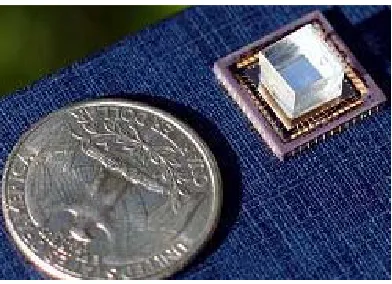
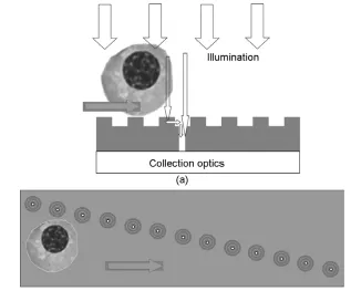
[image:43.612.212.408.318.460.2]Both microfluidics and nanoapertures are readily produced by making use of state-of-the-art planar fabrication technology. In our OFM implementation, we choose to fabricate the nanoaperture array based imager and the microfluidic chip separately. Then these two modules can be bonded together without having to overcome many technological obstacles. One example of a complete OFM is shown in Fig. 2-5 (by courtesy of Xiquan Cui); the total size is even smaller than a US quarter.
Figure 2-5: A compact OFM compared with a US quarter. The OFM consists of a CMOM camera, a thin metallic film with nanoaperture patterns and a microfluidic chip (by courtesy of Xiquan Cui).
Thus, the resolution of the resulting image by using this method cannot be better than the pixel size (L), i.e. 5 μm. (If over-sampling needs to be considered, then the resulting resolution should be 10 μm, i.e. 2L). Because the size of most of the cells is on the order of 10 μm, cells will show on the screen as featureless and hence tough-to-recognize objects. Therefore, we can conclude that this type of direct imaging, although simple and fast, has limited use in biology research.
However, we do not have to totally abandon this idea of direct projection imaging. One quick solution of its resolution problem is to make smaller camera pixels. For example, a camera with a pixel size of 200 nm will possibly give excellent resolution of a cell. There actually has been steady progress toward this direction, although the pace of the development is quite slow due to tremendous technological difficulties. Therefore, we need to seek new solutions before the pixel size of a CMOS camera can reach such a desired value.
In fact, we may see a slower-than-expected progress in the size reduction of CMOS camera from the semiconductor industry. The trade-off between the dynamic range of the camera pixels and the spatial resolution (i.e. the pixel size) of the camera makes it unfavorable to make the camera pixel too large or too small. Chen, T. and colleagues reported in their conference proceedings that [9], ‘for a typical O.35p CMOS technology the optimal pixel size is found to be approximately 6.5 μm at fill factor of 30%. It is shown that the optimal pixel size scales with technology, but at slower rate than the technology itself.’
(1) The first step of building an OFM
Optofluidic Microscope (OFM) successfully introduces the concept of nanoaperture imaging into this type of direct imaging scheme. More specifically, we make use of the OFM method to replace the camera pixels with nanoapertures that are much smaller.
the incoming photons. That is to say, we effectively reduce the size of each camera pixel during this fabrication procedure.
As was introduced in the previous section, the resolution of nanoaperture imaging is, in theory, limited only by the size of the aperture. Therefore, by defining tiny apertures on top of a metal-coated CMOS camera, we can dramatically improve the resolving power of a CMOS camera from the 10μm level to, possibly, the 100nm level.
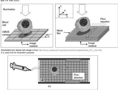
[image:45.612.134.512.308.597.2]Nevertheless, using such an imaging device is unlike using a CMOS camera, which can give a full field image within a few milliseconds. In the first-step OFM (Fig. 2-6(b, c)), the tiny apertures are not continually connected, which requires that we should scan the sample or scan the underlying imager, so that each nanoaperture can take a line scan over one stripe of the cell.
There are many methods of transporting cell samples, such as microfluidics, optical tweezers or magnetic tweezers. Within microfluidics, numerous actuation mechanisms can be employed, including pressure-difference, electrokinetics, magnetic force, etc. In Fig. 2-6(c), we show the bull’s eye view of the device, where a syringe pump is used to deliver the cell sample over the line of nanoapertures.
Nevertheless, we shall notice that there is an under-sampling issue associated with this imaging method. Although the nanoapertures take fine line-scans of the sample in x direction, they are not able to do so in y direction. The reason is that in y direction, these nanoapertures are supposed to separate from each other by at least the length of a camera pixel (~5 μm), such that no two nanoapertures will lie on the same camera pixel. This restriction on aperture spacing determines that the line scans of Fig. 2-6 (c) cannot overlap with each other - a requirement for sufficient sampling.
More specifically, in order to realize the desired optical resolution, it is required that the line scans from adjacent holes should separate from each other by no more than half the diameter of the nanoapertures. Therefore, we have to seek a different scanning scheme is in order to achieve the abovementioned condition of sufficient sampling.
(2) The second step of building an OFM
One proposed OFM design can perfectly overcome such an under-sampling issue. It is illustrated in Fig. 2-7(a) and was first outlined in Ref. [10].
although we still use the layout in Fig. 2-7 (a) to explain the key design parameters of OFM.
(a)
L
Flow direction
Nanoaperture orientation y
(b)
Nanoaperture orientation
[image:47.612.148.498.167.437.2]Flow direction
Figure 2-7: Two designs of OFM. (a) The nanoaperture array is punched in a slanted fashion on the CMOS camera; the microfluidic channel is aligned with the camera. (b) The nanoapertures are punched at the center of each camera pixel; the microfluidic channel is aligned in a slanted fashion.
We can easily calculate the pixel size (x, y) associated with this skewed scanning method:
(2.2) ) sin(T G
G G
L y
t v x
angle is fully controlled by the designer, and it can be adequately small as desired for a small y. On the other hand, the velocity of the sample motion can be as slow as 100’s of microns per second in microfluidics, and it can be even less than 1 μm/s by using other means, like optical tweezers. As such, with a high-speed CMOS camera (normally >5 KHz), x can also be made sufficiently small in order to satisfy the over-sampling conditions.
[image:48.612.128.520.374.603.2]Since the nanoapertures are laid out in a slanted fashion, the adjacent nanoapertures, e.g. Hole A and Hole B in Fig. 2-8(a), although scan the neighboring portions of the cell, do not actually ‘see’ the cell pass by at the same time. Such a result applies to all the other apertures inside the aperture array. As such, the time-of-flight line traces obtained from each aperture will inevitably have a time delay (t) with each other, as is illustrated in Fig. 2-8(b). If stacking together all the time traces in y direction, we will end up with a geometrically distorted image of an originally spherical cell (Fig. 2-8(c)).
Fortunately, this type of geometric distortion is not random and thus can be removed, assuming that the camera speed and the moving speed of the cell are both constant for the time when the target object passes through the nanoaperture array. By assuming that, we can obtain an expression for the time delay t as:
(2.3) cos
v L
t T
'
Note that both L and can be determined by fabrication or alignment. The sample speed v
is determined by the specific experimental conditions and thus has to be measured in real time.
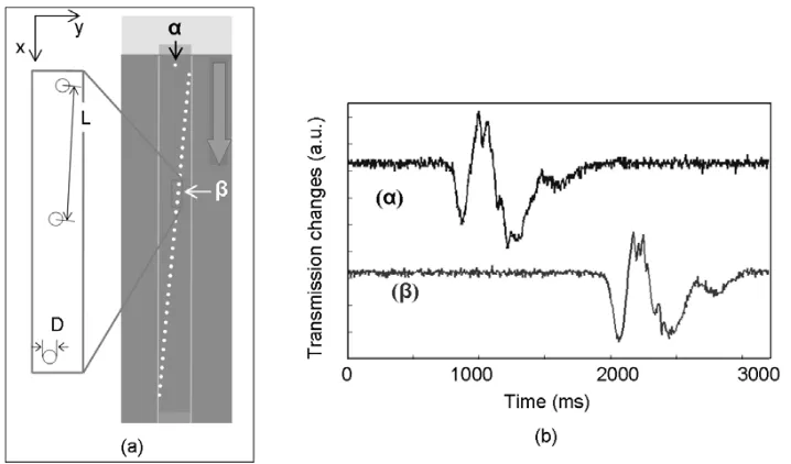
[image:49.612.142.501.406.617.2]A simple nanoaperture array is not able to measure the sample speed, as no nanoapertures can scan the identical parts of the object. However, v can be measured by adopting such a method as shown in Fig. 2-9(a). In this innovative design, v is measured through the use of an isolated aperture () at one end of the array, such as at the front end (Fig. 2-9(a)).
When we align the nanoaperture array with the fluidic channel in such way that aperture resides at the center of the channel, then the middle hole of the long nanoaperture array, i.e. aperture , will have the same y coordinate, as should scan the same line across the target. As such, v can be calculated as the ratio between the separation of these two apertures (DE ) by the time delay between them. After knowing the sample velocity v, then all the parameters in Eq. (2.2) and Eq. (2.3) can be immediately obtained.
In addition, this aperture pair serves an additional function – to monitor the possibility of tumbling/rotation of the pass-by targets. The line scans through different portions of the objects usually look very distinctive, because the target objects, particularly a biological sample, have fine features associated with them. Hence, if the target rotated or tumbled during its passage over the nanoaperture array, the two line scans extracted from aperture and aperture would appear dissimilar as the aperture pair scanned different portions of the cell. This unique property of a nanoaperture pair enables us to screen out rotating targets effectively. Figure 2-9(b) shows such a pair of similar line scans acquired through the aperture pair during the passage of an un-rotated C. elegans.
This piece of “tumbling screener” should be particularly useful in an automatic imaging scenario, where all the line scans are very rapidly recorded by the underlying camera chip and then read by a computer. The tumbling screener can automatically make a judgment about whether or not the sample was passing the nanoaperture array with a constant speed and static orientation, and then tell the computer program whether to process the data of this sample or dump it immediately. In the other words, this method ingeniously eliminates the human intervention of the entire image acquisition/processing procedure, thus saving a large amount of labor and time.
Besides using an isolated aperture, another way of automatically measuring the sample speed is to use multiple nanoaperture arrays to acquire an image [11]. As long as the nanoaperture pairs like and can be spotted in such a multiple-line array, a similar method can be used to calculate the flow speed and/or screen out rotating samples.
![Figure 1-3: Examples of optofluidic sensing or imaging devices. (a) Micro-FACS. The appearance of fluorescence signals at the ‘detection window’ triggers the opening of [14]](https://thumb-us.123doks.com/thumbv2/123dok_us/8928110.965147/27.612.128.519.130.388/figure-examples-optofluidic-sensing-appearance-fluorescence-detection-triggers.webp)