AA-AE36A-TV
TM
Color/Graphics Option
Programmer's Reference Guide
First Printing, June 1984
© Digital Equipment Corporation 1984. All Rights Reserved.
The information in this document is subject to change without notice and should not be construed as a commitment by Digital Equipment Corporation. Digital Equipment Corporation assumes no responsibility for any errors that may appear in this document.
The software described in this document is furnished under a license and may only be used or copied in accordance with the terms of such license.
No responsibility is assumed for the use or reliability of software on equipment that is not supplied by DIGITAL or its affiliated companies.
CP/M and CP/M-86 are registered trademarks of Digital Research Inc. CP/M-8O is a trademark of Digital Research Inc.
uPD7220 is a registered trademark of NEC Electronics U.S.A. Inc. 8088 is a registered trademark of Intel Corporation.
The following are trademarks of Digital Equipment Corporation:
~D~DDmD'"
DEC DECmate DECsystem-10 DECSYSTEM-20 DECUS
DECwriter DIBOL
MASSBUS PDP
P/OS
Professional Rainbow RSTS RSX
UNIBUS VAX VMS
VT
Work Processor
The postage-prepaid READER'S COMMENTS form on the last page of this document requests the user's critical evaluation to assist us in preparing future documentation.
Preface vii
The Intended Audience vii
Organization of the Manual vii
Suggestions for the Reader viii
PART I -
Operating Principles
Chapter 1. Overview 1-1
Hardware Components
1-1
Resolution Modes
1-3
Operational Modes
1-3
Chapter 2. Monitor Configurations 2-1
Monochrome Monitor Only
2-2
Color Monitor Only
2-3
Dual Monitors 2-4
Chapter 3. Graphics Option Logic 3-1
General
3-1
Data Logic
3-2
Address Logic
3-2
Display Logic
3-6
GDC Command Logic
3-9
Contents
Contents
Chapter 4. Graphics Option Components 4-1
I/O Ports
4-
1
Indirect Register
4-2
Write Buffer
4-2
Write Mask Registers
4-4
Pattern Generator
4-5
Foreground/Background Register
4-6
ALU/PS Register
4-8
Color Map
4-9
Mode Register
4-
15
Scroll Map
4-16
PART II -
Programming Guidelines
Chapter 5. Initialization and Control 5-1
T est for Option Present
5-
1
Test for Motherboard Version
5-2
Initialize the Graphics Option
5-6
Controlling Graphics Output
5-24
Modifying and Loading the Color Map
5-25
Chapter 6. Bitmap Write Setup (General) 6-1
Loading the ALU/PS Register
6-1
Loading the Foreground/Background Register
6-2
Chapter 7. Area Write Operations 7-1
Display Data from Memory
7-1
Set a Rectangular Area to a Color
7-4
Chapter 8. Vector Write Operations 8-1
Setting Up the Pattern Generator
8-1
Display a Pixel
8-4
Display a Vector
8-5
Display a Circle
8-9
Chapter 9. Text Write Operations 9-1
Write a Byte-Aligned Character
9-
1
Define and Position the Cursor
9-32
Write a Text String
9-38
Chapter 10. Read Operations 10-1
The Read Process
1 0- 1
Read the Entire Bitmap
10-1
Pixel Write After a Read Operation
1
0-5
Chapter 1 1. Scroll Operations 1 1-1
Vertical Scrolling
11-1
Horizontal Scrolling
11-4
Chapter 12. Programming Notes 12-1
Shadow Areas
12-1
Bitmap Refresh
12-1
Software Reset
12-2
Setting Up Clock Interrupts
12-2
Operational Requirements
12-3
Set-Up Mode
12-3
Timing Considerations
1
2-4
PART III -
Reference Material
Chapter 13. Option Registers, Buffers, and Maps 13-1
I/O Ports
1
3-
1
Indirect Register
1
3-3
Write Buffer
1
3-4
Write Mask Registers
1
3-5
Pattern Register
1
3-6
Pattern Multiplier
13-7
Foreground/Background Register
1
3-8
ALU/PS Register
13-9
Color Map
1 3-10
Mode Register
13-11
Scroll Map
13-12
Chapter 14. GDC Registers and Buffers
14-1
Status Register
14-1
FIFO Buffer
14-2
Chapter 15. GDC Commands 15- 1
Introduction
15-1
Video Control Commands
15-2
Display Control Commands
15-8
Drawing Control Commands
15-
1 3
Data Read Commands
15-1
8
Contents
Contents
PART IV -
Appendixes
Appendix A. Option Specification Summary A-1
Physical Specifications A- 1
Environmental Specifications A-1
Power Requirements A-2
Standards and Regulations
A-2
Part and Kit Numbers A-3
Appendix B. Rainbow Graphics Option -
Block Diagram B-1
Appendix C. Getting Help C-1
Index 1-1
Figures
Figure 1. Monochrome Monitor Only System
2-2
Figure 2. Color Monitor Only System
2-3
Figure 3. Dual Monitor System
2-4
Figure 4. Rows and Columns in Display Memory 3-3
Figure 5. Relationship of Display Memory to Address Logic
3-4
Figure 6. GDC Screen Control Parameters
3-8
Figure 7. Write Buffer as Accessed by the CPU and the GDC 4-3
Figure 8. Write Mask ReGISters
4-4
Figure 9. Pattern Generator 4-5
Figure 10. Foreground/Background ReGISter 4-7
Figure 11. Bitmap/Color Map Interaction (medium resolution)
4-10
Figure 12. Bitmap/Color Map Interaction (high resolution) 4-11
Figure 13. Sample Color Map with Loading Sequence 4-12
Figure 14. Scroll Map Operation 4-16
Figure 15. Rainbow Graphics Option -
Block Diagram B-3
Tables
vi
Table 1. Colors and Monochrome Intensities -
Displayed/Available
1-1
Table 2. Intensity Values vs Video Drive Voltages 4-14
Preface
The Intended Audience
The Rainbow Color/Graphics Option Programmer's Reference Guide is written for the experienced
systems programmer who will be programming applications that display graphics on Rainbow video
monitors.
It
is further assumed that the system programmer has had both graphics and 8088
pro-gramming experience.
The information contained in this document is not unique to any operating system; however, it is
specific to the 8088 hardware and 8088-based software.
Organization of the manual
The Rainbow Color/Graphics Option Programmer's Reference Guide is subdivided into four parts
containing fifteen chapters and three appendixes as follows:
• PART I -
OPERATING PRINCIPLES contains the following four chapters:
-
Chapter 1 provides an overview of the Graphics Option including information on the
hard-ware, logical interface to the CPU, general functionality, color and monochrome ranges, and
model dependencies.
-
Chapter 2 describes the monitor configurations supported by the Graphics Option.
Preface
-
Chapter 3 discusses the logic of data generation, bitmap addressing, and the GDC's handling
of the screen display.
-
Chapter 4 describes the software components of the Graphics Option such as the control
registers, maps, and buffer areas accessible under program control.
• PART II -
PROGRAMMING GUIDELINES contains the following eight chapters:
-
Chapter 5 discusses programming the Graphics Option for initialization and control
operations.
-
Chapter 6 discusses programming the Graphics Option for setting up bitmap write
operations.
-
Chapter 7 discusses programming the Graphics Option for area write operations.
-
Chapter 8 discusses programming the Graphics Option for vector write operations.
-
Chapter 9 discusses programming the Graphics Option for text write operations.
-
Chapter 10 discusses programming the Graphics Option for read operations.
-
Chapter 11 discusses programming the Graphics Option for scroll operations.
-
Chapter 12 contains programming notes and timing considerations.
• PART III -
REFERENCE MATERIAL contains the following three chapters:
-
Chapter 13 provides descriptions and contents of the Graphics Option's registers, buffers,
masks, and maps.
-
Chapter 14 provides descriptions and contents of the GDC's status register and FIFO buffer.
-
Chapter 15 provides a description of each supported GDC command arranged in alphabetic
sequence within functional grouping.
• PART IV -
APPENDIXES contain the following three appendixes:
-
Appendix A contains the Graphics Option's Specification Summary.
-
Appendix B is a fold-out sheet containing a block diagram of the Graphics Option.
-
Appendix C lists DIGITAL's International Help Line phone numbers.
Suggestions for the Reader
For more information about the Graphics Display Controller refer to the following:
• uPD7220 CDC Design Manual-NEC
Electronics U.S.A. Inc.
• uPD7220 CDC Design SPecification-NEC
Electronics U.S.A. Inc.
)
Preface
For a comprehensive tutorial/reference manual on computer graphics, consider
Fundamentals of
Interactive Computer Graphics by
J.
D. Foley and A. Van Dam published by Addison-Wesley
Publish-ing Company, 1982.
Terminology
ALU/pS
Bitmap
GDC
Motherboard
Nibble
Pixel
Resolution
RGB
RGO
RMW
VSS
Arithmetic Logical Unit and Plane Select (register)
Video display memory
Graphics. Display Controller
A term used to refer to the main circuit board where the processors and main
memory are located -
hardware options, such as the Graphics Option, plug
into and communicate with the motherboard
A term commonly used to refer to a half byte
(4
bits)
Picture element when referring to video display output
A measure of the sharpness of a graphics image -
usually given as the
number of addressable picture elements for some unit of length (pixels per
inch)
Red, green, blue -
the acronym for the primary additive colors used in color
monitor displays
Rainbow Graphics Option
Read/Modify/Write, the action taken when accessing the bitmap during a write
or read cycle
Video Subsystem
\
/PART I
Chapter 1. Overview 1-1
Hardware Components 1-1
Video Memory (Bitmap)
1-2
Additional Hardware
1-2
Resolution Modes
1-3
Medium Resolution Mode 1-3
High Resolution Mode 1-3
Operational Modes
1 -3
Chapter 2. Monitor Configurations 2-1
Monochrome Monitor Only 2-2
Color Monitor Only 2-3
Dual Monitors 2-4
Chapter 3. Graphics Option Logic 3-1
General 3-1
Data Logic 3-2
Address Logic 3-2
Display Logic 3-6
Bitmap Logic 3-6
Screen Logic
3-7
GDC Command Logic 3-9
Contents
Chapter 4. Graphics Option Components 4-1
I/O Ports
4- 1
Indirect Register 4-2
Write Buffer 4-2
Write Mask Registers
4-4
Pattern Generator 4-5
Foreground/Background Register 4-6
ALU/PS Register 4-8
Color Map 4-9
Loading the Color Map 4-12
Video Drive Voltages 4-13
Mode Register 4- 15
Scroll Map 4-16
1
Overview
Hardware Components
The Graphics Option is a user-installable module that adds graphics and color display capabilities to
the Rainbow system. The graphics module is based on a NEC uPD7220 Graphics Display Controller
(GDC) and an 8 X 64K dynamic RAM video memory that is also referred to as the bitmap.
The Graphics Option is supported, with minor differences, on Rainbow systems with either the model
A or model B motherboard. The differences involve the number of colors and monochrome
intensi-ties that can be simultaneously displayed and the number of colors and monochrome intensiintensi-ties that
are available to be displayed (see Table 1). Chapter 5 includes a programming example of how you
can determine which model of the motherboard is present in your system.
Table
1.
Colors and Monochrome Intensities -
Displayed/Available
MED. RESOLUTION HIGH RESOLUTION CONFIG. MODEL COLOR MONO. COLOR MONO. MONOCHROME 100-A N/A 4/4 N/A 4/4 MONITOR
ONLY 100-8 N/A 16/16 N/A 4/16 COLOR 100-A 16/1024 N/A 4/1024 N/A MONITOR
ONLY 100-8 16/4096 N/A 4/4096 N/A
DUAL 100-A 16/4096 4/4 4/4096 4/4 MONITORS
100-8 16/4096 16/16 4/4096 4/16
LJ-0212
[image:15.620.48.544.412.699.2]Overview
The GDC, in addition to performing the housekeeping chores for the video display, can also:
• Draw lines at any angle
• Draw arcs of specified radii and length
• Fill rectangular areas
• Transfer character bit-patterns from font tables in main memory to the bitmap
Video Memory (Bitmap)
The CPUs on the motherboard have no direct access to the bitmap memory. All writes are
per-formed by the external graphics option hardware to bitmap addresses generated by the GDC.
The bitmap is composed of eight 64K dynamic RAMs. This gives the bitmap a total of 8 X 64K of
display memory. In high resolution mode, this memory is configured as two planes, each 8 X 32K.
In medium resolution mode, this memory is configured as four planes, each 8 X 16K. However, as
far as the GDC is concerned, there is only one plane. All plane interaction is transparent to the GDC.
Although the bitmap is made up of 8 X 64K bits, the GDC sees only 16K of word addresses in high
resolution mode (2 planes X 16 bits X 16K words). Similarly, the GDC sees only 8K of word
addresses in medium resolution mode (4 planes X 16 bits X 8K words). Bitmap address zero is
displayed at the upper left corner of the monitor screen.
Additional Hardware
The option module also contains additional hardware that enhances the performance and versatility of
the GDC. This additional hardware includes:
• A 16 X 8-bit Write Buffer used to store byte-aligned or word-aligned characters for high
performance text writing or for fast block data moves from main memory to the bitmap
• An 8-bit Pattern Register and a 4-bit Pattern Multiplier for improved vector writing
performance
• Address offset hardware (256 X 8-bit Scroll Map) for full and split-screen vertical scrolling
• ALU/pS register to handle bitplane selection and the write functions of Replace, Complement,
and Overlay
• A 16 X 16-bit Color Map to provide easy manipulation of pixel color and monochrome
intensities
• Readback hardware for reading a selected bitmap memory plane into main memory
Overview
Resolution Modes
The Graphics Option operates in either of two resolution modes:
• Medium Resolution Mode
• High Resolution Mode
Medium Resolution Mode
Medium resolution mode displays 384 pixels horizontally by 240 pixels vertically by four bitmap
memory planes deep. This resolution mode allows up to 16 colors to be simultaneously displayed on a
color monitor. Up to sixteen monochrome shades can be displayed simultaneously on a monochrome
monitor.
High Resolution Mode
High resolution mode displays 800 pixels horizontally by 240 pixels vertically by two bitmap memory
planes deep. This mode allows up to four colors to be simultaneously displayed on a color monitor.
Up to four monochrome shades can be simultaneously displayed on a monochrome monitor.
Operational Modes
The Graphics Option supports the following modes of operations:
• WORD MODE to write 16-bit words to selected planes of the bitmap memory for character and
image generation
• VECTOR MODE to write pixel data to bitmap addresses provided by the GDC
• SCROLL MODE for full- and split-screen vertical scrolling and full-screen horizontal scrolling
• READBACK MODE to read 16-bit words from a selected plane of bitmap memory for special
applications, hardcopy generation or diagnostic purposes
2
Monitor Configurations
In the Rainbow system with the Graphics Option installed, there are three possible monitor
configu-rations: Monochrome only, Color only, and Dual (color and monochrome). In all three configurations,
the selection of the option's monochrome output or the motherboard VTI02 video output is
con-trolled by bit two of the system maintenance port (port OAh). A 0 in bit 2 selects the motherboard
VTI02 video output while a 1 in bit 2 selects the option's monochrome output.
Monitor Configurations
Monochrome Monitor Only
As shown in Figure 1, the monochrome monitor can display either graphics option data or
motherboard data depending on the setting of bit 2 of port OAh. Writing an 87h to port OAh selects
the Graphics Option data. Writing an 83h to port OAh selects the motherboard VT102 data. The red,
green and blue data areas in the Color Map should be loaded with all F's to reduce any unnecessary
radio frequency emissions.
BLUE INTENSITIES
RED INTENSITIES
GREEN INTENSITIES
MONOCHROME INTENSITIES---4"
~---... MONOCHROME MONITOR
MOTHERBOARD D A T A - - - - -...
PORT OAh (BIT 2)---~
LJ-0215
Figure 1. Monochrome Monitor Only System
2-2
(
[image:20.627.113.504.227.386.2]Monitor Configurations
Color Monitor Only
When the system is configured with only a color monitor, as in Figure 2, the green gun does double
duty.
It
either displays the green component of the graphics output or it displays the monochrome
output of the motherboard VT102 video subsystem. Because the green gun takes monochrome
intensities, all green intensities must be programmed into the monochrome data area of the Color
Map. The green data area of the Color Map should be loaded with all F's to reduce any unnecessary
radio frequency emissions.
BLUE INTENSITIES ---~~BLUEGUN RED I NTENSITI ES - - - -... ~ RED GU N GREEN INTENSITIES
MONOCHROME INTENSITIES ~
(GREEN DATA)
) - - - - . GREEN GUN MOTHERBOARD DATA---1~
PORT OAh (BIT 2)
LJ-0216
Figure 2. Color Monitor Only System
When motherboard VT102 data is being sent to the green gun, the red and blue output must be
turned off at the Graphics Option itself.
If
not, the red and blue guns will continue to receive data
from the option and this output will overlay the motherboard VT102 data and will also be out of
synchronization. Bit 7 of the Mode Register is the graphics option output enable bit.
If
this bit is a 1
red and blue outputs are enabled.
If
this bit is a 0 red and blue outputs are disabled.
As in the monochrome only configuration, bit 2 of port OAh controls the selection of either the
graphics option data or the motherboard VT102 data. Writing an 87h to port OAh enables the option
data. Writing an 83h to port OAh selects the motherboard VT102 data.
[image:21.623.160.456.230.387.2]Monitor Configurations
Dual Monitors
In the configuration shown in Figure 3, both a color monitor and a monochrome monitor are available
to the system. Motherboard VTI02 video data can be displayed on the monochrome system while
color graphics are being displayed on the color monitor.
If
the need should arise to display graphics
on the monochrome monitor, the monochrome intensity output can be directed to the monochrome
monitor by writing an 87h to port OAh. Writing an 83h to port OAh will restore motherboard
VTI02 video output to the monochrome monitor.
BLUE INTENSITIES - - - -•• BLUE GUN RED INTENSITIES - - - . . RED GUN GREEN I N T E N S I T I E S - - - . . GREEN GUN MONOCHROME INTENSITIES --~.~
>---~ MONOCHROME MONITOR MOTHERBOARD DATA----~.~
PORT OAh (BIT 2 ) - - - J
LJ-0217
Figure 3. Dual Monitor System
When displaying graphics on the monochrome monitor, the only difference other than the the lack of
color is the range of intensities that can be simultaneously displayed on systems with model A
motherboards.
Systems with model A motherboards can display only four monochrome intensities at anyone time.
Even though sixteen entries can be selected when operating in medium resolution mode, only the
two low-order bits of the monochrome output are active. This limits the display to only four unique
intensities at most. On systems with the model B motherboard, all sixteen monochrome intensities
can be displayed.
[image:22.624.109.493.227.390.2]3
Graphics Option logic
General
The Graphics Display Controller (GDC) can operate either on one bit at a time or on an entire 16-bit
word at a time.
It
is, however, limited to one address space and therefore can only write into one
plane at a time. The Graphics Option is designed in such a manner that while the GDC is doing
single pixel operations on just one video plane, the external hardware can be doing 16-bit word
operations on up to four planes of video memory.
Write operations are multi-dimensioned. They have width, depth, length and time.
• Width refers to the number of pixels involved in the write operation.
• Depth refers to the number of planes involved in the write operation.
• Length refers to the number of read/modify/write cycles the GDC is programmed to perform.
• Time refers to when the write operation occurs in relation to the normal housekeeping
opera-tions the GDC has to perform in order to keep the monitor image stable and coherent.
Graphics Option Logic
Data Logic
The Graphics Option can write in two modes: word mode (16 bits at a time) and vector mode (one
pixel at a time).
In word mode, the data patterns to be written into the bitmap are based on bit patterns loaded into
the Write Buffer, Write Mask, and the Foreground/Background Register, along with the type of
write operation programmed into the ALU/PS Register.
In vector mode, the data patterns to be written to the bitmap are based on bit patterns loaded into
the Pattern Register, the Pattern Multiplier, the Foreground/Background Register, and the type of
write operation programmed into the ALU/PS Register.
In either case, the data will be stored in the bitmap at a location determined by the addressing logic.
Address Logic
The addressing logic of the Graphics Option is responsible for coming up with the plane, the line
within the plane, the word within the line, and even the pixel within the word under some conditions.
The display memory on the Graphics Option is one-dimensional. The GDC scans this linear memory
to generate the two dimensional display on the CRT. The video display is organized similarly to the
fourth quadrant of the Cartesian plane with the origin in the upper left corner. Row addresses (y
coordinates of pixels) start at zero and increase downwards while column addresses (x coordinates of
pixels) start at zero and increase to the right (see Figure 4). Pixel data is stored in display memory
by column within row.
Graphics Option Logic
COLUMN (X) ROW(Y!
°
2•
• •
NI
°
(0,0) (1,0) (2,0) (N,O) (0,1) (1,1) (2,1) (N,1 )2 (0,2) (1,2) (2,2) (N,2)
~
•
•
•
M (O,M) (1,M) (2,M) (N,M)
LJ-0218
Figure 4. Rows and Columns in Display Memory
The GDC accesses the display memory as a number of 16-bit words where each bit represents a
pixel. The number of words defined as well as the number of words displayed on each line is
dependent on the resolution. The relationship between words and display lines is shown in Figure 5.
[image:25.620.167.457.101.362.2]Graphics Option Logic
LINE 0
LINE 1
LINE 2
•
•
•
LINE N-l
3-4
""---
WORDS/LINE DEFINED---~~I
... I ..
t---
WORDS/LINE DISPLAYED---I~~I
0 1 2 Q-l P-l
P P+l P+2 P+Q-l 2P-l
2P 2P+l 2P+Q-l 3P-l
3P 3P+Q-l 4P-l
4P 4P+Q-l 5P-l
l,/ l,.;
(M-l )P MP-l
1N-1
1
PI
NP-lJ
WHERE:
P
=
WORDS/LINE DEFINED - 32 IN MEDIUM RESOLUTION. - 64 IN HIGH RESOLUTION.Q
=
WORDS/LINE DISPLAYED - 24 IN MEDIUM RESOLUTION - 50 IN HIGH RESOLUTIONN
=
NO. OF LINES DEFINED - 256M
=
NO. OF LINES DISPLAYED - 240LJ-0219
[image:26.624.81.540.74.672.2]Graphics Option Logic
In order to address specific pixels, the GDC requires the word address and the pixel location within
that word. The conversion of pixel coordinates to addresses in display memory is accomplished by
the following formulas:
Given the pixel coordinates (x,y):
Word Address of pixel
=
(words/line defined * y) + integer(x/16) Pixel Address within word = remainder(x/16)*
16Because the Graphics Option is a multi-plane device, a way is provided to selectively enable and
disable the reading and writing of the individual planes. This function is performed by the ALUjPS
and Mode registers. More than one plane at a time can be enabled for a write operation; however,
only one plane can be enabled for a read operation at anyone time.
The entire address generated by the GDC does not go directly to the bitmap. The low-order six bits
address a word within a line in the bitmap and do go directly to the bitmap. The high-order eight bits
address the line within the plane and these bits are used as address inputs to a Scroll Map. The
Scroll Map acts as a translator such that the bitmap location can be selectively shifted in units of 64
words. In high resolution mode, 64 words equate to one scan line; in medium resolution mode, they
equate to two scan lines. This allows the displayed vertical location of an image to be moved in
64-word increments without actually rewriting it to the bitmap. Programs using this feature can provide
full and split screen vertical scrolling. The Scroll Map is used in all bitmap access operations: writing,
reading, and refreshing.
If
an application requires addressing individual pixels within a word, the two 8-bit Write Mask
Registers can be used to provide a 16-bit mask that will write-enable selected pixels. Alternately, a
single pixel vector write operation can be used.
There is a difference between the number of words/line defined and the number of words/line
displayed. In medium resolution, each scan line is 32 words long but only 24 words are displayed (24
words
*
16 bits/word
=384 pixels). The eight words not displayed are unusable. Defining the length
of the scan line as 24 words would be a more efficient use of memory but it would take longer to
refresh the memory. Because display memory is organized as a 256 by 256 array, it takes 256 bytes
of scan to refresh the entire 64K byte memory. Defining the scan line length as 32 words long
enables the entire memory to be refreshed in four line scan periods. Defining the scan line length as
24 words long would require five line scans plus 16 bytes.
Similarly, in high resolution, each scan line is 64 words long but only 50 words are displayed. With a
64 word scan line length, it takes two line scan periods to refresh the entire 64K byte memory.
If
the scan line length were 50 words, it would take two lines plus 56 bytes to refresh the memory.
Another advantage to defining scan line length as 32 or 64 words is that cursor locating can be
accomplished by a series of shift instructions which are considerably faster than multiplying.
Graphics Option Logic
Display
logic
The display logic of the Graphics Option will be discussed as it applies to both the bitmap and the
screen.
Bitmap Logic
Data in the bitmap does not go directly to the monitor. Instead, the bitmap data is used as an
address into a Color Map. The output of this Color Map, which has been preloaded with color and
monochrome intensity values, is the data that is sent to the monitor.
In medium resolution mode there are four planes to the bitmap; each plane providing an address bit
to the Color Map. Four bits can address sixteen unique locations at most. This gives a maximum of
16 addressable Color Map entries. Each Color Map entry is 16 bits wide. Four of the bits are used
to drive the color monitor's red gun, four go to the green gun, four go to the blue gun, and four
drive the output to the monochrome monitor. In systems with the Model 100-A motherboard, only
the two low-order bits of the monochrome output are used. Therefore, although there are 16
possi-ble monochrome selections in the Color Map, the number of unique intensities that can be sent to
the monochrome monitor is four.
In high resolution mode there are two planes to the bitmap; each plane providing an address bit to
the Color Map. Two bits can address four entries in the Color Map at most. Again, each Color Map
entry is sixteen bits wide with 12 bits of information used for color and four used for monochrome
shades. In systems with the Model 100-A motherboard, only the two low-order bits of the
mono-chrome output are used. This limits the number of unique monomono-chrome intensities to four.
Although the Color Map is 16 bits wide, the color intensity values are loaded one byte at a time.
First, the 16 pairs of values representing the red and green intensities are loaded into bits 0 through
7 of the map. Then, the 16 pairs of values representing the blue and monochrome intensities are
loaded into bits 8 through 15 of the map.
Graphics Option Logic
Screen Logic
The image displayed on the screen is generated by an electron beam performing a series of
horizon-tal line scans from left to right. At the end of each horizonhorizon-tal scan line, a horizonhorizon-tal retrace takes
place at which time the electron beam reverses its horizontal direction. During this horizontal
retrace, the electron beam is also being moved down to the beginning of the next scan line. When
the last line has completed its horizontal retrace, a vertical retrace takes place at which time the
electron beam's vertical movement is reversed and the beam is positioned at the beginning of the
first scan line.
The
CDC
writes to the bitmap only during the screen's horizontal and vertical retrace periods.
During active screen time, the
CDC
is taking information out of the bitmap and presenting it to the
video screen hardware. For example, if the
CDC
is drawing a vector to the bitmap, it will stop
writing during active screen time and resume writing the vector at the next horizontal or vertical
retrace.
In
addition to the active screen time and the horizontal and vertical retrace times, there are several
other screen control parameters that precede and follow the active horizontal scans and active lines.
These are the Vertical Front and Back Porches and the Horizontal Front and Back Porches. The
relationship between the screen control parameters is shown in Figure 6. Taking all the parameters
into account, the proportion of active screen time to bitmap writing time is approximately four to
one.
Graphics Option Logic
3-8
GDC VIDEO CONTROL PARAMETERS
VERTICAL { FRONT PORCH
(3 LINES)
---~----~O~--- ~
~~O---~--- o DOD
ACTIVE DISPLAY
(240 LINES)
VERTICAL BACK PORCH
(16 LINES)
---~OO--- - - - -<l- - -
-
(J"'OO---~~-a---~~---~---- - - -0 0 0 0
---~---o 0 0 0
-
---~---~o-o---_+---
-O"Lj-o __ - - - < )
-o 0 0 .p
____ 4
-0"z:>-6- - - ___
-4--______
----<r"---~ClO---~~---+_---___ ----E2-0-~
-- ---- ---
---~-
---O"O-a -- ---
---:---(j~-O--- - - - ____ < 1
-O"cns--- - - - - <l
-o 0 0 0
--- -
---~----0" ~ -0
---:,...::'---+---
________ ~!l.Q.>J________
---<l---o 0 0 HORIZONTAL FRONT PORCH (WORDS)
o 0 0 HORIZONTAL BACK PORCH (WORDS)
-<l- - - HORIZONTAL RETRACE (WORDS)
_ HORIZONTAL ACTIVE (WORDS)
HIGH RESOLUTION
3
4
5
50
- HORIZONTAL INACTIVE (VERTICAL FRONT & BACK PORCHES)
VERTICAL RETRACE (LINES) 3
Figure 6. GDC Screen Control Parameters
MEDIUM RESOLUTION
3
2
24
[image:30.623.105.500.95.686.2]Graphics Option Logic
GDC Command logic
Commands are passed to the GDC command processor from the Rainbow system by writing
com-mand bytes to port 57h and parameter bytes to port 56h. Data written to these two ports is stored
in the GDC's FIFO buffer, a 16 x 9-bit area that is used to both read from and write to the GDC.
The FIFO buffer operates in half-duplex mode -
passing data in both directions, one direction at a
time. The direction of data flow at anyone time is controlled by GDC commands.
When commands are stored in the FIFO buffer, a flag bit is associated with each data byte depending
on whether the data byte was written to the command address (57h) or the parameter address (56h).
A flag bit of 1 denotes a command byte; a flag bit of 0 denotes a parameter byte. The command
processor tests this flag bit as it interprets the contents of the FIFO buffer.
The receipt of a command byte by the command processor signifies the end of the previous
com-mand and any associated parameters.
If
the command is one that requires a response from the GDC
such as RDAT, the FIFO buffer is automatically placed into read mode and the buffer direction is
reversed. The specified data from the bitmap is loaded into the FIFO buffer and can be accessed by
the system using read operations to port 57h. Any commands or parameters in the FIFO buffer that
follow the read command are lost when the FIFO buffer's direction is reversed.
When the FIFO buffer is in read mode, any command byte written to port 57h will immediately
terminate the read operation and reverse the buffer direction to write mode. Any data that has not
been read by the Rainbow system from the FIFO buffer will be lost.
(
"\
)
4
Graphics Option Components
I/O Ports
The CPUs on the Rainbow system's motherboard use a number of 8-bit I/O ports to exchange
information with the various subsystems and options. The I/O ports assigned to the Graphics Option
are ports 50h through 57h. They are used to generate and display graphic images, inquire status,
and read the contents of video memory (bitmap). The function of each of the Graphics Option's I/O
ports is as follows:
Port
Function
50h
Graphics option software reset. Any write to this port also resynchronizes the
read/modify/write memory cycles of the Graphics Option to those of the GDC.
5Ih
Data written to this port is loaded into the area selected by the previous write to port 53h.
52h
Data written to this port is loaded into the Write Buffer.
53h
Data written to this port provides address selection for indirect addressing (see Indirect
Register).
54h
Data written to this port is loaded into the low-order byte of the Write Mask.
55h
Data written to this port is loaded into the high-order byte of the Write Mask.
56h
Data written to this port is loaded into the GDC's FIFO Buffer and flagged as a parameter.
Data read from this port reflects the GDC status.
57h
Data written to this port is loaded into the GDC's FIFO Buffer and flagged as a command.
Data read from this port reflects information extracted from the bitmap.
Graphics Option Components
Indirect Register
The Graphics Option uses indirect addressing to enable it to address more registers and storage
areas on the option module than there are address lines (ports) to accommodate them. Indirect
addressing involves writing to two ports. A write to port 53h loads the Indirect Register with a bit
array in which each bit selects one of eight areas.
The Indirect Register bits and the corresponding areas are as follows:
Bit
Area Selected
0
Write Buffer
(*)1
Pattern Multiplier
2
Pattern Register
3
Foreground/Background Register
4
ALU/PS Register
5
Color Map
(*)6
Mode Register
7
Scroll Map
(*)(*)
Also clears the associated index counter
Mter selecting an area by writing to port 53h, you access and load data into most selected areas by
writing to port 51h. For the Write Buffer however, you need both a write of anything to port 51h to
access the buffer and clear the counter and then a write to port 52h to load the data.
Write Buffer
A 16 X 8-bit Write Buffer provides the data for the bitmap when the Graphics Option is in Word
Mode. You can use the buffer to transfer blocks of data from the system's memory to the bitmap.
The data can be full screen images of the bitmap or bit-pattern representations of font characters
that have been stored in motherboard memory. The buffer has an associated index counter that is
cleared when the Write Buffer is selected.
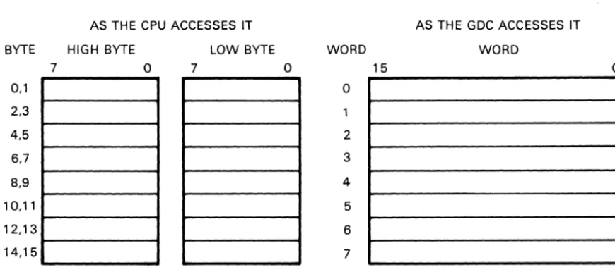
Although the CPU accesses the Write Buffer as sixteen 8-bit bytes, the GDC accesses the buffer as
eight 16-bit words. (See Figure 7.) A 16-bit Write Mask gives the GDC control over individual bits
of a word.
4-2
/
AS THE CPU ACCESSES IT BYTE HIGH BYTE
0,1
2,3
4,5
6,7
8,9
7
0
10,11
I---~ 12,13
I---~ 14,15
LOW BYTE
7
0
WORD
o
2
3
4
5
6
7 15
Graphics Option Components
AS THE GDC ACCESSES IT WORD
o
LJ-0221
Figure 7. Write Buffer as Accessed
by
the CPU and the GDC
The output of the Write Buffer is the inverse of its input.
If
a word is written into the buffer as
FFB6h, it will be read out of the buffer as 0049h. To have the same data written out to the bitmap
as was received from the CPU requires an added inversion step. You can exclusive or (XOR) the
CPU data with FFh to pre-invert the data before going through the Write Buffer. Alternately, you
can write zeros into the Foreground Register and ones into the Background Register to re-invert the
data after it leaves the Write Buffer and before it is written to the bitmap. Use one method or the
other, not both.
In order to load data into the Write Buffer, you first write an FEh to port 53h and any value to port
51h. This not only selects the Write Buffer but also sets the Write Buffer Index Counter to zero.
The data is then loaded into the buffer by writing it to port 52h in high-byte low-byte order.
If
more
than 16 bytes are written to the buffer the first 16 bytes will be overwritten.
If
you load the buffer with less than 16 bytes (or other than a multiple of 16 bytes for some reason
or other) the GDC will find an index value other than zero in the counter. Starting at a location other
than zero alters the data intended for the bitmap. Therefore, before the GDC is given the command
to write to the bitmap, you must again clear the Write Buffer Index Counter so that the GDC will
start accessing the data at word zero.
[image:35.627.84.519.96.294.2]Graphics Option Components
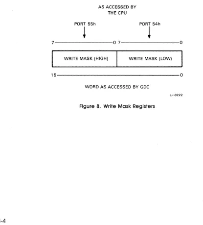
Write Mask Registers
When the Graphics Option is in Word Mode, bitmap operations are carried out in units of 16-bit
words. A 16-bit Write Mask controls the writing of individual bits within a word. A zero in a bit
position of the mask allows writing to the corresponding position of the word. A one in a bit position
of the mask disables writing to the corresponding position of the word.
While the GDC accesses the mask as a 16-bit word, the CPU accesses the mask as two of the
Graphic Option's I/O ports. The high-order Write Mask Register is loaded with a write to port 55h
and corresponds to bits 15 through 8 of the Write Mask. The low-order Write Mask Register is
loaded with a write to port 54h and corresponds to bits 7 through 0 of the Write Mask. (See Figure
8.)
4-4
PORT 55h
~
AS ACCESSED BY THE CPU
PORT 54h
~
7---0 7---0
WRITE MASK (HIGH) WRITE MASK (LOW)
15---0
WORD AS ACCESSED BY GDC
LJ-0222
[image:36.626.70.485.277.736.2]\
Graphics Option Components
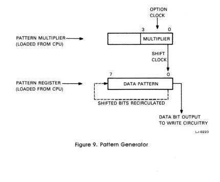
Pattern Generator
When the Graphics Option is in Vector Mode, the Pattern Generator provides the data to be written
to the bitmap. The Pattern Generator is composed of a Pattern Register and a Pattern Multiplier.
The Pattern Register is an 8-bit recirculating shift register that is first selected by writing FBh to
port 53h and then loaded by writing an 8-bit data pattern to port 5Ih.
The Pattern Multiplier is a 4-bit register that is first selected by writing FDh to port 53h and then
loaded by writing a value of O-Fh to port 5Ih.
NOTE
You must load the Pattern Multiplier before loading the Pattern Register.
Figure 9 shows the logic of the Pattern Generator. Data destined for the bitmap originates from the
low-order bit of the Pattern Register. That same bit continues to be the output until the Pattern
Register is shifted. When the most significant bit of the Pattern Register has completed its output
cycle, the next bit to shift out will be the least significant bit again.
PATTERN MULTIPLlER----., ... (LOADED FROM CPU)
PATTERN REGISTER
---I."
(LOADED FROM CPU)3
OPTION CLOCK
~
o
MULTIPLIER7
SHIFT CLOCK
1-- DATA PATTERN
I
o
I
IL _ _ _ _ _ _ _ _ _ _ _ _ _ _ _ _ _ _ _ I
SHIFTED BITS RECIRCULATED
DATA BIT OUTPUT TO WRITE CIRCUITRY
LJ-0223
Figure 9. Pattern Generator
[image:37.627.98.529.356.712.2]Graphics Option Components
The shift frequency is the write frequency from the option clock divided by 16 minus the value in
the Pattern Multiplier. For example, if the value in the Pattern Multiplier is 12, the shift frequency
divisor would be 16 minus 12 or four. The shift frequency would be one fourth of the write
fre-quency and therefore each bit in the Pattern Register would be replicated in the output stream four
times. A multiplier of 15 would take 16 - 15 or one write cycle for each Pattern Register bit shifted
out. A multiplier of five would take 16 - 5 or 11 write cycles for each bit in the Pattern Register.
NOTE
Do not change the contents of the Pattern Multiplier or the Pattern
Regis-ter before the GDC has completed all pending vector mode write
opera-tions.
If
you do, the vector pattern that is in the process of being displayed
will take on the new characteristics of the Pattern Generator.
Foreground/Background Register
The Foreground/Background Register is an eight-bit write-only register. The high-order nibble is the
Foreground Register; the low-order nibble is the Background Register. Each of the four bitmap
planes has a Foreground/Background bit-pair associated with it (see Figure 10). The bit settings in
the Foreground/Background Register, along with the mode specified in the ALU/PS Register,
deter-mine the data that is eventually received by the bitmap. For example; if the mode is REPLACE, an
incoming data bit of 0 is replaced by the corresponding bit in the Background Register.
If
the
incoming data bit is a 1, the bit would be replaced by the corresponding bit in the Foreground
Register.
Each bitmap plane has its own individual Foreground/Background bit pair. Therefore, it is possible
for two enabled planes to use the same incoming data pattern and end up with different bitmap
patterns.
Graphics Option Components
NOTE
3
FOREGROUND REGISTER
2 1 0
PLANE 0 PLANE 1 PLANE 2
PLANE 3
3
1
BACKGROUND REGISTER
2 1
01
0
LJ-0224
Figure 10. Foreground/Background Register
Do not change the contents of the Foreground/Background Register before
the GDC has completed all pending write operations.
If
you do, the
informa-tion that is in the process of being displayed will take on the new values of
the Foreground/Background Register.
[image:39.624.169.438.98.354.2]Graphics Option Components
ALU
IPS
Register
The ALUjPS Register has two functions.
Bits
°
through 3 of the ALUjPS Register are used to inhibit writes to one or more of the bitmap
planes.
If
you could not inhibit writes to the bitmap planes, each write operation would affect all
available planes. When a plane select bit is set to 1, writes to that plane will be inhibited. When a
plane select bit is set to 0, writes to that plane will be allowed.
NOTE
During a readback mode operation, all plane select bits should be set to
ones to prevent accidental changes to the bitmap data.
Bits 4 and 5 of the ALU/PS Register define an arithmetic logic unit function. The three logic
functions supported by the option are REPLACE, COMPLEMENT, and OVERLAY. These functions
operate on the incoming data from the Write Buffer or the Pattern Generator as modified by the
Foreground/Background Register as well as the current data in the bitmap and generate the new
data to be placed into the bitmap.
When the logic unit is operating in REPLACE mode, the current data in the bitmap is replaced by
the Foreground/Background data selected as follows:
• An
incoming data bit
°
selects the Background data.
• An incoming data bit 1 selects the Foreground data.
When the logic unit is operating in COMPLEMENT mode, the current data in the bitmap is modified
as follows:
• An incoming data bit
°
results in no change.
• An incoming data bit 1 results in the current data being exclusively or'ed (XOR) with the
appropriate Foreground bit.
If
the Foreground bit is 0, the current data is unchanged.
If
the
Foreground bit is 1, the current data is complemented by binary inversion. In effect, the
Foreground Register acts as a plane select register for the complement operation.
Graphics Option Components
When the logic unit is operating in OVERLAY mode, the current data in the bitmap is modified as
follows:
• An incoming data bit 0 results in no change.
• An incoming data bit 1 results in the current data being replaced by the appropriate Foreground
bit.
NOTE
Do not change the contents of the ALU
IPS
Register before the GDC has
completed all pending write operations.
If
you do, the information that is in
the process of being displayed will take on the new characteristics of the
ALU/PS Register.
Color Map
The Color Map is a 16 X 16-bit RAM area where each of the 16 entries is composed of four 4-bit
values representing color intensities. These values represent, from high order to low order, the
monochrome, blue, red, and green outputs to the video monitor. Intensity values are specified in
inverse logic. At one extreme, a value of zero represents maximum intensity (100% output) for a
particular color or monochrome shade. At the other extreme, a value of OFh represents minimum
intensity (zero output).
Bitmap data is not directly displayed on the monitor, each bitmap plane contributes one bit to an
index into the Color Map. The output of the Color Map is the data that is passed to the monitor.
Four bitmap planes (medium resolution) provide four bits to form an index allowing up to 16
intensi-ties of color or monochrome to be simultaneously displayed on the monitor. Two bitmap planes (high
resolution) provide two bits to form an index allowing only four intensities of color or monochrome to
be simultaneously displayed on the monitor.
Graphics Option Components
In Figure 11, a medium resolution configuration, the bitmap data for the display point x,y is 0110b.
This value, when applied as an index into the Color Map, selects the seventh entry out of a possible
sixteen. Each Color Map entry is sixteen bits wide. Four of the bits are used to drive the color
monitor's red gun, four go to the green gun, four go to the blue gun, and four drive the output to
the monochrome monitor. The twelve bits going to the color monitor support a color palette of 4096
colors; the four bits to the monochrome monitor support 16 shades. (In systems with the Model
100-A motherboard, only the two low-order bits of the monochrome output are active. This limits the
monochrome output to four unique intensities.)
4-10
BITMAP /
/
PLANE 0 0 BITMAP DATA
/
/
I
PLANE 1 1 0110b
/
PLANE 2 1/
I
/
/ PLANE 3 0
I
X,Y
4(*) BITS OF MONOCHROME LEVEL TO MONO. MONITOR 4 BITS OF BLUE LEVEL TO COLOR MONITOR 4 BITS OF RED LEVEL TO COLOR MONITOR 4 BITS OF GREEN LEVEL TO COLOR MONITOR
(*) 2 LOW-ORDER BITS ON MODEL 100-A SYSTEMS
COLOR MAP
0
•
•
•
•
6•
•
•
•
•
15
-LJ-0225
[image:42.623.105.506.220.434.2]Graphics Option Components
In Figure 12, a high resolution configuration, the bitmap data for point (x,y) is lOb. This value, when
applied as an index into the Color Map, selects the third entry out of a possible four. Again, each
Color Map entry is sixteen bits wide; 12 bits of information are used for color and four are used for
monochrome. (In systems with the Model 100-A motherboard, only the two low-order bits of the
monochrome output are active. This limits the monochrome output to four unique intensities.)
BITMAP PLANE
a
PLANE 1
I
,1
I
I
(X,Y)
I I
/
a
I/
BITMAP DATA
4(*) BITS OF MONOCHROME LEVEL TO MONO. MONITOR 4 BITS OF BLUE LEVEL TO COLOR MONITOR 4 BITS OF RED LEVEL TO COLOR MONITOR 4 BITS OF GREEN LEVEL TO COLOR MONITOR
(*) 2 LOW-ORDER BITS ON MODEL 100-A SYSTEMS
a
1 ~ 2 3
•
•
•
15Figure 12. Bitmap/Color Map Interaction (high resolution)
COLOR MAP
LJ-0226
[image:43.612.172.517.192.406.2]Graphics Option Components
Loading the Color Map
The Graphics Option accesses the Color Map as sixteen 16-bit words. However, the CPU accesses
the Color Map as 32 eight-bit bytes. The 32 bytes of intensity values are loaded into the Color Map
one entire column of 16 bytes at a time. The red and green values are always loaded first, then the
monochrome and blue values. (See Figure 13.)
4-12
ADDRESS VALUE
o
2
3
4
5
6
•
•
•
•
15
7
i.-'
1
2ND 16 BYTES 1ST 16 BYTES LOADED BY LOADED BY
THE CPU THE CPU 4 3
o
7 4 3 0MONO. BLUE RED GREEN COLOR MONOCHROME DATA DATA DATA DATA DISPLAYED DISPLAYED
15 15 15 15 BLACK BLACK
•
14 15 0 15 RED
•
•
13 15 15 0 GREEN GR 12 0 15 15 BLUE
A 11 0 0 15 MAGENTA Y S 10 0 15 0 CYAN H A
9 15 0 0 YELLOW D E
V
o
o
o
o
1
•
S•
•
•
•
•
•
WHITE WHITE
LJ-0227
[image:44.613.102.531.205.546.2]\
Graphics Option Components
Writing the value DFh to port S3h selects the Color Map and also clears the Color Map Index
Counter to zero. To load data into the Color Map requires writing to port Slh. Each write to port
Slh will cause whatever is on the motherboard data bus to be loaded into the current Color Map
location. After each write, the Color Map Index Counter is incremented by one.
If
33 writes are
made to the Color Map, the first Color Map location will be overwritten.
NOTE
Do not change the contents of the Color Map before the GDC has
com-pleted all pending write operations.
If
you do, the information that is in the
process of being displayed will take on the new Color Map characteristics.
Video Drive Voltages
The output of the Color Map, as shown in Figures 11 and 12, consists of four 4-bit values that
represent the red, green, blue, and monochrome intensities to be displayed on some applicable
monitor. These four intensity values are the input to four digital-to-analog converters. (Refer to the
block diagram in Appendix
B.) The output of these converters are the video drive voltages that are
applied to pins 9 through 12 of the J3 Video Output Jack.
The output of the digital-to-analog converters for the red, green, and blue intensities is not
depen-dent on the model of the system motherboard. The digital-to-analog converter for the monochrome
intensities, however, produces different output depending on whether the motherboard is a model A
or a model
B. On systems with a model A motherboard, only the two low-order bits of the intensity
value are active. This provides a limited range of only four output voltages for the m()nochrome
signal. On a color monitor only configuration, where the green output is derived from the
mono-chrome portion of the Color Map, the same limited range applies. On systems with a model B
motherboard, all four bits of the intensity value are active. This provides the full range of 16 output
voltages for the red, green, blue, and monochrome signals. The conversion of Color Map intensity
values to video drive voltages for each of these ranges are shown in Table 2.
The perceived intensity of a display is not linearly related to the video drive voltages. A given
difference in drive voltage at the high end of the range is not as noticeable as the same difference
occurring at the low end of the range.
Graphics Option Components
Table 2. Intensity Values vs Video Drive Voltages
INTENSITY VALUES VIDEO DRIVE VOLTAGES (NORMALIZED) HEX BINARY LIMITED RANGE FULL RANGE
a
0000 1.09 1.001 0001 0.79 0.85
2 0010 0.71 0.79
3 0011 0.09 0.73
4 0100 1.09 0.67
5 0101 0.79 0.61
6 0110 0.71 0.55
7 0111 0.09 0.49
8 1000 1.09 0.43
9 1001 0.79 0.38
A 1010 0.71 0.31
B 1011 0.09 0.26
C 1100 1.09 0.21
D 1101 0.79 0.12
E 1110 0.71 0.07
F 1111 0.09 0.00
LIMITED RANGE: MODEL A - ALL MONOCHROME OUTPUT - GREEN OUTPUT ON COLOR
MONITOR ONLY SYSTEM FULL RANGE: MODEL A - RED/BLUE OUTPUT ON COLOR
MONITOR ONLY SYSTEM - RED/GREEN/BLUE OUTPUT ON
DUAL MONITOR SYSTEM
MODEL B - RED/BLUE/GREEN/MONOCHROME OUTPUT ON ALL SYSTEMS
LJ-0259
[image:46.623.142.492.130.686.2]