FPGA-Based BASK and BPSK Modulators Using VHDL:
Design, Applications and Performance Comparison for
Different Modulator Algorithms
Mehmet Sonmez
Faculty of Engineering, Firat University Elazig, Turkey
Ayhan Akbal
Faculty of Engineering, Firat University Elazig, Turkey
ABSTRACT
This paper presents the simulation results of binary digital modulation schemes. In this paper, for BASK and BPSK modulation techniques used FPGA algorithm, multiplier don’t using. If multiplier block is used for multiplication bit stream with carrier signal, used time will rises. In addition using multiplier block obtained simulation results were analyzed and compared to other simulation results. Source consumptions of FPGA-based BASK modulation technique and BPSK modulation technique were compared. Also, for different modulation algorithm, source consumptions of BASK and BPSK modulation technique were analyzed using VHDL and Quartus 9.2 complier. Designed modulators using VHSIC (Very High Speed Integrated Circuit) Hardware Description Language (VHDL) was realized on high speed FPGA (Field Program Programmable Gate Array). Because for used modulation technique data rate transfer is fairly important in wireless communication systems. The highest speed data rate transfer can be realized using fiber optic cables. In addition, BER (Bit Error Rate) of BASK and BPSK modulator was compared using MATLAB simulation program. Binary data rate is same for BPSK and BASK. BPSK and BASK modulations were designed on FPGA using VHDL hardware description language.
General Terms
Modulation Techniques, Embedded Systems
Keywords
FPGA, BPSK, BASK, VHDL
1.
INTRODUCTION
Despite simple transmitter and receiver architecture of BPSK modulator, BPSK modulation technique is still commonly used in wireless communication such as WPAN (Wireless Personal Area Network) [1]. Amplitude shift keying (ASK) is data transfer technique with different amplitude of carrier frequency. Although it is sensitive to propagation channel variation, ASK modulation has been widely used in low-power wireless transceiver for system simplicity [2].
For low power consumption, wireless communication systems exist in implantable medical devices [3], ingestible capsule endoscopy and multichannel neural recording [4]. The ASK modulation/demodulation scheme, for both RF-band and baseband transceiver, was presented. This design is realized on future mobile memory I/O interface for energy efficient [5]. However, BPSK is as well as showing better Bit Error Rate (BER) compared to BASK. In addition, an analysis was
realized about BER achievable in an ASK self-heterodyne optical millimeter-wave system. In this work, it was shown that the need for a depressed decision threshold to optimally detect the received signal [6].
BPSK and BASK modulation techniques were implemented on EP3C40F780C6 FPGA device. Simulation results consist of bit error rate of BASK and BPSK, source consumption of BASK and BPSK FPGA-based (for EP3C40F780C6 device), bit rate of BASK and BPSK on Quartus II complier using .vwf files. So FPGA is real-time systems, designed modulators were implemented on FPGA.
In addition to, bit error rate of BASK and BPSK modulation techniques was compared using MATLAB. In this paper, for BPSK and BASK modulation, different algorithms FPGA based modulator and demodulator schemes were presented. Finally, simulation results were compared.
2.
MODULATOR and DEMODULATOR
SCEHEMES
BASK and BPSK modulation techniques are binary shift keying. BASK modulation technique based on amplitude while BPSK modulation technique based on phase. According to transmitting data, phase or amplitude is changed.
2.1
BPSK Modulator and Demodulator
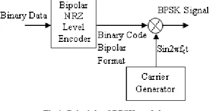
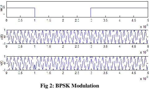
[image:1.595.315.537.607.721.2]For BPSK modulation technique based on phase modulation, BPSK modulation is realized with changed phase. For example, in fig 2, beginning of BPSK modulated signal’s period is positive values, if transmitting symbol is 1. But if transmitting signal is 0, beginning of BPSK modulated signal’s period is negative values. BPSK modulated signal is change at this cases.
Fig 1: Principle of BPSK modulator
Thereby, BPSK modulated signal is created. In Fig 2, it is shown that BPSK modulation. In this fig, m(t) is waveform of bipolar format, c(t) is carrier signal and s(t) is modulated signal.
Fig 2: BPSK Modulation
In BPSK, the transmitted signal is
s
(
t
)
m
(
t
)
c
(
t
)
scheme of BPSK modulation is as following [7] and fc is the frequencyof the carrier,
)
2
(
)
(
t
A
Sin
f
t
s
c
cif m(t)= logic 1
)
2
(
)
(
t
A
Sin
f
t
s
c
cif m(t)= logic 0 [image:2.595.54.295.123.266.2]
BPSK demodulator can be achieved from the BPSK waveform by using scheme of modulator in fig 3. The most important point for receiver, received signal is obtained quite correctly. As realizing in modulator input signal is firstly multiplied with a carrier of signal in demodulator. Next, multiplied signal is passed through integrator, then integrated signal is passed through a decision making device [7].
Fig 3: Principle of BPSK and BASK demodulator
2.2
BASK modulator and demodulator
BASK modulation technique is based on amplitude modulation. BASK modulation can be also considered for two cases: 0 and 1. If transmitting data is 1, BASK modulated signal is carrier signal. But when transmitting data is 0, BASK modulated signal is 0. In modulation, data bits are multiplied with a carrier signal and then modulated signal is created.
0
;
0
)
(
1
;
)
2
(
)
(
symbol
if
t
S
symbol
if
t
f
Sin
A
t
S
c
c(2)
Fig 4 is illustrated a principle BASK modulator.
Fig 4: Principle of BASK modulator
In fig 4, it is shown that principle of BASK modulator. Output of multiplier is modulated by binary code. This NRZ level encoder converts the input binary sequence to the signal suitable for product modulator [8]. In Fig 5, it is shown that BASK modulation.
Fig 5: BASK Modulation
In fig 3, it is shown that principle BASK demodulator.
3.
BPSK MODULATOR DESIGN OF
FPGA BASED
Using Quartus II complier, BPSK modulated signal can be created. Proposed block diagram in FPGA is shown in fig 6.
Fig 6: Principle of the BPSK system implemented on the FPGA
Using ADC, message signal is converted digital signal. Thereby, in FPGA, this signal can be processed and FPGA based BPSK modem can be created. Used bit separator separates one by one in 14 bits output of ADC. Bit separator was created using Very high speed integrated circuit Hardware Description Language.
[image:2.595.55.270.450.587.2] [image:2.595.315.538.521.647.2]If digital output of bit separator is 1, output of mux is carrier signal. However, digital output of bit separator is 0, output of mux is delayed carrier signal (180 degrees of phase delay). So, BPSK modulated signal was created. In Quartus II, created block of BPSK modulator is shown in fig 7.
Fig 7: In Quartus II created BPSK block
In fig 7, data_in, data_out, clk represent output of ADC, BPSK modulated signal, clock pulse respectively. Control block, rom, counter, bit separator and mux are embedded on one block (BPSK modulator block). Using control block, other blocks are controlled during operating time. If control block isn’t used, more blocks must be used. Because, for setting operating time, special time is only set using compare.
Fig 8:BPSK modulator in Quartus II
[image:3.595.318.541.186.324.2]In fig 8, Sinus datas was saved on sin_ph1 and sin_ph2. Sin_ph2 is 180 degrees of phase delay. Also, d_out is output of bit separator. Gate_of_mux acts as a selector. In fig 9, it is shown that the control block of BPSK modulator. In fig 9, it is shown that control block. Output of data counter is sending data numbers. Rom and bit_separator are enabling signals. These signals are connected to clk_en of relation blocks.
Fig 9: Control block ofBPSK modulator
4.
BASK MODULATOR DESIGN OF
FPGA BASED
[image:3.595.69.265.313.529.2]BASK based on FPGA application was implemented on Quartus II compiler. Also, both modulation and demodulation were implemented on FPGA. So, modem based on FPGA was created. Yet, in this paper BASK modulator was only represented using Quartus II complier. The principle of the BASK system implemented on the FPGA is illustrate in fig 10.
Fig 10:Principle of the BASK system implemented on the FPGA
[image:3.595.317.523.402.544.2]The output of created bit separator using Very high speed integrated circuit Hardware Description Language has one bit. According to output digital signal of bit separator (0, 1), mux selects one of two cases. Thereby BASK modulation was created on FPGA.
Fig 11:In Quartus II created BASK block
In fig 11, clk is clock pulse, data_in is output of ADC and data_out is BASK modulated signal. Also, this modulator contains two counters and roms, control block, bit separator and mux. In fig 13, it is shown that blocks of implemented BASK modulator in FPGA. According to output of bit separator, one of s1, s2 is selected by gate_of_mux. In fig 12, it is shown that created block of bit separator using VHDL.
[image:3.595.115.221.642.712.2] [image:3.595.371.483.652.737.2]Fig 13. BASK modulator in Quartus II
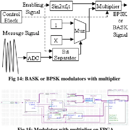
[image:4.595.347.509.258.406.2]In fig 14, it is shown that block scheme of BASK and BPSK modulator with multiplier FPGA-based. If multiplier is used in these modulators, transmitting time will rise. In fig 14, if X=0, modulator acts BASK while if X=-1, modulator acts BPSK. Fig 15 shows modulator with multiplier FPGA based.
Fig 14: BASK or BPSK modulators with multiplier
Fig 15: Modulator with multiplier on FPGA
5.
BASK AND BPSK BER
In an AWGN channel, the BER (Bit Error Rate) decreases approximately exponentially as the SNR (Signal to Noise Ratio) increases [9]. Straight BPSK produces good BER value at the receiver. Although the symbol error rate for BPSK is low that of BASK, BPSK transmits symbols at same the rate of BASK Bit error rate of BPSK can be shown at equation 4 while bit error rate of BASK cab be shown at equation 5.
0
2
N
E
Q
P
b b(4)
0
N
E
Q
P
b b(5)
In equation (4) or (5), Eb and No represent average energy per bit and noise power respectively. In fig 16, it is shown that plotting of BER performance of BPSK and BASK modulations using MATLAB. In fig 16, it is shown that BPSK has better performance than BASK resulting in the lowest BER for a given Eb/No. Yet, bit error rate comparison of BASK and BPSK modulation techniques aren’t alone criterion.
Fig 16: BER of BPSK and BASK modulation technique
6.
BPSK SIMULATION RESULT ON
FPGA
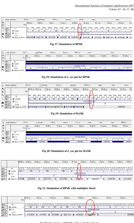
In fig 17, it is shown that simulation result of the BPSK modulation. In fig 17, d_in represent input of bit_separator and digital output of ADC. So Floating Point numbers is multiplied, BPSK signal (output of modulator) has hexadecimal format. This hexadecimal format is represented 32 bits. This numbers can be converted to decimal form using MATLAB. Because hexadecimal numbers are samples of BPSK signal, this numbers are converted to decimal form then plotting of BPSK signal can be created using plotting program. Figure in plotting program (BPSK modulated signal) is obtained (similar to fig 2). According to bit value of d_out (output of bit_separator), output of mux (phase of BPSK signal) are selected. Counter is number of transmitted samples. As shown fig 17, during transmit to one symbol, 500 samples are transmitted. Thanks to used control block, one symbol is transmitted bit per 500 samples.
7.
BASK SIMULATION RESULT ON
FPGA
[image:4.595.54.282.406.633.2]Fig 17: Simulation of BPSK
Fig 19: Simulation of BASK Fig 18: Simulation of d_out pin for BPSK
Fig 20: Simulation of d_out pin for BASK
[image:5.595.69.508.23.751.2]Fig 21: Simulation of BPSK with multiplier block
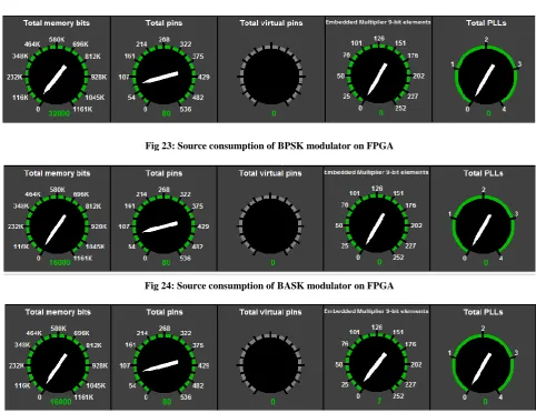
In FPGA kit, source consumption of BASK and BPSK modulation techniques can be also compared. BASK and BPSK modulators use ROM in FPGA hardware. Thereby these modulation techniques are using the memory. Because samples of carrier signal are saved ROM. According to saved bits number, used memory area on FPGA increases the same amount. In fig 23, fig 24, fig 25, it is shown that source consumption BASK and BPSK.
If fig 17 and fig 19 are viewed, it is shown that transmitting time of one bit is approximately 20 us. But in fig 21 and in fig 22, transmitting time of one bit is approximately 70 us. In fig 17 or 19, one sample is transmitted during two clock pulse. Each clock pulse has 50 MHz frequency. So, one period of clock pulse is 20 ns. Using sample number*period of clock pulse*number of clock pulse per sample, for 500 samples, transmitting time can be calculated. Result is 20us. But if fig 21 and fig 22 is viewed, more than 5 clock pulse was used for these simulations. If the simulation time is recalculated, simulation time results 70 us (7*500*20 ns=70 us).
If fig 23, fig 24 and fig 25 are viewed, it is illustrated that different source consumption for different modulation and different modulator algorithm. In fig 23 total memory bits are 32000. Because saved sample number in ROM is 500. Also, each sample is 32 bit (hexadecimal number) and used ROM number is two for phase1 and phase2. Thereby used memory source is 32000. For EP3C40F780C6 FPGA kit, used
frequency of clock pulse is only 50 MHz. So, PLL don’t use this paper. If PLL is used for this design, data rate is increased so clock frequency is rise. In addition to, total pin number is 80 (clk + counter + d_in + dout + Signal_of_BPSK = 1 + 32 + 14 + 1 + 32 = 80). Yet, pins of counter and d_out are used for information (sample number and changing symbol). Normally, used total pin number must 47. Also, a problem is 32 bits for BPSK. Because special digital to analog converter (DAC) must be used for convert to analog BPSK signal. But if floating point numbers are converted to lower bit format, special DAC isn’t required. Thereby used bit number is decreased.
Fig 24 shows source consumption of BASK modulation. BASK modulator is used one ROM. Thereby, BASK modulator use 16000 memory bits. Fig 25 shows source consumption BASK and BPSK modulator with multiplier. Used memory bits and embedded multiplier 9-bit elements are 16000 and 7 respectively.
8.
CONCLUSIONS
[image:6.595.59.542.71.443.2]Instead of fig 6 and fig 10, multiplier block was also used in this paper. But if multiplier block is used, modulation time will rise. Because operating time of multiplier block is least 5 clock pulses. Instead of multiplication, for each phase case (0 and 1), sample of different carrier signal was saved in ROM. Thereby, instead of 7 clock pulse, two clock pulses were used for each BPSK or BASK output sample. Fig 23: Source consumption of BPSK modulator on FPGA
Fig 24: Source consumption of BASK modulator on FPGA
[image:6.595.65.541.85.182.2]In addition, the purpose of this paper is can be implemented BPSK and BASK modulation techniques based on FPGA. Also, comparison to performance of implemented modulation techniques are analyzed It is shown that modulation techniques (BASK and BPSK) have disadvantage and advantage in simulation and plotting results. In this results, it is illustrated that BER of BASK high than BER of BPSK. Yet, bit transfer rate of BASK is as same as bit transfer rate of BPSK. Also, power consumption of BASK is low than BPSK. As shown in fig 23 and fig 24, source consumption for BASK modulation is less than BPSK modulation. In fig 25, it is shown that used ROM numbers less than in fig 23. But used multiplier is more than fig 23. In addition to, it is shown that changing of bit (0-1-0) is realized on each 500 sample. In BASK modulator, for 0 bit, it is shown that sending data is 0 while for 1 bit, it is shown that sending data is samples of carrier signal. In BPSK modulator, for 0 bit, it is illustrated that processing data is samples of delayed carrier signal (180 degrees of phase delay), for 1 symbol, it is illustrated that processing data is samples of carrier signal.
9.
REFERENCES
[1] Park, H., C., “Power and bandwidth efficient constant-envelope BPSK signals and its continuous phase modulation”, IEE Proceedings Communications, vol. 152, No. 3, June 2005
[2] Jae, C., M., Eon, J., S., “Design of Low Power ASK CMOS Demodulator Circuit for RFID Tag”, 2010 IEEE International Conference of Electron Devices and Solid-State Circuits (EDSSC), pp. 1-4, 2010..
[3] Sanni, A., Vilches, A., Toumazou, C.,” Inductive and Ultrasonic Multi-Tier Interface for Low-Power, Deeply Implantable Medical Devices”, Transactions on Biomedical Circuits and Systems, vol. PP, pp. 1-12, 2012
[4] Diao, S., Zheng, Y., Gao, Y., Cheng, S., J., Yuan, X., Je,
M., Heng, C.,” A 50-Mb/s CMOS QPSK/O-QPSK
Transmitter Employing Injection Locking for Direct Modulation”, Microwave Theory and Techniques, IEEE Transactions on, vol. 60, pp. 120-130, 2012.
[5] Byun, G.,S., Kim, Y., Kim, J., Tam, W.-S., Chang, F., “An Energy-Efficient and High-Speed Mobile Memory I/O Interface Using Simultaneous Bi-Directional Dual (Base+RF)-Band Signaling”, IEEE Journal Of Solıd-State Cırcuıts, Vol. 47, No. 1, January 2012
[6] Lane, P., M., Kitayama, K., “The interaction between fibre dispersion and laser phase noise in an ASK self-heterodyne millimetre-wave fibre-radio system”, IEE Proceedings Optoelectronics, vol. 146, no. 4, August 1999
[7] Das, A., “Digital Communication: Principles and System Modelling ”, Springer-Verlag Berlin Heidelberg, 2010 [8] J. S. Chitode, “Analog And Digital Communication”,
Technical Publications Pune, India, 2009.
[9] Molisch, A., F., “Wireless Communication”, john Wiley
& Sons, UK,2011.