N A N O E X P R E S S
Open Access
Impact of electrically formed interfacial layer and
improved memory characteristics of IrO
x
/high-
κ
x
/
W structures containing AlO
x
, GdO
x
, HfO
x
, and
TaO
x
switching materials
Amit Prakash
1, Siddheswar Maikap
1,2*, Writam Banerjee
1, Debanjan Jana
1and Chao-Sung Lai
2Abstract
Improved switching characteristics were obtained from high-κoxides AlOx, GdOx, HfOx, and TaOxin IrOx/high-κx/W structures because of a layer that formed at the IrOx/high-κxinterface under external positive bias. The surface roughness and morphology of the bottom electrode in these devices were observed by atomic force microscopy. Device size was investigated using high-resolution transmission electron microscopy. More than 100 repeatable consecutive switching cycles were observed for positive-formatted memory devices compared with that of the negative-formatted devices (only five unstable cycles) because it contained an electrically formed interfacial layer that controlled‘SET/RESET’current overshoot. This phenomenon was independent of the switching material in the device. The electrically formed oxygen-rich interfacial layer at the IrOx/high-κxinterface improved switching in both via-hole and cross-point structures. The switching mechanism was attributed to filamentary conduction and oxygen ion migration. Using the positive-formatted design approach, cross-point memory in an IrOx/AlOx/W structure was fabricated. This cross-point memory exhibited forming-free, uniform switching for >1,000 consecutive dc cycles with a small voltage/current operation of ±2 V/200μA and high yield of >95% switchable with a large resistance ratio of >100. These properties make this cross-point memory particularly promising for high-density applications. Furthermore, this memory device also showed multilevel capability with a switching current as low as 10μA and a RESET current of 137μA, good pulse read endurance of each level (>105cycles), and data retention of >104s at a low current compliance of 50μA at 85°C. Our improvement of the switching characteristics of this resistive memory device will aid in the design of memory stacks for practical applications.
Keywords:Resistive switching; W/TaOx; Ti nanolayer; Oxygen ion migration; Nanofilament
Background
Resistive random access memory (RRAM) with a simple metal-insulator-metal structure shows promising charac-teristics in terms of scalability, low power operation, and multilevel data storage capability and is suitable for next-generation memory applications [1-4]. RRAM de-vices with simple structure and easy fabrication process that are compatible with high-density 3D integration [5] will be needed in the future. Various oxide switching
materials such as HfOx [6-9], TaOx [3,10-15], AlOx [16-19], GdOx [20], TiOx [21-23], NiOx [24,25], ZrOx [26-29], ZnO [30-32], SiOx[33], and GeOx[34-36] have been used in nanoscale RRAM applications. However, their nonuniform switching and poorly understood switching mechanisms are currently the bottlenecks for the design of nanoscale resistive switching memory. Gen-erally, inert metal electrodes [4] and various interfacial methods are used to improve resistive switching memory characteristics. We previously reported polarity-dependent improved memory characteristics using IrOx nanodots (NDs) in an IrOx/AlOx/IrOx-NDs/AlOx/W structure [16]. However, improved memory performance using different high-κ oxide switching materials such as AlOx, GdOx,
* Correspondence:[email protected]
1Thin Film Nano Technology Laboratory, Department of Electronic
Engineering, Chang Gung University, Tao-Yuan 333, Taiwan
2Biomedical Engineering Research Center, Department of Electronic
Engineering, Chang Gung University, Tao-Yuan 333, Taiwan
HfOx, and TaOx in IrOx/high-κx/W structures has not been reported yet. Using different high-κ oxides in the same structure may reveal a unique way to design novel RRAM devices for practical applications. Electrical forma-tion of an interfacial layer at the IrOx/high-κx interface is important to improve resistive switching memory charac-teristics. Using this approach, high-density memory could be achieved using an IrOx/AlOx/W cross-point structure, which we also report here.
In this study, we show that the electrically formed oxygen-rich interfacial layer at the IrOx/high-κx inter-face in an IrOx/high-κx/W structure plays an import-ant role in improving the resistive switching memory characteristics of the structure. The positive-formatted (PF) devices exhibited more switching cycles com-pared to the negative-formatted (NF) ones and do not depend on the switching material. When the pristine resistive memory device is formed using positive po-larity bias on the TE, it is termed as PF, while the negative voltage-formed device is termed as an NF device. PF devices with similar switching behavior are obtained using different high-κ oxide films of AlOx, GdOx, HfOx, and TaOx. The switching mechanism is the formation/oxidation of oxygen vacancies in a conducting filament by controlling the migration of oxygen ions through the electrically formed interfacial layer. This unique phenomenon helps to design high-density cross-point memory using an IrOx/AlOx/W structure. This cross-point memory was forming-free, exhibiting 1,000 consecutive ‘dc’ cycles at a current compliance (CC) of <200 μA and a small operation voltage of ±2 V, highly uniform switching (yield >95%) with multilevel capability (at least four different levels of low resistance state (LRS)). The device can be switched
even using a very small current of 10μA, which makes it useful for low power applications. The surface morphology and roughness of the structure were observed by atomic force microscopy (AFM). The device size and interfaces of layers were investigated by transmission electron micros-copy (TEM). These observations show that the improved performance of this device structure can be attributed to the electrically formed O-rich interfacial layer at the top electrode/filament interface. The devices have also shown good read endurance of >105cycles and data retention at 85°C under a low CC of 50μA.
Methods
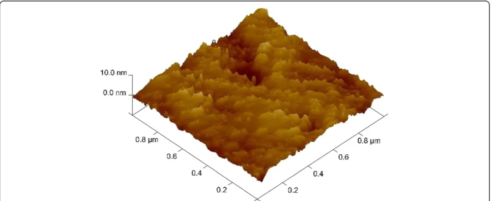
[image:2.595.57.542.514.712.2]Resistive switching memory devices using high-κ ox-ides AlOx, GdOx, HfOx, and TaOx in a standard via-hole IrOx/high-κx/W structure (Device: S1) were fabricated. A W layer with a thickness of approxi-mately 100 nm as a bottom electrode (BE) was de-posited on SiO2 (200 nm)/Si substrates. Figure 1 shows an AFM image taken in tapping mode using an Innova Scanning Probe Microscope system (Bruker, Madison, WI, USA) of a deposited W film surface. The average and root mean square (RMS) roughness of the surface were 0.91 and 1.18 nm, respectively. An SiO2layer with a thickness of approximately 150 nm was then depos-ited at low temperature on each W BE. Photolithography and dry etching techniques were used to form holes of dif-ferent sizes in the range of 0.4 to 8 μm in the structure. Then, AlOxand HfOxfilms were deposited by sputtering, and GdOx and TaOx films were deposited by electron beam evaporation. The thickness of each high-κ film was 10 to 15 nm. The top electrode (TE) of IrOx (approxi-mately 200 nm thick) was deposited by reactive sputtering using a pure Ir target and O2 as the reactive gas. The
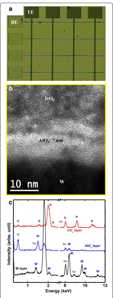
final devices with a structure of IrOx/high-κx/W were obtained after a lift-off process. The structure of the memory devices and thicknesses of all deposited layers were observed by TEM at an energy of 200 keV. Figure 2a shows a typical cross-sectional TEM image of an IrOx/TaOx/W resistive memory stack with a via-hole structure (S1). The typical device size was 2 × 2 μm. The high-resolution transmission electron microscopy (HRTEM) image taken inside the via-hole (Figure 2c) reveals the formation of two layers; one is TaOx and the other one is WOx, which is formed by the surface oxidation of the W BE because of the ex situ fabrica-tion process. To confirm the thickness of the depos-ited TaOx layer, a HRTEM image was acquired from the area outside the via-hole, i.e., on the SiO2 (Figure 2b). The amorphous TaOx layer was approxi-mately 9nm thick, confirming that the thickness of the polycrystalline WOx layer inside the via-hole was ap-proximately 5 nm (Figure 2c). This kind of bilayer
structure (high-κ/WOx) was observed in all of the fab-ricated resistive memory stacks investigated (TEM im-ages not shown here).
[image:3.595.57.539.346.697.2]To obtain high-density memory, W films with a thickness approximately 100 nm were deposited on the SiO2 (200 nm)/Si substrates by sputtering to form IrOx/AlOx/W cross-point structures (Device: S2), which were patterned using photolithography and wet etching techniques to form W BE stripes. Cross-point memory with different sizes ranging from 4 × 4 to -50 × -50 μm was fabricated by another lithography step to pattern the TE stripes using a lift-off method. To obtain forming-free cross-point memory, the thickness of the AlOx layer was 7 nm. Figure 3a shows a typical optical microscope (OM) image of a fabricated resistive memory device with an IrOx/ AlOx/W cross-point structure (Device: S2) with a size of 4 × 4 μm. The AlOx layer sandwiched between the IrOx TE and W BE is clearly seen in a cross-sectional
Figure 2TEM and HRTEM images of IrOx/TaOx/W stack with via-hole structure and size of 2 × 2μm. (a)TEM image.(b)HRTEM image
outside of active region. The TaOxfilm is approximately 9 nm thick and amorphous.(c)HRTEM image in the active region. A WOxlayer with a
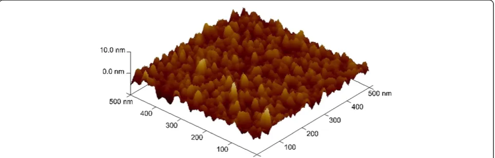
HRTEM image of this device (Figure 3b). The surface of the W BE is rough. The energy-dispersive X-ray spectra shown in Figure 3c confirm that the re-spective layers contain Ir, Al, O, and W. To further examine the roughness and surface morphology of the W BE, an AFM image of the W BE surface was obtained, as shown Figure 4. The average and RMS surface roughness of the W BE were 1.05 and 1.35 nm, respectively, which are higher than those of the W BE in the devices with via-hole structures (S1, as shown in Figure 1). This morphological difference is also found to be important to improve the resistive switching behavior of cross-point memory devices, which will be discussed later. However, we first designed the via-hole PF devices (S1) and then the cross-point structure (S2) to improve memory charac-teristics. A bias was applied to the TE, and the BE was electrically grounded in both of the structures.
Results and discussion
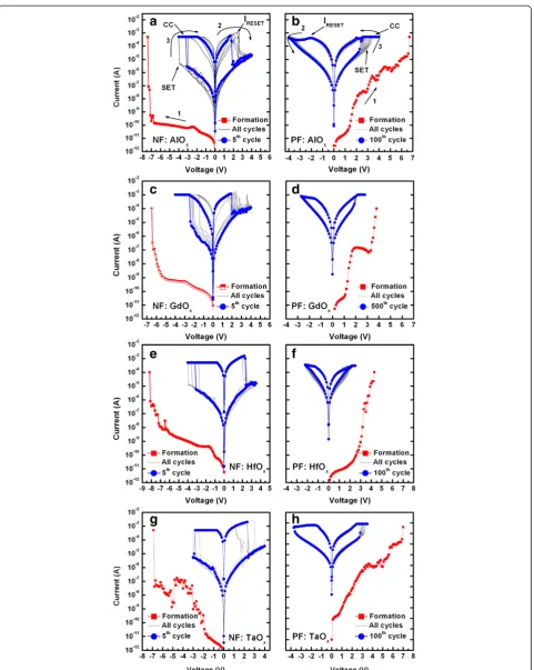
[image:4.595.56.291.84.702.2]The current–voltage (I-V) properties of the NF and PF devices (S1) with bipolar resistive switching mem-ory characteristics are shown in Figure 5. The sweep-ing voltage is shown by arrows 1 to 3. Figure 5a shows the typical I-V curves of the NF devices with an IrOx/AlOx/W structure. A high formation voltage of about <−7.0 V was required with very low leakage current. After formation, the first five consecutive switching cycles show large variations in low and high resistance states as well as SET/RESET voltages with higher maximum reset current (IRESET) than the set or CC. Similar behavior can be observed for all of the other resistive memory devices containing GdOx, HfOx, and TaOx as switching materials (Figure 5c,e,g). Figure 5b shows typical consecutive I-V switching curves for 100 cycles together with the formation curve at a positive voltage obtained for the AlOx -based device with a via-hole structure. Remarkable improvement in the consecutive switching cycles with a tight distribution of LRS and high resistance state (HRS) and SET/RESET voltage was obtained, which is suitable for RRAM devices. Furthermore, IRESET is not higher than that of the CC unlike the NF devices, which indicates that the PF devices are mainly elec-tric field-dominated, and switching occurs near the interface. In contrast, electric field-induced thermal effects are also important in the case of the NF de-vices, and large variations in switching occur. The uncontrolled current flow through the filament in the
Figure 3Morphology and composition of an IrOx/AlOx/W
cross-point structure. (a)OM image.(b)Cross-sectional TEM image of the cross-point memory device. The thickness of AlOxfilm is
NF device will enhance Joule heating as well as the abrupt breaking of the filament, and the RESET current curve is suddenly reduced. On the other hand, the RESET current in the PF device is changed slowly because of the series resistance which will con-trol the current flow through the filament precisely. That is why the current changes slowly in the PF de-vices. It is interesting to note that the resistance of LRS of PF device is higher (approximately 10 kΩ) than that of the NF device (approximately 1 kΩ), and the controlling current through the series resistance of the PF devices will have also lower HRS than that of the NF devices. Therefore, the NF devices will have lower value of LRS and higher value of HRS, which results in the higher resistance ratio as com-pared to the PF devices. All of the other fabricated PF devices show a similar improvement in switching, as shown in Figure 5d,f,h. The leakage current is smaller in the negative-voltage region (Figure 5a) than in the positive-voltage region (Figure 5b) because of the higher barrier height for electron injection im-posed by the higher work function of the IrOx TE (ΦIrO2> 5 eV [37] and ΦW of approximately 4.55 eV [38]) when a negative voltage is applied. It is import-ant to note that all of the resistive memory devices show similar switching characteristics irrespective of the switching material. This suggests that in the elec-trode materials, their reactivity and top/bottom selec-tion are very important for RRAM stacks, which allow their switching properties as well as device per-formance to be improved by controlling SET/RESET polarity. Therefore, this unique study using the switching materials AlOx, GdOx, HfOx, and TaOx in an IrOx/high-κx/W structure provides clues for im-proving the design of nanoscale high-performance nonvolatile memory.
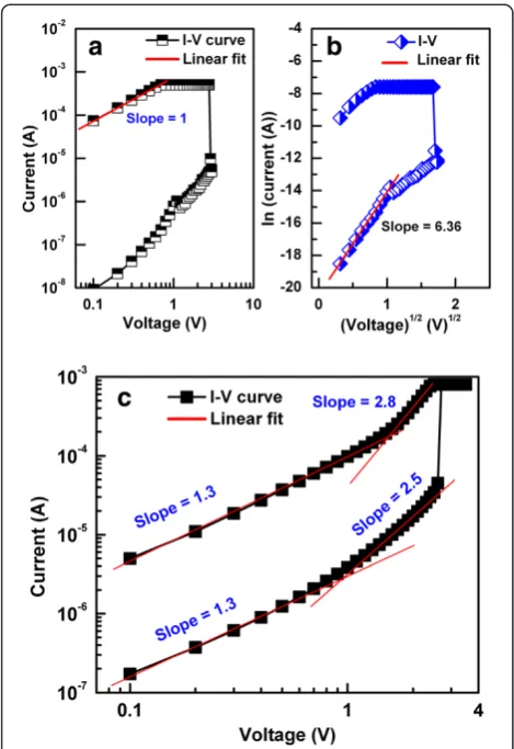
[image:5.595.58.540.90.244.2]To determine the current conduction mechanism in the devices, the I-Vcurves of the HRS and LRS of the NF (Figure 6a,b) and PF (Figure 6c) devices with an IrOx/TaOx/W structure were replotted and fitted linearly. For the NF devices, the LRS was fitted to ohmic conduction with a slope of approximately 1, whereas HRS was consistent with the Schottky emission model. Both LRS and HRS were consistent with a trap-controlled (TC) space charge-limited conduction (SCLC) mechanism following ohmic conduction in the low-voltage region and square law in the high-low-voltage region for the PF devices. When the positive/negative sweep voltage increases in a pristine device, the metal (M)-O bonds in high-κ oxides AlOx, GdOx, HfOx, and TaOx break and the generated oxygen ions (O2−) will drift to-wards TE or BE according to the direction of the applied field. When a sufficient number of O2−ions are gener-ated, the current suddenly increases because of the for-mation of a conducting filament and the device enters the SET state. In PF devices, the migrated O2−form an O-rich layer that is comparatively insulating (i.e., an electrically formed interfacial layer) at the TE/high-κ interface because of the inert nature of the IrOx elec-trode (which even rejects oxygen) under SET operation (Figure 7a). This interface acts as a series resistance and helps to reduce the overshoot current (Figure 8) as well as increasing the LRS (10 kΩfor PF devices vs. 1 kΩfor NF devices). This is why the PF devices show improved switching properties compared with the NF ones. Under RESET operation of a PF device, O2−will be repelled away from the TE and oxidize the oxygen vacancies in the filament, converting the device into a HRS (Figure 7b). Conversely, when O2−ions migrate towards the BE in the case of NF devices, they will react with the semi-reactive, partially oxidized W BE to form WOx, which can serve as an oxygen reservoir without
Figure 5Current–voltage (I-V) switching characteristics of devices with via-hole structure under negative (NF) and positive formation (PF). (a, c, e, and g)Switching curves of NF devices containing AlOx, GdOx, HfOx, and TaOxswitching materials, respectively, in an IrOx/high-κx/W
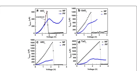
changing its conductivity. This results in the formation of multiple oxygen filaments (Figure 7c). Under RESET operation of the NF devices, both Joule heating and O2− migration from the W BE/high-κx interface will lead to the oxidation of the conducting filament (Figure 7d). Overshoot RESET current is also observed (Figure 8). The maximum IRESET of the devices containing AlOx, GdOx, HfOx, and TaOx switching materials were 616, 1,180, 1,628, and 2,741 μA, respectively, for NF devices, and 409, 543, 276, and 684 μA, respectively, for the PF devices (Figure 8a,b,c,d). The RESET current of NF de-vices is higher in all cases than the PF dede-vices prob-ably because of higher current overshoot in the NF devices. Current overshoot degrades the switching material because uncontrolled oxygen vacancy fila-ments form. For the NF devices, the multifilafila-ments can be formed due to oxygen ion migration [39]; however, the filaments are ruptured by thermal effect
under RESET operation, i.e., the thermal dissolution of oxygen vacancy filaments may result the uncon-trolled filaments to break as well as the SET oper-ation will not be controlled in consequence. The thermal dissolution of conducting filaments under RESET operation on NiOx-based resistive switching memories was also reported by Ielmini et al. [25] and Long et al. [40,41]. In contrast, the damage is negli-gible in the PF devices because of the presence of an electrically formed interfacial layer at the TE/high-κ interface. The filament diameter is readily controlled in the PF devices because of the electrically formed interface. This kind of asymmetric resistive memory stack will help to optimize resistive switching and de-vice performance.
[image:7.595.56.291.88.430.2]High-density memory devices are required for future applications. Resistive memory devices with cross-point architecture show promise to achieve high-density memory. Therefore, we fabricated the re-sistive memory stacks of IrOx/high-κx/W with cross-point structure (S2). Figure 9 shows the typical I-V curves of 1,000 consecutive dc switching cycles obtained for an IrOx/AlOx/W stack. The applied volt-age sweep direction is indicated by arrows marked 1 to 4. It is interesting to note that no formation process was required to obtain switching, which is very useful for practical realization of RRAM. Excel-lent bipolar resistive switching is obtained with a small SET/RESET voltage of approximately ±1.2 V. Furthermore, these results show that a rough surface with nano tips (Figure 4) enhances the electric field on the tips and makes it easier to control the switching cycles. To enhance the resistive switching memory performance, the Cu nanocrystals (NCs) in an Ag/ZrO2/Cu-NC/Pt structure was also reported by Liu et al. [42,43]. They mentioned that the electric field could be enhanced and controlled through Cu NC and hence improve the switching characteristics. In our device, a large resistance ratio of >100 with a small operation voltage of ±2 V and CC of 200 μA were obtained for the IrOx/AlOx/W stack. IRESET in-creased from 98 to 130 μA from 1 to 1,000 cycles, which indicates stronger filament formation after a few switching cycles. A similar increase in RESET current with switching cycle was also reported for a Cu/Ti/TaOx/W structure [10]. All cross-point mem-ory devices showed excellent switching with high yields of >95%, which is suitable for nonvolatile mem-ory applications. Both the LRS and HRS were stable during the 1,000 cycles with a narrow distribution of SET/RESET voltages and ratio of LRS to HRS. The underlying switching mechanism was the formation/ oxidation of oxygen-vacancy filaments, which was controlled by the electrically formed oxygen-rich layer
Figure 6FittedI-Vcharacteristics of PF and NF devices with IrOx/TaOx/W structure. (a)LRS of NF devices fitted ohmic behavior.
Figure 7Resistive switching mechanism of the PF and NF devices.PF and NF devices under(a, c)SET and(b, d)RESET operations.
Figure 8RESET phenomena for the PF and NF devices.RESET currents of NF and PF devices containing(a)AlOx,(b)GdOx,(c)HfOx, and(d)
[image:8.595.58.539.455.706.2]formed at the TE/AlOx interface under an external field, as for the via-hole devices (S1). The memory devices can be used for multilevel data storage even under harsh conditions (85°C). Figure 10a shows an image of our auto measurement program screen during multilevel capability testing of a device. Linear I-Vcurves at five different levels of LRS are obtained by controlling the CCs from 10 to 200 μA. The cor-responding resistances of the LRS read at +0.2 V are approximately 800, 300, 70, 30, and 12 kΩ for CC of 10, 30, 50, 100, and 200 μA, respectively (Figure 10b). Even though this resistive memory device is switch-able at a low CC of 10 μA, its IRESET is higher, ap-proximately 137 μA (Figure 10c). Figure 10d shows the dc endurance of the multilevel memory of the same device. The HRS remains almost unchanged when CC is varied from 10 to 200 μA. Each LRS level can be switched uniformly for >100 cycles. Fur-thermore, pulse read endurance and retention tests of the multilevel of memory device were also performed, as shown in Figure 11a,b, respectively. Each level of
Figure 9One thousand consecutive dc switching cycles of IrOx/
AlOx/W cross-point memory.The switching was obtained at a CC
of 200μA and a low operation voltage of ±2 V for the PF device with a size of 4 × 4μm.
[image:9.595.56.541.360.682.2]LRS and HRS were successfully read for more than 105 cycles at a read voltage of 0.2 V without any dis-turbance for CC of 50 to 200 μA (Figure 11a). The multilevel LRSs are nonvolatile because the retention test shows good stability of these resistance states
for >104 s for CC from 50 to 200 μA at room temperature (Figure 11b). Good data retention of >104s for a CC of 50 μA at 85°C is also observed. The program/erase endurance of approximately 1,000 cycles of the memory device at a current of 200 μA is also shown in Figure 11c. Notwithstanding, we have used a program/erase pulse of 500 μs due to our system limitation. However, the high switching speed (<0.3 ns) of RRAM in HfOx and TaOx-based devices were reported by other research groups [44,45]. The robust electrical performance of these es-sential memory properties makes this device very promising for future high-density nanoscale nonvola-tile memory applications.
Conclusions
Improved resistive switching characteristics independent of switching material are observed for IrOx/high-κx/W stacks with a via-hole structure fabricated by positive formation because they contain an electrically formed interfacial layer. High-κ oxides AlOx, GdOx, HfOx, and TaOx were used as switching materials, and similar switching behavior with improved switching uniformity was obtained because overshoot current was minimized in the via-hole structure. AFM images revealed that the BEs of cross-point devices had a higher surface rough-ness than that of the via-hole devices, which facilitated forming-free switching, improving the switching charac-teristics. Excellent resistive switching was obtained in Ir/ AlOx/W cross-point structures using the same PF via-hole design. These devices showed forming-free resistive switching with excellent switching uniformity (>95% yield) over 1,000 dc cycles (approximately 1,000 ac cycles) under low operation voltage/current of ±2 V/200 μA. Multilevel LRSs were obtained by controlling the CCs from 10 to 200μA with a pulse read endurance of >105cycles for each level and data retention at room temperature and 85°C under a low CC of 50 μA. This study reveals a route to design nanoscale nonvolatile memory with improved characteristics.
Competing interests
The authors declare that they have no competing interests.
Authors’contributions
AP fabricated and analyzed both the TaOxand HfOxmemories and
developed the auto measurement program. WB fabricated the AlOx-based
memory. DJ fabricated the GdOx-based memory. This research work was
carried out under the instruction of SM. CSL offered the fabrication process. All of the authors revised the manuscript. All authors read and approved the final manuscript.
Acknowledgements
[image:10.595.57.291.88.605.2]This work was supported by the National Science Council (NSC), Taiwan, under contract number: NSC-101-2221-E-182-061. The authors thank Electronic and Optoelectronic Research Laboratories, Industrial Technology Research Institute, Hsinchu, Taiwan, for their partially experimental support.
Figure 11Stability and data retention of a cross-point device. (a)Long read pulse endurance of >105cycles and(b)data retention
of >104s are observed with CCs of 50, 100, and 200μA. Good data
Received: 9 July 2013 Accepted: 15 August 2013 Published: 6 September 2013
References
1. Waser R, Dittmann R, Staikov G, Szot K:Redox-based resistive switching memories-nanoionic mechanisms, prospects, and challenges.Adv Mater
2009,21:2632.
2. Sawa A:Resistive switching in transition metal oxides.Mater Today2008,
11:28.
3. Lee MJ, Lee CB, Lee D, Lee SR, Chang M, Hur JH, Kim YB, Kim CJ, Seo DH, Seo S, Chung UI, Yoo IK, Kim K:A fast, high-endurance and scalable non-volatile memory device made from asymmetric Ta2O(5-x)/TaO(2-x)bilayer structures.Nat Mater2011,10:625.
4. Liu Q, Sun J, Lv H, Long S, Yin K, Wan N, Li Y, Sun L, Liu M:Real-time observation on dynamic growth/dissolution of conductive filaments in oxide-electrolyte-based ReRAM.Adv Mater1844,2012:24.
5. Yu S, Chen HY, Gao B, Kang J, Wong HSP:HfOx-based vertical resistive switching random access memory suitable for bit-cost-effective three-dimensional cross-point architecture.ACS Nano2013,
7:2320.
6. Lee HY, Chen PS, Liu WH, Wang SM, Gu PY, Hsu YY, Tsai CH, Chen WS, Chen F, Tsai MJ, Lien C:Robust high-resistance state and improved endurance of HfOxresistive memory by suppression of current overshoot.
IEEE Electron Device Lett2011,32:1585.
7. Yu S, Guan X, Wong HSP:Conduction mechanism of TiN/HfOx/Pt resistive switching memory: a trap-assisted-tunneling model.Appl Phys Lett2011,
99:063507.
8. Chen YY, Goux L, Clima S, Govoreanu B, Degraeve R, Kar GS, Fantini A, Groeseneken G, Wouters DJ, Jurczak M:Endurance/retention trade-off on HfO2/metal cap1T1R bipolar RRAM.IEEE Trans Electron Dev2013,
60:1114.
9. Lee J, Bourim EM, Lee W, Park J, Jo M, Jung S, Shin J, Hwang H:
Effect of ZrOx/HfOxbilayer structure on switching uniformity and reliability in nonvolatile memory applications.Appl Phys Lett2010,
97:172105.
10. Rahaman SZ, Maikap S, Tien TC, Lee HY, Chen WS, Chen F, Kao MJ, Tsai MJ:
Excellent resistive memory characteristics and switching mechanism using a Ti nanolayer at the Cu/TaOxinterface.Nanoscale Res Lett2012, 7:345.
11. Prakash A, Maikap S, Lai CS, Lee HY, Chen WS, Chen F, Kao MJ, Tsai MJ:
Improvement uniformity of resistive switching parameters by selecting the electroformation polarity in IrOx/TaOx/WOx/W structure.Jpn J Appl
Phys2012,51:04DD06.
12. Chen C, Song C, Yang J, Zeng F, Pan F:Oxygen migration induced resistive switching effect and its thermal stability in W/TaOx/Pt structure. Appl Phys Lett2012,100:253509.
13. Prakash A, Maikap S, Chiu HC, Tien TCS, Lai CS:Enhanced resistive switching memory characteristics and mechanism using a Ti nanolayer at the W/TaOxinterface.Nanoscale Res Lett2013,8:288.
14. Ninomiya T, Wei Z, Muraoka S, Yasuhara R, Katayama K, Takagi T:
Conductive filament scaling of TaOxbipolar ReRAM for improving data retention under low operation current.IEEE Trans Electron Dev2013,
60:1384.
15. Yang JJ, Zhang MX, Strachan JP, Miao F, Pickett MD, Kelley RD, Medeiros-Ribeiro G, Williams RS:High switching endurance in TaOxmemristive devices.Appl Phys Lett2010,97:232102.
16. Banerjee W, Maikap S, Lai CS, Chen YY, Tien TC, Lee HY, Chen WS, Chen FT, Kao MJ, Tsai MJ, Yang JR:Formation polarity dependent improved resistive switching memory characteristics using nanoscale (1.3 nm) core-shell IrOxnano-dots.Nanoscale Res Lett 2012,7:194.
17. Banerjee W, Maikap S, Rahaman SZ, Prakash A, Tien TC, Li WC, Yang JR:Improved resistive switching memory characteristics using core-shell IrOxnano-dots in Al2O3/WOxbilayer structure.J Electrochem Soc2012,159:H177.
18. Wu Y, Yu S, Lee B, Wong P:Low-power TiN/Al2O3/Pt resistive switching device with sub-20μA switching current and gradual resistance modulation.J Appl Phys2011,110:094104.
19. Fang RC, Sun QQ, Zhou P, Yang W, Wang PF, Zhang DW: High-performance bilayer flexible resistive random access memory based on low-temperature thermal atomic layer deposition.Nanoscale Res Lett
2013,8:92.
20. Jana D, Maikap S, Tien TC, Lee HY, Chen WS, Chen FT, Kao MJ, Tsai MJ:
Formation-polarity-dependent improved resistive switching memory performance using IrOx/GdOx/WOx/W structure.Jpn J Appl Phys2012, 51:04DD17.
21. Yang L, Kuegeler C, Szot K, Ruediger A, Waser R:The influence of copper top electrodes on the resistive switching effect in TiO2thin films studied by conductive atomic force microscopy.Appl Phys Lett
2009,95:013109.
22. Yang JJ, Pickett MD, Li X, Ohlberg DAA, Stewart DR, Williams RS:
Memristive switching mechanism for metal/oxide/metal nanodevices. Nat Nanotechnol2008,3:429.
23. Park J, Biju KP, Jung S, Lee W, Lee J, Kim S, Park S, Shin J, Hwang H:Multibit operation of TiOx-based ReRAM by Schottky barrier height engineering.
IEEE Electron Dev Lett2011,32:476.
24. Lee SR, Char K, Kim DC, Jung R, Seo S, Li XS, Park GS, Yoo IK:Resistive memory switching in epitaxially grown NiO.Appl Phys Lett2007,91:202115. 25. Ielmini D, Nardi F, Cagli C:Physical models of size-dependent
nanofilament formation and rupture in NiO resistive switching memories.Nanotechnology2011,22:254022.
26. Guan W, Long S, Jia R, Liu M:Nonvolatile resistive switching memory utilizing gold nanocrystals embedded in zirconium oxide.Appl Phys Lett
2007,91:062111.
27. Wang SY, Lee DY, Tseng TY, Lin CY:Effects of Ti top electrode thickness on the resistive switching behaviors of rf-sputtered ZrO2memory films.
Appl Phys Lett2009,95:112904.
28. Li Y, Long S, Lv H, Liu Q, Wang Y, Zhang S, Lian W, Wang M, Zhang K, Xie H, Liu S, Liu M:Improvement of resistive switching characteristics in ZrO2film by embedding a thin TiOxlayer.Nanotechnology2011,22:254028.
29. Lin CC, Chang YP, Lin HB, Lin CH:Effect of non-lattice oxygen on ZrO2 -based resistive switching memory.Nanoscale Res Lett2012,7:187. 30. Chiu FC, Li PW, Chang WY:Reliability characteristics and conduction
mechanisms in resistive switching memory devices using ZnO thin films. Nanoscale Res Lett2012,7:178.
31. Peng CN, Wang CW, Chan TC, Chang WY, Wang YC, Tsai HW, Wu WW, Chen LJ, Chueh YL:Resistive switching of Au/ZnO/Au resistive memory: an in situ observation of conductive bridge formation.Nanoscale Res Lett2012,
7:559.
32. Younis A, Chu D, Li S:Bi-stable resistive switching characteristics inTi-doped ZnO thin films.Nanoscale Res Lett2013,8:154.
33. Liu CY, Huang JJ, Lai CH, Lin CH:Influence of embedding Cu nano-particles into a Cu/SiO2/Pt structure on its resistive switching.Nanoscale
Res Lett2013,8:156.
34. Rahaman SZ, Maikap S, Chen WS, Lee HY, Chen FT, Kao MJ, Tsai MJ:
Repeatable unipolar/bipolar resistive memory characteristics and switching mechanism using a Cu nanofilament in a GeOxfilm.Appl Phys
Lett2012,101:073106.
35. Cheng CH, Chin A, Yeh FS:Ultralow switching energy Ni/GeOx/HfON/TaN RRAM.IEEE Electron Dev Lett2011,32:366.
36. Prakash A, Maikap S, Rahaman SZ, Majumdar S, Manna S, Ray SK:Resistive switching memory characteristics of Ge/GeOxnanowires and evidence of oxygen ion migration.Nanoscale Res Lett2013,8:220.
37. Banerjee W, Maikap S, Tien TC, Li WC, Yang JR:Impact of metal nano layer thickness on tunneling oxide and memory performance of core-shell iridium-oxide nanocrystals.J Appl Phys2011,110:074309.
38. Michaelson HB:The work function of the elements and its periodicity. J Appl Phys1977,48:4729.
39. Prakash A, Maikap S, Lai CS, Tien TC, Chen WS, Lee HY, Chen FT, Kao MJ, Tsai MJ:Bipolar resistive switching memory using bilayer TaOx/WOxfilms.
Solid-State Electron2012,77:35.
40. Long S, Cagli C, Ielmini D, Liu M, Sune J:Analysis and modeling of resistive switching statistics.J Appl Phys2012,111:074508. 41. Long S, Cagli C, Ielmini D, Liu M, Suñé J:Reset statistics of NiO-based
resistive switching memories.IEEE Electron Dev Lett2011,32:1570. 42. Liu Q, Long S, Wang W, Tanachutiwat S, Li Y, Wang Q, Zhang M, Huo Z,
Chen J, Liu M:Low-power and highly uniform switching in ZrO2-Based ReRAM with a Cu nanocrystal insertion layer.IEEE Electron Dev Lett2010,
31:1299.
44. Lee HY, Chen YS, Chen PS, Gu PY, Hsu YY, Wang SM, Liu WH, Tsai CH, Sheu SS, Chiang PC, Lin WP, Lin CH, Chen WS, Chen FT, Lien CH, Tsai MJ:
Evidence and solution of over-RESET problem for HfOxbased resistive memory with sub-ns switching speed and high endurance.Tech Dig - Int Electron Dev Meet2010:19. 7.1.
45. Torrezan AC, Strachan JP, Medeiros-Ribeiro G, Williams RS:Sub-nanosecond switching of a tantalum oxide memristor.Nanotechnology2011,
22:485203.
doi:10.1186/1556-276X-8-379
Cite this article as:Prakashet al.:Impact of electrically formed interfacial layer and improved memory characteristics of IrOx/high-κx/W structures
containing AlOx, GdOx, HfOx, and TaOxswitching materials.Nanoscale
Research Letters20138:379.
Submit your manuscript to a
journal and benefi t from:
7 Convenient online submission 7 Rigorous peer review
7 Immediate publication on acceptance 7 Open access: articles freely available online 7 High visibility within the fi eld
7 Retaining the copyright to your article