Zheng Zhou, Chen Liu, Wensheng Shen, Zhen Dong, Zhe Chen, Peng Huang, Lifeng Liu, Xiaoyan Liu
and Jinfeng Kang
*Abstract
A binary spike-time-dependent plasticity (STDP) protocol based on one resistive-switching random access memory (RRAM) device was proposed and experimentally demonstrated in the fabricated RRAM array. Based on the STDP protocol, a novel unsupervised online pattern recognition system including RRAM synapses and CMOS neurons is developed. Our simulations show that the system can efficiently compete the handwritten digits recognition task, which indicates the feasibility of using the RRAM-based binary STDP protocol in neuromorphic computing systems to obtain good performance.
Keywords:RRAM, ALD, STDP, Unsupervised online learning, Pattern recognition
Background
Brain-inspired computing architecture has attracted considerable research attention due to its superiority in applications such as pattern recognition and big data processing [1–3]. To perform brain-inspired computing, works using memristive devices as artificial synapses have been proposed [4–6]. Among them, oxide-based RRAM (resistive-switching random access memory) has emerged as one of the most promising candidates for the electronic synaptic device application [7–10] due to its features such as non-volatility, simple MIM structure, low power consumption, great potential for scaling down, and compatibility with CMOS process [11–15]. As a Hebbian synaptic learning rule, the RRAM-based spike-time-dependent plasticity (STDP) protocol has been reported on previous publications [8, 16, 17]. Several complex applications like pattern recognition have been realized in RRAM-based unsupervised online learning systems with STDP protocol [18–20]. One draw-back in those systems is that numerous epochs were needed for one pattern learning process. In this work, we successfully demonstrated the excellent binary STDP characteristics in the fabricated RRAM crossbar arrays.
Based on the RRAM-based binary STDP protocol, a novel unsupervised online pattern recognition system was built. The simulations show that our system can efficiently accomplish the handwritten digits learning task.
Methods
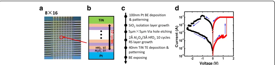
In this study, an 8 × 16 RRAM crossbar array with cell structure Pt/Al2O3/HfO2/TiN/Al was fabricated as
shown in Fig. 1a, b. Figure 1c shows the process flow of RRAM crossbar array’s fabrication. Initially, 20 nm Ti adhesion layer and 100 nm Pt bottom electrode (BE) layer on SiO2/Si substrate are deposited by
phys-ical vapor deposition (PVD). After photolithography and lift-off, the Pt bottom electrode bars were pre-pared. Then, plasma-enhanced chemical vapor depos-ition (PECVD) was used to fabricate 20-nm SiO2
isolation layer. After that, 5 μm × 5 μm via holes through the isolation layer were formed by reactive ion etching (RIE), and the resistive switching layer was deposited by ALD. The multi-layer Al2O3/HfO2,
stacked as resistive switching layer, was deposited with a total thickness of 5 nm. Controlling the resistive switching layer precisely by ALD is beneficial to achieve high switching uniformity [21]. Then, 40 nm TiN and 100 nm Al top electrode (TE) layers were * Correspondence:[email protected]
Institute of Microelectronics, Peking University, Beijing 100871, China
sputtered and patterned by photolithography. The last process was dry etching, in order to expose the Pt bot-tom electrode pad. Agilent B1500A semiconductor parameter analyzer and Agilent 81160A pulse gener-ator were used for the electrical measurement.
Results and discussion
After forming operation, the SET/RESET bias voltage (swept from 0 to +2.5/−2.5 V, then back to 0 V) was ap-plied to the TE, with the BE grounded. The typical DC current–voltage (I–V) characteristics are shown in Fig. 1d. The devices show bipolar resistive switching be-havior with abrupt SET process from high-resistance state (HRS) to low-resistance state (LRS) and gradual RESET process from LRS to HRS. As shown in Fig. 2, multilevel resistance states can be achieved by control-ling the current compliance value during SET and modulating stop voltage during RESET. The achieved multilevel resistance states show the devices’robustness to the disturb pulses during SET and RESET, as shown in Fig. 3. These multilevel resistance states reached by SET and RESET will enable the realization of binary STDP protocol.
A binary STDP protocol is proposed and demon-strated as shown in Fig. 4. The time overlap between the pre-pulse at the TE and the post-pulse at the BE leads to a change of the device conductance. The par-ameter delta t (Δt) is defined as Δt=tpost−tpre, where
tpost is the time when post-pulse arrived BE andtpreis the time when pre-pulse arrived TE. Figure 4a is the wave-forms used in the protocol. It includes two pre-pulses (pre I and pre II) and one post-pulse (post). For the conveni-ence of displaying, we set the time span of post as 2μs. WithΔtvarying from−1000 ns to 3000 ns, only when the pre I meets the post betweent1andt2(Fig. 4b) could the RRAM device be switched to LRS, which corresponds to long-term potentiation (LTP). If the pre II meets the post between t2 and t3 (Fig. 4c), the RRAM device will be switched to HRS, which corresponds to long-term depression (LTD). In other situations, the super imposed waveforms will not switch resistance states. In the proto-col, LTP and LTD are determined by the type of pre and delta t. For different initial resistance states (from about 4 × 10²Ω to 4 × 10⁴Ω), the device performs similar switching behavior.
a
b
c
d
Fig. 1aMicroscope image of the fabricated 8 × 16 Al2O3/HfO2-based crossbar RRAM array.bThe structure of RRAM cell.cThe fabrication process flow.dTypical I–V curve measured in the RRAM cells
a
b
Fig. 2Measured multilevel resistance states characteristics of the cells in the crossbar RRAM arrays.aUsing current sweeping mode for SET.bUsing voltage sweeping mode for RESET
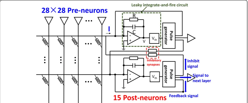
[image:2.595.59.539.87.201.2] [image:2.595.306.539.547.693.2] [image:2.595.57.293.571.692.2]An unsupervised online learning system (Fig. 5) con-sists of 28 × 28 pre-neurons, and 15 post-neurons are de-signed based on the binary STDP protocol above, with RRAM cells working as synapses. Leaky integrate-and-fire (LIF) circuits and pulse generators were adopted to construct the post-neurons. Pre-neurons are fully con-nected with post-neurons by the crossbar structure. Be-sides, post-neurons connect to each other through inhibitory synapses. In post-neuron, the LIF circuit col-lects currents from synapses which are connected to it. The LIF circuit integrates the currents and intrigues the pulse generators when the internal potential exceeds a fixed threshold. The fired pulse generators will generate three signals: the feedback signal, the inhibiting signal, and the signal for the next layer. The feedback signal is used to update synapse weights. The inhibiting signal can inhibit other neurons by inhibitory synapses. The signal for the next layer shows the recognition results.
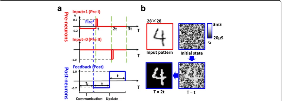
Training session and test session are two main sessions for a pattern recognition system. At training session, learn-ing events occur at discrete time periods (learnlearn-ing epochs). In this system, the implementation of training session is as follows. Before training session, all synaptic weights were initially set to random values, with an expected valueGE= 0.5 × (GLRS+GHRS), whereGLRSis the conductance of LRS andGHRSis the conductance of HRS. At the beginning of one learning epoch, handwritten 2D digit patterns from MNIST database are converted into one dimension binary input information. Corresponding to input 1/0, pre-neurons input pre I/pre II into the system (Fig. 6a). During communication stage (from 0 to 1), the pre I/pre II voltage was set to −0.2 V/0 V. Post-neuron which has maximum sum of current will fire first. The fired neuron reduces sum currents of other neurons by the inhibiting signal and thus becomes the only fired neuron. At the same time, the fired neuron sends a feedback signal (post) to the connected Fig. 4A binary STDP protocol.aWaveforms used in this protocol. Including pre I, pre II, and post.b,cMeasured binary STDP characteristics. LTP and LTD are determined by pre type and deltat
[image:3.595.57.539.88.209.2] [image:3.595.57.540.492.692.2]synapses (Fig. 6a). The post consists of a negative pulse (−0.7 V, t s) and a positive pulse (1.0 V, t s). The post encounters the pre I and the pre II at the synapses which are connected to the fired neuron. According to binary STDP protocol, LTP/LTD can only be achieved at synapses connecting the fired neuron, corresponding to the pre I/pre II at the timet/2t, and thus, other synapses are not affected. The evolution of the synaptic weight maps is shown in Fig. 6b. Through one learning epoch, the input information is stored into the synapses which are connected to the fired neuron. Afterwards, another learning epoch follows. The training session is over when all learning epochs are completed.
In the system, the time tf which is needed to fire a post-neuron is determined by the input current I, the RC parameter of the integrating circuit, and the thresh-old voltage Vth tf ¼−RC ln IRVþth1
. The input current
is related to the input information and synaptic weights. For a constant threshold voltage, a higher input current leads to a shorter tf. As a result, communication stage
should be wide enough in order that all input informa-tion can fire a post-neuron. In our simulainforma-tion, we pre-sume that our circuit works at an ideal state; hence, parametertcan be considered an ideal value. In order to update weights at various fire time, the time span be-tween the input waveform and the feedback waveform should be 2t.
A learning and classification task of ten patterns is used to verify the function of this system. The weight maps after training session are shown in Fig. 7. Ten-digit patterns fired ten different post-neurons randomly, which shows that patterns are learned and classified successfully.
Conclusions
A RRAM-based binary STDP protocol was proposed and experimentally demonstrated in a RRAM-based crossbar array. An unsupervised online pattern recogni-tion system is designed to demonstrate the protocol. The simulations indicate that the system can efficiently learn and classify the handwritten digit patterns from MNIST database, which suggests that the RRAM-based binary STDP protocol is a potential learning approach that can be used for brain-inspired computing systems.
Acknowledgements
This work was supported in part by the NSFC (61334007, 61421005, and 61604005), Beijing Municipal Science and Technology Plan Projects.
Authors’Contributions
ZZ proposed the binary STDP protocol, carried out measurement with the assistance of WS, simulated the network, and drafted the manuscript under the instruction of XL, LL, PH, and JK. CL and PH provided useful suggestions for the measurement design. ZD and ZC modified the grammar. JK supervised the work and finalized the manuscript. All authors read and approved the final manuscript.
Competing Interests
The authors declare that they have no competing interests.
a
b
Fig. 6One learning epoch.aWaveforms used for the learning epoch, including pre I, pre II and post, which correspond to input information 0, 1, and feedback signal. Parametertfmeans integrating time required to fire post-neuron.bThe evolution of synaptic weights map.Blackpixels and
whitepixels learned at timetand 2t, respectively
[image:4.595.58.540.88.262.2] [image:4.595.58.292.585.705.2]Manohar R, Risk WP, Jackson B, Modha DS (2015) TrueNorth: design and tool flow of a 65 mW 1 million neuron programmable neurosynaptic chip. IEEE Trans Comput Aided Des Integr Circuits Syst 34(10):1537–1557 2. Furber SB, Galluppi F, Temple S, Plana LA (2014) The spinnaker project. Proc
IEEE 102(5):652–665
3. Schemmel J, Fieres J, Meier K (2008) Wafer-scale integration of analog neural networks. In 2008 IEEE International Joint Conference on Neural Networks (IEEE World Congress on Computational Intelligence), 2008, June. IEEE, Hong Kong, pp 431–438
4. Ambrogio S, Ciocchini N, Laudato M, Milo V, Pirovano A, Fantini P, Ielmini D (2016) Unsupervised learning by spike timing dependent plasticity in phase change memory (PCM) synapses. Frontiers in neuroscience 10:56 5. Kaneko Y, Nishitani Y, Ueda M (2014) Ferroelectric artificial synapses for
recognition of a multishaded image. IEEE Trans Electron Devices 61(8):2827–2833 6. Gao B, Bi Y, Chen HY, Liu R, Huang P, Chen B, Liu LF, Liu XY, Yu S, Wong
HSP, Kang J (2014) Ultra-low-energy three-dimensional oxide-based electronic synapses for implementation of robust high-accuracy neuromorphic computation systems. ACS Nano 8(7):6998–7004 7. Yu S, Gao B, Fang Z, Yu H, Kang J, Wong HSP (2013) A low energy
oxide-based electronic synaptic device for neuromorphic visual systems with tolerance to device variation. Adv Mater 25(12):1774–1779
8. Zhang W, Hu Y, Chang TC, Chang KC, Tsai TM, Chen HL, Su YT, Chu TJ, Chen MC, Huang HC, Su WC, Zheng JC, Hung YC, Su WC (2015) An electronic synapse device based on solid electrolyte resistive random access memory. IEEE Electron Device Lett 36(8):772–774
9. Park S., Kim H., Choo M., Noh J., Sheri A., Jung S., Seo K., Park J., Kim S., Lee W., Shin J., Lee D., Choi G., Woo J., Cha E., Jang J., Park C., Jeon M., Lee B., Lee H., Hwang H.: RRAM-based synapse for neuromorphic system with pattern recognition function. In: Proceedings of the 2012 IEEE International Electron Devices Meeting (IEDM), December, (pp. 1–10)
10. Chen Z, Gao B, Zhou Z, Huang P, Li H, Ma W, Zhu D, Liu LF, Liu XY, Kang J, Chen HY. Optimized learning scheme for grayscale image recognition in a RRAM based analog neuromorphic system. In: Proceedings of the 2015 IEEE International Electron Devices Meeting (IEDM), Washington, DC, pp. 17.7.1–17.7.4 11. Govoreanu B., Kar G. S., Chen Y. Y., Paraschiv V., Kubicek S., Fantini A., Radu I.P.,
Goux L., Clima S., Degraeve R., Jossart N., Richard O., Vandeweyer T., Seo K., Hendrickx P., Pourtois G., Bender H., Altimime L., Wouters D.J., Kittl J.A., Jurczak M.: 10× 10nm 2 Hf/HfO x crossbar resistive RAM with excellent performance, reliability and low-energy operation. In: Proceedings of the 2011 IEEE International Electron Devices Meeting (IEDM), December (pp. 31–6) 12. Yu S, Chen HY, Gao B, Kang J, Wong HSP (2013) HfOx-based vertical
resistive switching random access memory suitable for bit-cost-effective three-dimensional cross-point architecture. ACS Nano 7(3):2320–2325 13. Wang I. T., Lin Y. C. Wang Y. F., Hsu C. W., Hou T. H.: 3D synaptic
architecture with ultralow sub-10 fJ energy per spike for neuromorphic computation. In: Proceedings of the 2014 IEEE International Electron Devices Meeting (IEDM), December (pp. 28–5)
14. Huang P, Chen S, Zhao Y, Chen B, Gao B, Liu LF, Chen Y, Zhang Z, Bu W, Wu H, Liu XY, Kang JF (2016) Self-selection RRAM cell with sub-μA switching current and robust reliability fabricated by high-K/metal gate CMOS compatible technology. IEEE Trans Electron Devices 63(11):4295–4301 15. Huang P, Kang J, Zhao Y, Chen S, Han R, Zhou Z, Chen Z, Ma W, Li M, Liu
LF, Liu XY (2016) Reconfigurable nonvolatile logic operations in resistance switching crossbar array for large‐scale circuits. Adv Mater 28(44):9758–9764 16. Yu S, Wu Y, Jeyasingh R, Kuzum D, Wong HSP (2011) An electronic synapse device based on metal oxide resistive switching memory for neuromorphic computation. IEEE Trans Electron Devices 58(8):2729–2737
17. Wang Z, Ambrogio S, Balatti S, Ielmini D (2015) A 2-transistor/1-resistor artificial synapse capable of communication and stochastic learning in neuromorphic systems. Frontiers in neuroscience 8:438
21. Chen Z, Zhang F, Chen B, Zheng Y, Gao B, Liu LF, Liu XY, Kang JF (2015) High-performance HfO x/AlO y-based resistive switching memory cross-point array fabricated by atomic layer deposition. Nanoscale Res Lett 10(1):1
Submit your manuscript to a
journal and benefi t from:
7Convenient online submission 7Rigorous peer review
7Immediate publication on acceptance 7Open access: articles freely available online 7High visibility within the fi eld
7Retaining the copyright to your article