Implementation of High Speed Full Adder Using
DTMOS
Shubham Bansal1, Dr. Neelam R. Prakash2
1(M.E. Student) ECE Department PEC University of Technology Chandigarh, India 2Professor, ECE Department PEC University of Technology Chandigarh, India
Abstract: The power dissipation is a major problem in electronic devices. The importance for Power Management Integrated Circuit (PMIC) is emphasized as battery-powered portable electronics such as smart phone are commonly used. DTMOS technique meets the requirement for the low voltage and high-speed circuits. Due to larger current driving capacity and low leakage current, DTMOS is attractive for low power applications. So in this paper full adder design has been implemented using DTMOS technology and calculated its power dissipation and delay and compare this adder with CMOS adder using cadence tool.
Keywords – Full Adder, DTMOS, Low Power, CMOS
I. INTRODUCTION
The market demand for transferable and efficient electronic devices have pushed the industry to intend chip with high compactness, low power consumption and better performance. To obtain these goals the technology range of the CMOS has to face constant downscaling. As the technology is being reduced day by day with the reduction of channel size i.e. length of the MOSFET, the other parameter dimensions also need to be minimized. For analog and digital circuits, it is an important part to make circuits that consume less power. By using existing design methodology to make low power circuits, the applied voltage at least should be equal to the sum of threshold voltage of n-type and p-type circuits.
In DTMOS technique bulk terminal is connected to the gate terminal is a capable method for achieving superior performance without even modifying the present configuration of MOSFET. This is the chief advantage of DTMOS as it is fully compatible with the conventional CMOS process.
In this paper an adder has been implemented that is one of the most important apparatus of a central processing unit. Because it is not only used in adding of bits but also in several other processes like address calculation, subtraction, division and multiplication. The adders are very important part of circuits because they used to determine the speed, delay and power of the systems so adders that consume less power are always preferable. A single-bit full adder can be fully characterized by the below equations:
A
B
C
inSum
inout
A
B
A
B
C
C
The rest of the paper is organized as follows. An overview of the DTMOS technology which has been using in the implementation of full adder is in section II. A full adder circuit using DTMOS is presented in section III. Simulation results are presented in section IV. Conclusion remarks are given in section V.
II. OVERVIEWOFDTMOSTECHNOLOGY
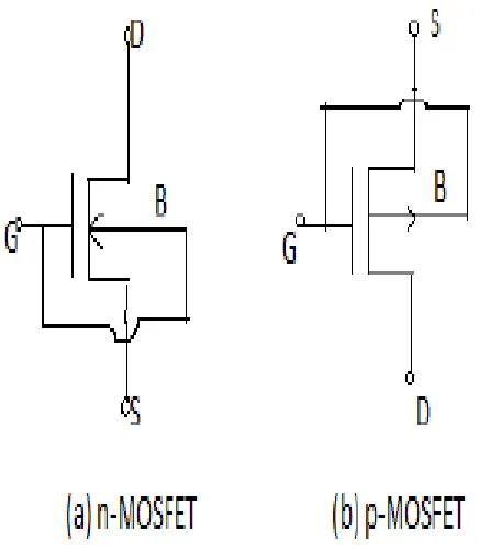
The DTMOS technique was first invented in 1994. As there are several circuit applications that have been designed till now. But the DTMOS technique is mainly used technique in digital circuits in which MOSFET’s gate and body are tied together. As it has very great advantage of MOSFET as it reduces the leakage current and provides high threshold voltage during off state and shows low threshold voltage during on state to increase the current driving capabilities of the circuit. This technique can also be used in bulk CMOS technology for applications of analog circuit. However, in analog circuits body terminal of the MOSFET transistor is used as a forth terminal.
©IJRASET: All Rights are Reserved
[image:3.612.194.412.130.385.2]1625
minimizes. DTMOS provides less delay with increased speed, hence it is a great technique than traditional body biasing in the sub-threshold region.Figure 1: DTMOS Structure
Figure 2 shows the schematic of DTCMOS inverter. Due to the body effect, during the different modes of operation, threshold voltage of DTMOS can be altered accordingly. When input supply ‘IN’ is grounded, PMOS is in ‘ON’ state with low Vth and with
regular Vth NMOS is in ‘OFF’ state. As due to low Vth of PMOS, it works in active mode operation and the circuit goes from low to
[image:3.612.165.443.528.706.2]high with lesser propagation delay. When IN is connected to supply voltage exactly opposite situation takes place. As diode circuit’s built-in potential limits the supply voltage of DTMOS. So for low voltages (0.6-V and below), this technique can be used with higher speed.
III. FULLADDERUSINGDTMOSTECHNOLOGY
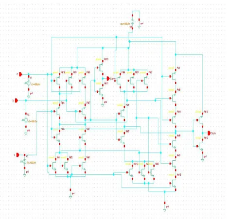
The adder is one of the most basic parts of a processor circuit, as Arithmetic Logic Unit (ALU), floating-point unit contains the adder circuit. Adder circuit also uses for address calculation in cache or memory access applications. With Increase in demand for low power and portable electronic devices such as mobile phones and laptop computers needs power efficient VLSI circuits. of NMOS and PMOS transistor cells are being used to build this adder cell. To realize the full adder circuit logic equation (1) and logic equation (2) is used and convert these equations directly into CMOS circuit.
Cout = A.B + A.Cin + B.Cin …….. (1)
[image:4.612.82.549.194.645.2]SUM = A.B.Cin + Cout (A + B + Cin) ……. (2)
Figure 3: Conventional CMOS Full Adder
©IJRASET: All Rights are Reserved
[image:5.612.81.547.73.355.2]1627
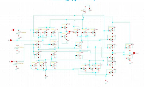
Figure 4:Proposed Full Adder using DTMOS TechnologyIV. SIMULATIONANDRESULT
The 1-bit full adder has been simulated at 180nm technology. Cadence Virtuoso software platform is use to perform the circuits. The Input voltage (Vdd) of 0.6 and 0.4 is applied for the conventional CMOS and proposed DTMOS full adder circuits. The comparison
results of DTMOS and CMOS have been shown in Table 1.
Table -1 Simulation Result: Show the comparison of Average Power, Propagation Delay and Power delay Product of 28T adder circuit using DTMOS and CMOS technology.
Technology Voltage
(Vdd)
PARAMETERS Average Power (Microwatt) Delay (nanoseconds) Power Delay Product(in femto)
DTMOS 0.6V 204.1 8.862 1808.73
DTMOS 0.4V .6698 19.89 13.322
CMOS 0.6V .3115 149.0 464.135
CMOS 0.4V .04316 45.78 19.7586
As from results shown in Table 1, DTMOS shows lesser delay and delay power product but it consumes more power as compared to CMOS. Hence to get lesser delay with more speed as compared to traditional body biasing scheme, DTMOS is a great and efficient scheme. While Operating at lower voltages, Dynamic threshold MOS (DTMOS) circuits provide high current driving capabilities and low leakage power as compared to CMOS circuits,.
V. CONCLUSION
[image:5.612.35.523.470.581.2]REFERENCES
[1] Fariborz Assaderaghi,Stephen Parke,Dennis Sinitsky,Jeffrey Bokor,Ping K. Ko, Chenming Hu, “A Dynamic Threshold Voltage MOSFET (DTMOS) for Very Low Voltage Operation”, IEEE Electron Device Letters,Vo1. 15,NO. 12,December 1994.
[2] Mohammad Maymandi-Nejad, Manoj Sachdev, "DTMOS Technique for Low-Voltage Analog Circuits," IEEE Transactions On Very Large Scale Integration (VLSI) Systems, VOL. 14, NO. 10, OCTOBER 2006.
[3] Sonam, Asst. Prof. Richa srivastava, "Dynamic Threshold MOS (DTMOS) and its applications," International Journal of Science, Engineering and Technology Research (IJSETR) Volume 5, Issue 6, June 2016.
[4] Ch. Ashok Babu, J.V.R. Ravindra, K. Lal Kishore, " An Adder with Novel PMOS and NMOS for Ultra Low Power Applications in Deep Submicron Technology ", Global Journal of Researches in Engineering Electrical and Electronics Engineering Volume 13 Issue 14 Version 1.0 Year 2013.