Advances in Radio Science (2004) 2: 215–219
© Copernicus GmbH 2004
Advances in
Radio Science
Power estimation on functional level for programmable processors
M. Schneider, H. Blume, and T. G. Noll
Lehrstuhl f¨ur Allgemeine Elektrotechnik und Datenverarbeitungssysteme, RWTH Aachen, Schinkelstraße 2, 52062 Aachen, Germany
Abstract. In diesem Beitrag werden verschiedene Ans¨atze zur Verlustleistungssch¨atzung von programmierbaren Prozessoren vorgestellt und bez¨uglich ihrer ¨Ubertragbarkeit auf moderne Prozessor-Architekturen wie beispielsweise Very Long Instruction Word (VLIW)-Architekturen be-wertet. Besonderes Augenmerk liegt hierbei auf dem Konzept der sogenannten Functional-Level Power Analy-sis (FLPA). Dieser Ansatz basiert auf der Einteilung der Prozessor-Architektur in funktionale Bl¨ocke wie beispiel-sweise Processing-Unit, Clock-Netzwerk, interner Speicher und andere. Die Verlustleistungsaufnahme dieser Bl¨ocke wird parameterabh¨angig durch arithmetische Modellfunk-tionen beschrieben. Durch automatisierte Analyse von Assemblercodes des zu sch¨atzenden Systems mittels eines Parsers k¨onnen die Eingangsparameter wie beispielsweise der erzielte Parallelit¨atsgrad oder die Art des Speicherzu-griffs gewonnen werden. Dieser Ansatz wird am Beispiel zweier moderner digitaler Signalprozessoren durch eine Vielzahl von Basis-Algorithmen der digitalen Signalver-arbeitung evaluiert. Die ermittelten Sch¨atzwerte f¨ur die einzelnen Algorithmen werden dabei mit physikalisch gemessenen Werten verglichen. Es ergibt sich ein sehr kleiner maximaler Sch¨atzfehler von 3%.
In this contribution different approaches for power esti-mation for programmable processors are presented and eval-uated concerning their capability to be applied to modern digital signal processor architectures like e.g. Very Long In-struction Word (VLIW) -architectures. Special emphasis will be laid on the concept of so-called Functional-Level Power Analysis (FLPA). This approach is based on the separation of the processor architecture into functional blocks like e.g. processing unit, clock network, internal memory and others. The power consumption of these blocks is described by pa-rameter dependent arithmetic model functions. By applica-tion of a parser based automized analysis of assembler codes of the systems to be estimated the input parameters of the
Correspondence to: H. Blume
arithmetic functions like e.g. the achieved degree of paral-lelism or the kind and number of memory accesses can be computed. This approach is exemplarily demonstrated and evaluated applying two modern digital signal processors and a variety of basic algorithms of digital signal processing. The resulting estimation values for the inspected algorithms are compared to physically measured values. A resulting maxi-mum estimation error of 3% is achieved.
1 Introduction
In the course of increasing complexity of digital signal pro-cessing applications, especially in the field of mobile ap-plications, low power techniques are of crucial importance. Therefore, it is desirable to estimate the power consumption of a system at a very early stage in the design flow. By this means it is possible to predict whether a system will meet a certain power budget before it is physically implemented. Necessary changes in the system partitioning or the underly-ing architecture will then be much less time and money con-suming, because no physical implementation of the system is required to determine its power dissipation.
Another important design criteria of modern electronic systems is the demand for flexibility, e.g. the ability to adapt a system to changing specifications or standards. This fact along with the continuous growth of their computa-tional power makes programmable digital signal processor (DSP)-kernels a very attractive component for heterogeneous Systems-on-Chip.
216 M. Schneider et al.: Power estimation on functional level for programmable processors
paper and verified using several exemplary vehicles. The paper is organized as follows: Chapter 2 shortly reviews
and discusses several existing power estimation techniques in terms of their portability to modern DSP
architec-tures. The following chapter describes the so-called Functional-Level Power Analysis (FLPA) approach in detail.
Chapter 4 lists some results concerning the application of the FLPA methodology for estimating the power of a
variety of basic algorithms. A conclusion of the paper is given in chapter 5.
2 Classical approaches for power estimation
One possible straight forward power estimation approach on DSPs is the so-called Physical-Level Power
Analysis methodology. This approach is based on the analysis of the switching activity of all transistors of the
DSP architecture. The requirement of this methodology is the availability of a description of the processor
architecture on the transistor level, which is rarely given for modern DSPs. But the main disadvantage is the
extremely high computational effort that makes approaches like this inapplicable for digital signal processors.
Architectural-Level approaches like (Brooks, D., et al.; 2000) reduce this computational effort by modelling
typical architecture elements like registers, functional units or load/store queues. These models are not based on
physical measurements and require still exact knowledge of the processors architecture. Therefore, these two
methodologies can be mainly found in the field of microprocessor development.
Another possibility for power estimation for DSPs is the so-called Instruction-Level Power Analysis
(Tiwari, V., et al.; 1996). By means of physical measurements or low level simulations the energy consumption of
each instruction out of the instruction set of a given processor is determined. By analysis of the assembler code of
a program it is then possible to estimate the specific power consumption for this program performed on a certain
processor. The advantage of this approach is the ability to cover a specific part of power consumption of DSPs:
the so-called inter-instruction effects. In general, the energy consumption of a DSP instruction depends on the
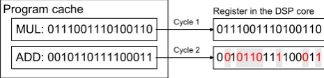
previously executed instructions, what can be explained by means of Figure 1 and Figure 2.
Program cache
MUL: 0111001110100110 ADD: 0010110111100011
0111001110100110 0010110111100011
Cycle 1
Cycle 2
Register in the DSP core
Figure 1. Sequential execution of two different DSP instructions
Program cache
ADD: 0010110111100011
0111001110100110
Cycle 1
Cycle 2
Register in the DSP core
ADD: 0010110111100011
0111001110100110
Figure 2. Sequential execution of two identical DSP instructions
At a certain stage of a processors pipeline, instruction words are transferred from the program cache into a
register in the DSP core for further processing. Figure 1 shows the situation that an ADD (addition) instruction
word replaces a MUL (multiplication) instruction word in cycle 2. The numbers shaded with gray boxes show the
bits in the register that switch their state in this case. In this example a Hamming distance (number of different
bits of these two instruction words) of eight (
H
d=8) is resulting. As can be seen in Figure 2 the sequence of two
identical instructions causes no switching activity (
H
d=0). Effects like this occur in many stages of a processors
pipeline and as a result of these effects the energy consumption of a DSP instruction obviously depends on the
previously executed instruction (Marwedel, P.; 2003). The Instruction-Level Power Analysis methodology allows
to cover such inter-instruction effects by measuring the energy consumption of groups of DSP instructions, but
that makes this approach very complex due to the huge number of possible combinations. The effort will even
grow, if Very-Long-Instruction-Word (VLIW) architectures shall be modeled due to their increasing word length
and their ability to issue several operations in parallel.
A more attractive approach for power estimation is the Functional-Level Power Analysis (FLPA) methodology.
This methodology has been introduced in (Qu, G., et al.; 2000) and was first applied in (Senn, E., et al.; 2002) to
a digital signal processor. Here, a refined extension of this methodology is presented in order to model complete
DSP cores including the modeling of separate units like cache, internal RAM, EDMA and integrated
co-processors, different types of memory accesses etc. The following section will demonstrate this methodology
applying an exemplary vehicle – the TMS320C6416 DSP.
3 Functional-Level Power Analysis (FLPA)
The basic principle of the FLPA methodology is depicted in Figure 3.
Fig. 1. Sequential execution of two different DSP instructions.programming styles or the choice of algorithmic alternatives which all strongly influence the power consumption of an al-gorithm that is executed on a DSP.
For this reason it is desirable to consider methodologies for power estimation that cover all significant influencing factors and provide a sufficient accuracy at moderate com-plexity. Such a methodology is presented in this paper and verified using several exemplary vehicles. The paper is orga-nized as follows: Sect. 2 shortly reviews and discusses sev-eral existing power estimation techniques in terms of their portability to modern DSP architectures. The following sec-tion describes the so-called Funcsec-tional-Level Power Analy-sis (FLPA) approach in detail. Section 4 lists some results concerning the application of the FLPA methodology for es-timating the power of a variety of basic algorithms. A con-clusion of the paper is given in Sect. 5.
2 Classical approaches for power estimation
One possible straight forward power estimation approach on DSPs is the so-called Physical-Level Power Analysis methodology. This approach is based on the analysis of the switching activity of all transistors of the DSP architecture. The requirement of this methodology is the availability of a description of the processor architecture on the transistor level, which is rarely given for modern DSPs. But the main disadvantage is the extremely high computational effort that makes approaches like this inapplicable for digital signal pro-cessors. Architectural-Level approaches like (Brooks et al., 2000) reduce this computational effort by modelling typi-cal architecture elements like registers, functional units or load/store queues. These models are not based on physical measurements and require still exact knowledge of the pro-cessors architecture. Therefore, these two methodologies can be mainly found in the field of microprocessor development. Another possibility for power estimation for DSPs is the so-called Instruction-Level Power Analysis (Tiwari et al., 1996). By means of physical measurements or low level sim-ulations the energy consumption of each instruction out of the instruction set of a given processor is determined. By analysis of the assembler code of a program it is then possi-ble to estimate the specific power consumption for this pro-gram performed on a certain processor. The advantage of this approach is the ability to cover a specific part of power consumption of DSPs: the so-called inter-instruction effects. In general, the energy consumption of a DSP instruction
de-paper and verified using several exemplary vehicles. The de-paper is organized as follows: Chapter 2 shortly reviews
and discusses several existing power estimation techniques in terms of their portability to modern DSP
architec-tures. The following chapter describes the so-called Functional-Level Power Analysis (FLPA) approach in detail.
Chapter 4 lists some results concerning the application of the FLPA methodology for estimating the power of a
variety of basic algorithms. A conclusion of the paper is given in chapter 5.
2 Classical approaches for power estimation
One possible straight forward power estimation approach on DSPs is the so-called Physical-Level Power
Analysis methodology. This approach is based on the analysis of the switching activity of all transistors of the
DSP architecture. The requirement of this methodology is the availability of a description of the processor
architecture on the transistor level, which is rarely given for modern DSPs. But the main disadvantage is the
extremely high computational effort that makes approaches like this inapplicable for digital signal processors.
Architectural-Level approaches like (Brooks, D., et al.; 2000) reduce this computational effort by modelling
typical architecture elements like registers, functional units or load/store queues. These models are not based on
physical measurements and require still exact knowledge of the processors architecture. Therefore, these two
methodologies can be mainly found in the field of microprocessor development.
Another possibility for power estimation for DSPs is the so-called Instruction-Level Power Analysis
(Tiwari, V., et al.; 1996). By means of physical measurements or low level simulations the energy consumption of
each instruction out of the instruction set of a given processor is determined. By analysis of the assembler code of
a program it is then possible to estimate the specific power consumption for this program performed on a certain
processor. The advantage of this approach is the ability to cover a specific part of power consumption of DSPs:
the so-called inter-instruction effects. In general, the energy consumption of a DSP instruction depends on the
previously executed instructions, what can be explained by means of Figure 1 and Figure 2.
Program cache
MUL: 0111001110100110 ADD: 0010110111100011
0111001110100110 0010110111100011
Cycle 1
Cycle 2
Register in the DSP core
Figure 1. Sequential execution of two different DSP instructions
Program cache
ADD: 0010110111100011
0111001110100110
Cycle 1
Cycle 2
Register in the DSP core
ADD: 0010110111100011
0111001110100110
Figure 2. Sequential execution of two identical DSP instructions
At a certain stage of a processors pipeline, instruction words are transferred from the program cache into a
register in the DSP core for further processing. Figure 1 shows the situation that an ADD (addition) instruction
word replaces a MUL (multiplication) instruction word in cycle 2. The numbers shaded with gray boxes show the
bits in the register that switch their state in this case. In this example a Hamming distance (number of different
bits of these two instruction words) of eight (
H
d=8) is resulting. As can be seen in Figure 2 the sequence of two
identical instructions causes no switching activity (
H
d=0). Effects like this occur in many stages of a processors
pipeline and as a result of these effects the energy consumption of a DSP instruction obviously depends on the
previously executed instruction (Marwedel, P.; 2003). The Instruction-Level Power Analysis methodology allows
to cover such inter-instruction effects by measuring the energy consumption of groups of DSP instructions, but
that makes this approach very complex due to the huge number of possible combinations. The effort will even
grow, if Very-Long-Instruction-Word (VLIW) architectures shall be modeled due to their increasing word length
and their ability to issue several operations in parallel.
A more attractive approach for power estimation is the Functional-Level Power Analysis (FLPA) methodology.
This methodology has been introduced in (Qu, G., et al.; 2000) and was first applied in (Senn, E., et al.; 2002) to
a digital signal processor. Here, a refined extension of this methodology is presented in order to model complete
DSP cores including the modeling of separate units like cache, internal RAM, EDMA and integrated
co-processors, different types of memory accesses etc. The following section will demonstrate this methodology
applying an exemplary vehicle – the TMS320C6416 DSP.
3 Functional-Level Power Analysis (FLPA)
The basic principle of the FLPA methodology is depicted in Figure 3.
Fig. 2. Sequential execution of two identical DSP instructions.
pends on the previously executed instructions, what can be explained by means of Figs. 1 and 2.
At a certain stage of a processors pipeline, instruction words are transferred from the program cache into a register in the DSP core for further processing. Figure 1 shows the situation that an ADD (addition) instruction word replaces a MUL (multiplication) instruction word in cycle 2. The numbers shaded with gray boxes show the bits in the reg-ister that switch their state in this case. In this example a Hamming distance (number of different bits of these two in-struction words) of eight (Hd=8) is resulting. As can be seen
in Fig. 2 the sequence of two identical instructions causes no switching activity (Hd=0). Effects like this occur in many
stages of a processors pipeline and as a result of these ef-fects the energy consumption of a DSP instruction obviously depends on the previously executed instruction (Marwedel, 2003). The Instruction-Level Power Analysis methodology allows to cover such inter-instruction effects by measuring the energy consumption of groups of DSP instructions, but that makes this approach very complex due to the huge num-ber of possible combinations. The effort will even grow, if Very-Long-Instruction-Word (VLIW) architectures shall be modeled due to their increasing word length and their ability to issue several operations in parallel.
A more attractive approach for power estimation is the Functional-Level Power Analysis (FLPA) methodology. This methodology has been introduced in (Qu et al., 2000) and was first applied in (Senn et al., 2002) to a digital sig-nal processor. Here, a refined extension of this methodol-ogy is presented in order to model complete DSP cores in-cluding the modeling of separate units like cache, internal RAM, EDMA and integrated co-processors, different types of memory accesses etc. The following section will demon-strate this methodology applying an exemplary vehicle – the TMS320C6416 DSP.
3 Functional-Level Power Analysis (FLPA)
The basic principle of the FLPA methodology is depicted in Fig. 3.
M. Schneider et al.: Power estimation on functional level for programmable processors 217
Task architectureDSP
Compilation
Parameter Extraction
FLPA
Measurements
Power Model
Task
Parameters ArithmeticModels
Estimated Power Consumption
Figure 3. The basic FLPA principle
In a first step the DSP architecture is divided into functional blocks like fetch unit, processing unit, internal memory and others like the clocking system. By means of measurements it is possible to find an arithmetic function for each block that determines its power consumption in dependency of certain parameters. These parameters are for example the clock frequency, the degree of parallelism or the rate with which the internal memory is accessed. Most of these parameters can be automatically determined by a parser which analyzes the assembler file of a program code. The total power consumption is then given as the sum of the power consump-tion of each funcconsump-tional block:
∑
=
i i block total P
P . (1)
The left side of Figure 3 depicts the process of extracting parameters from a program which implements a task. After compilation it is possible to extract the task parameters from the assembler code. Further parameters can be derived from a single execution of the program (e.g. the number of required clock cycles). These parameters are the input values for the previously determined arithmetic model functions. Thus, an estimation for the algorithms power consumption can be computed. This approach is applicable to all kinds of processor architectures. Further on, FLPA can be applied to a processor with moderate effort and no detailed knowledge of the processors architecture is necessary.
3.1 An exemplary vehicle: The TMS320C6416 DSP
The TMS320C6416 is a state-of-the-art VLIW DSP aiming for multimedia applications. Figure 4 depicts a block diagram of the DSP architecture.
Datapath A
L1 S1 M1 D1
Register bank A A31 - A0
Datapath B
D2 S2 M2 L2
Register bank B B31 - B0 Fetch VLIW instruction word Dispatch atomic instructions
Level 1 Program Cache
Level 1 Data Cache Viterbi-CP
Turbo-CP
Leve
l2
S
R
A
M
,Le
vel
2
C
ach
e
EDMA
In
te
rf
a
ce
s, P
er
iph
er
al
s
Figure 4. The TMS320C6416 architecture
Fig. 3. The basic FLPA principle.
Task architectureDSP
Compilation
Parameter Extraction
FLPA
Measurements
Power Model
Task Parameters
Arithmetic Models
Estimated Power Consumption
Figure 3. The basic FLPA principle
In a first step the DSP architecture is divided into functional blocks like fetch unit, processing unit, internal memory and others like the clocking system. By means of measurements it is possible to find an arithmetic function for each block that determines its power consumption in dependency of certain parameters. These parameters are for example the clock frequency, the degree of parallelism or the rate with which the internal memory is accessed. Most of these parameters can be automatically determined by a parser which analyzes the assembler file of a program code. The total power consumption is then given as the sum of the power consump-tion of each funcconsump-tional block:
∑
=
i i block
total P
P . (1)
The left side of Figure 3 depicts the process of extracting parameters from a program which implements a task. After compilation it is possible to extract the task parameters from the assembler code. Further parameters can be derived from a single execution of the program (e.g. the number of required clock cycles). These parameters are the input values for the previously determined arithmetic model functions. Thus, an estimation for the algorithms power consumption can be computed. This approach is applicable to all kinds of processor architectures. Further on, FLPA can be applied to a processor with moderate effort and no detailed knowledge of the processors architecture is necessary.
3.1 An exemplary vehicle: The TMS320C6416 DSP
The TMS320C6416 is a state-of-the-art VLIW DSP aiming for multimedia applications. Figure 4 depicts a block diagram of the DSP architecture.
Datapath A
L1 S1 M1 D1
Register bank A A31 - A0
Datapath B
D2 S2 M2 L2
Register bank B B31 - B0 Fetch VLIW instruction word Dispatch atomic instructions
Level 1 Program Cache
Level 1 Data Cache Viterbi-CP
Turbo-CP
Leve
l2
S
R
A
M
,Le
vel
2
C
ach
e
EDMA
In
te
rf
a
ce
s, P
er
iph
er
al
s
Figure 4. The TMS320C6416 architecture
Fig. 4. The TMS320C6416 architecture.
which the internal memory is accessed. Most of these param-eters can be automatically determined by a parser which an-alyzes the assembler file of a program code. The total power consumption is then given as the sum of the power consump-tion of each funcconsump-tional block:
Ptotal= X
i
Pblocki. (1)
The left side of Fig. 3 depicts the process of extracting pa-rameters from a program which implements a task. After compilation it is possible to extract the task parameters from the assembler code. Further parameters can be derived from a single execution of the program (e.g. the number of re-quired clock cycles). These parameters are the input values for the previously determined arithmetic model functions. Thus, an estimation for the algorithms power consumption can be computed. This approach is applicable to all kinds of processor architectures. Further on, FLPA can be applied to a processor with moderate effort and no detailed knowledge of the processors architecture is necessary.
It isbased on a VLIW-architecture with two parallel data paths each including four issue-slots. Furthermore, this processor includes a couple of interfaces (ATM, PCI, etc.), an Enhanced DMA-controller (EDMA) and two dedicated co-processors (Viterbi and Turbo decoder co-processor). For this work the integrated software development environment Code Composer Studio (CCS) and the hardware test and evaluation board (TEB) including the C6416 have been utilized. For further details of this architecture see (TMS320C6416, SPRS164C documentation set).
This architecture can be divided into seven functional blocks as depicted in Figure 5.
Fetch unit
L1P read access
Instruction fetch / dispatch
Processing unit Instruction decode
Instruction execute
Internal memory L1D read access Co-processors
Viterbi CP, Turbo CP L1 Cache
L1 data read miss
L1 programm read miss
EDMA / QDMA Clock
Figure 5. Separation of the TMS320C6416 architecture into functional blocks
Arithmetic model functions describing the power consumption of a functional block can be found by means of measurements. Therefore, it is necessary to stimulate each block separately. This can be achieved by executing different parts of assembler code, that will be called scenarios according to (Senn, E., et al.; 2002).
A determination of a model function applying such scenarios will be described here considering the processing unit and the fetch unit as example.
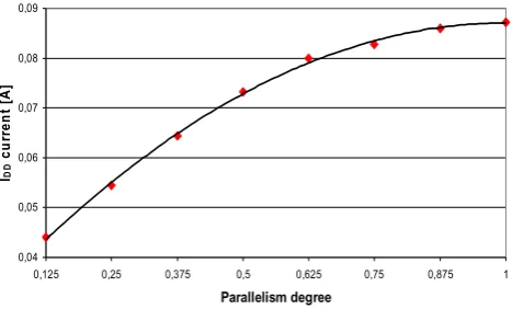
The power consumption of the processing unit has three significant parameters: • the degree of parallelism α (percentage of parallel working functional units), • the number of executed instructions,
• the type of input data.
The scenarios belonging to the processing unit vary these parameters separately.
0 0,04 0,08 0,12 0,16 0,2
0,125 0,25 0,375 0,5 0,625 0,75 0,875 1
Parallelism degree
IDD
cu
rr
en
t [A
]
worst-case complex ops (mul) 32 bit data
best-case simple ops (add) 8 bit data
typical-case 16 bit data
0 0,04 0,08 0,12 0,16 0,2
0,125 0,25 0,375 0,5 0,625 0,75 0,875 1
Parallelism degree
IDD
cu
rr
en
t [A
]
worst-case complex ops (mul) 32 bit data
best-case simple ops (add) 8 bit data
typical-case 16 bit data
Figure 6. Model function of the TMS320C6416 processing unit
In Figure 6 the current drawn by the processing unit is depicted over the degree of parallelism. The applied test scenario includes a loop where within each loop iteration 1000 instructions are executed. The dotted line of Figure 6 represents the worst-case power consumption of the processing unit, in which complex instructions (e.g. multiplications) with the maximum word length of the input data (32 bit) are executed. In contrast to that, the
Fig. 5. Separation of the TMS320C6416 architecture into
func-tional blocks.
It isbased on a VLIW-architecture with two parallel data paths each including four issue-slots. Furthermore, this processor includes a couple of interfaces (ATM, PCI, etc.), an Enhanced DMA-controller (EDMA) and two dedicated co-processors (Viterbi and Turbo decoder co-processor). For this work the integrated software development environment Code Composer Studio (CCS) and the hardware test and evaluation board (TEB) including the C6416 have been utilized. For further details of this architecture see (TMS320C6416, SPRS164C documentation set).
This architecture can be divided into seven functional blocks as depicted in Figure 5.
Fetch unit L1P read access
Instruction fetch / dispatch
Processing unit Instruction decode
Instruction execute
Internal memory L1D read access Co-processors
Viterbi CP, Turbo CP L1 Cache
L1 data read miss
L1 programm read miss
EDMA / QDMA Clock
Figure 5. Separation of the TMS320C6416 architecture into functional blocks
Arithmetic model functions describing the power consumption of a functional block can be found by means of measurements. Therefore, it is necessary to stimulate each block separately. This can be achieved by executing different parts of assembler code, that will be called scenarios according to (Senn, E., et al.; 2002).
A determination of a model function applying such scenarios will be described here considering the processing unit and the fetch unit as example.
The power consumption of the processing unit has three significant parameters: • the degree of parallelism α (percentage of parallel working functional units), • the number of executed instructions,
• the type of input data.
The scenarios belonging to the processing unit vary these parameters separately.
0 0,04 0,08 0,12 0,16 0,2
0,125 0,25 0,375 0,5 0,625 0,75 0,875 1
Parallelism degree
I
DD
cu
rr
en
t [A
]
worst-case complex ops (mul) 32 bit data
best-case simple ops (add) 8 bit data
typical-case 16 bit data
0 0,04 0,08 0,12 0,16 0,2
0,125 0,25 0,375 0,5 0,625 0,75 0,875 1
Parallelism degree
I
DD
cu
rr
en
t [A
]
worst-case complex ops (mul) 32 bit data
best-case simple ops (add) 8 bit data
typical-case 16 bit data
Figure 6. Model function of the TMS320C6416 processing unit
In Figure 6 the current drawn by the processing unit is depicted over the degree of parallelism. The applied test scenario includes a loop where within each loop iteration 1000 instructions are executed. The dotted line of Figure 6 represents the worst-case power consumption of the processing unit, in which complex instructions (e.g. multiplications) with the maximum word length of the input data (32 bit) are executed. In contrast to that, the
Fig. 6. Model function of the TMS320C6416 processing unit.
3.1 An exemplary vehicle: The TMS320C6416 DSP The TMS320C6416 is a state-of-the-art VLIW DSP aiming for multimedia applications. Figure 4 depicts a block dia-gram of the DSP architecture.
It is based on a VLIW-architecture with two parallel data paths each including four issue-slots. Furthermore, this pro-cessor includes a couple of interfaces (ATM, PCI, etc.), an Enhanced DMA-controller (EDMA) and two dedicated co-processors (Viterbi and Turbo decoder co-processor). For this work the integrated software development envi-ronment Code Composer Studio (CCS) and the hardware test and evaluation board (TEB) including the C6416 have been utilized. For further details of this architecture see (TMS320C6416, SPRS164C documentation set).
This architecture can be divided into seven functional blocks as depicted in Fig. 5.
Arithmetic model functions describing the power con-sumption of a functional block can be found by means of measurements. Therefore, it is necessary to stimulate each block separately. This can be achieved by executing different parts of assembler code, that will be called scenarios accord-ing to (Senn et al., 2002).
218 M. Schneider et al.: Power estimation on functional level for programmable processors dashed line represents the best-case power consumption with simple instructions (e.g. additions) and a small
word length of the input data (8 bit). The arithmetic function belonging to the straight line (typical-case: instruction mix, medium word length of the input data (16 bit)) is chosen as model function for the FLPA model of the TMS320C6416 processing unit and modeled by
core ,
core 2
1 2.46 10 )
10 02 . 1
( V I V
Pprocessingunit= ⋅ − ⋅α+ ⋅ − ⋅ = DD processingunit⋅ . (2)
Here, VCore denotes the core-voltage of the processing unit and α the achieved degree of parallelism. The error
of the estimated power consumption for algorithms with either extremely complex or extremely simple instruc-tions will be examined in the next section.
The architecture of the fetch unit of the TMS320C6416 has the task to control the flow of VLIW instruction words to the DSP core and to dispatch the atomic instructions to the functional units. Though the architecture of the fetch unit of the TMS320C6416 is not known in detail it is possible to model this functional block. In a test scenario the only parameter having a strong impact on the power consumption of the fetch unit, the parallelism degree α, is varied and some working points are measured. Figure 7 depicts the current consumption drawn by the fetch unit.
0,04 0,05 0,06 0,07 0,08 0,09
0,125 0,25 0,375 0,5 0,625 0,75 0,875 1
Parallelism degree IDD
c
u
rre
n
t [
A
]
Figure 7. Model function of the TMS320C6416 fetch unit
According to the measured working points a polynomial function (here, a quadratic function) can be found which describes the power consumption of the fetch unit
core ,
core 2 1
2
2 1.14 10 3.02 10 )
10 67 . 5
( V I V
Pfetchunit = − ⋅ − ⋅α + ⋅ − ⋅α+ ⋅ − ⋅ = DD fetchunit⋅ . (3)
All the other FLPA blocks depicted in Figure 5 can be modeled similarly. The complete FLPA power model of the TMS320C6416 including the complete list of required parameters is shown in Table 1.
Table 1. Model functions of the functional blocks of the TMS320C6416 and belonging list of parameters
functional block block specific power consumption function
clock system Pclock system = (a·F+b) ·VCore
fetch unit Pfetch unit = (c·α2+d·α+e) ·F· (1-PSR) ·VCore
processing unit Pproc. unit = (f·α+g) ·F· (1-PSR) ·VCore
internal memory Pinternal memory = (h·β+i·γ)·F· (1-PSR) ·VCore
level-1 cache Plevel-1 cache = (j·δ+k·ε)·F· (1-PSR) ·VCore
EDMA/QDMA PEDMA/QDMA= (m·ζ)·F· (1-PSR) ·VCore
co-processors (Turbo, Viterbi) Pcopro = (n· η +p· θ)·F· (1-PSR) ·VCore
parameter description parameter description α parallelism degree θ Turbo co-processor activity rate
β memory access rate (read) η Viterbi co-processor activity rate
γ memory access rate (write) VCore Core Voltage of the processor
δ L1P cache miss rate F clock frequency
ε L1D cache miss rate PSR pipeline stall rate
ζ EDMA activity rate
a,b,c,d,e,f, g,h,i,j,k,m, n,p
coefficients for polynomials Fig. 7. Model function of the TMS320C6416 fetch unit.
4 Results
For the evaluation of the FLPA methodology the power consumption was measured as well as estimated for a variety of digital signal processing algorithms. The comparison of estimated and measured values shows a maximum error of 3%, as can be seen in Figure 8. All algorithms which are marked with (TI) have been taken from the TI code library in order to apply the methodology also for DSP code which was optimized by the processor manufacturer himself.
0,0 0,1 0,2 0,3 0,4 0,5 0,6 0,7 0,8 0,9
Med ian (K
nuth, 3x3
)
Medi an (O
dd-E ven,
3x3)
Medi an (K
nuth , 5x3
)
Full-Se arch (
SA: 64 x32)
Full-S earc
h (SA : 32x
16)
OTS ( SA: 32
x16)
FIR-F ilter (1
5-tap, uns
ym.)
Sobe l-Ope
rator (TI)
Tur bo-CoPr
o (51 14 bi
t, 8 It .)
Dyna mic T
hres hold
Convo lution
3x3 (T I)
FDCT 8x8 (T
I)
Sym . FIR
(17 ta ps, T
I)
Histo gram
, uno pt.
Wave let, ho
rz. (8 t aps)
Turbo -DSP
(511 4 bit,
8 It.)
P
o
w
e
r consu
m
pt
ion [
W
]
Power abs. (measurement) Power abs. (estimation)
Figure 8. FLPA power estimation results and measurements for the TMS320C6416 (absolute power consumption)
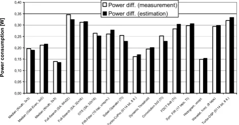
Obviously, the part of the total power consumption according to the clock system is a constant offset for each algorithm which is performed on the processor. Therefore, for a fair comparison differential power consumption values (neglecting the clock system) should also be regarded. The comparison depicted in Figure 9 yields a maxi-mum error of 10%. It should be noticed that according to the program to be performed on the processor the differential power consumption varies by more than 200 mW. This dynamics is much larger than the maximum estimation error of about ten to twenty mW.
0,00 0,05 0,10 0,15 0,20 0,25 0,30 0,35 0,40
Media n (Kn
uth, 3 x3)
Medi an (O
dd-E ven,
3x3)
Medi an (K
nuth, 5x3)
Full-S earch
(SA: 64x
32)
Full-S earc
h (SA: 32x16
)
OTS ( SA: 3
2x16)
FI R-Filter
(1 5-tap,
unsy m.)
Sobel -Ope
rato r (TI)
Turb o-CoP
ro (5 114
bit, 8 It.)
Dyna mic T
hresh old
Conv olution
3x3 (TI)
FDCT 8x8
(TI)
Sym . FIR (1
7 taps, TI)
Histog ram,
unop t.
Wave let, h
orz. ( 8 taps)
Tur bo-DSP (
5114 bit, 8
It.)
P
o
w
e
r co
ns
um
pt
io
n
[W
]
Power diff. (measurement) Power diff. (estimation)
Figure 9. FLPA power estimation results and measurements for the TMS320C6416 (differential power consumption)
The FLPA approach has also been applied to the C6711 processor which is a floating point processor pro-viding no further co-processors. The C6711 FLPA model comprises seven model functions. Compared to the set of algorithms which have been taken as benchmarking set for the C6416 the benchmarking set for the C6711 also included dedicated floating point applications like floating point matrix multiplications. The maximum power consumption of the C6711 within the experiments amounted to 1.1 W and the dynamics concerning the power consumption of the different algorithms amounted to 350 mW. A comparison between the FLPA power estimation and physical measurements yields a maximum error of less than 5% for the absolute power consumption and less than 10% (40 mW) for the differential power consumption (see Figure 10). Again this comparison proves that the FLPA methodology provides sufficient accuracy for a power estimation in an early stage of the design flow.
Fig. 8. FLPA power estimation results and measurements for the
TMS320C6416 (absolute power consumption).
The power consumption of the processing unit has three significant parameters:
– the degree of parallelismα(percentage of parallel work-ing functional units),
– the number of executed instructions, – the type of input data.
The scenarios belonging to the processing unit vary these pa-rameters separately.
In Fig. 6 the current drawn by the processing unit is de-picted over the degree of parallelism. The applied test sce-nario includes a loop where within each loop iteration 1000 instructions are executed. The dotted line of Fig. 6 represents the worst-case power consumption of the processing unit, in which complex instructions (e.g. multiplications) with the maximum word length of the input data (32 bit) are exe-cuted. In contrast to that, the dashed line represents the best-case power consumption with simple instructions (e.g. addi-tions) and a small word length of the input data (8 bit). The arithmetic function belonging to the straight line (typical-case: instruction mix, medium word length of the input data (16 bit)) is chosen as model function for the FLPA model of the TMS320C6416 processing unit and modeled by
Pprocessing unit=(1.02·10−1·α+2.46·10−2)·Vcore
=IDD,processing unit·Vcore. (2)
Table 1. Model functions of the functional blocks of the TMS320C6416 and belonging list of parameters.
functional block block specific power consumption function clock system Pclock system = (a·F+b) ·VCore
fetch unit Pfetch unit = (c·α2+d·α+e) ·F· (1-PSR) ·VCore processing unit Pproc. unit = (f·α+g) ·F· (1-PSR) ·VCore internal memory Pinternal memory = (h·β+i·γ)·F· (1-PSR) ·VCore level-1 cache Plevel-1 cache = (j·δ+k·ε)·F· (1-PSR) ·VCore EDMA/QDMA PEDMA/QDMA = (m·ζ)·F· (1-PSR) ·VCore co-processors (Turbo,
Viterbi) Pcopro = (n· η +p· θ)·F· (1-PSR) ·VCore
parameter description parameter description
α parallelism degree θ Turbo co-processor activity rate
β memory access rate (read) η Viterbi co-processor activity rate
γ memory access rate (write) VCore Core Voltage of the processor
δ L1P cache miss rate F clock frequency ε L1D cache miss rate PSR pipeline stall rate ζ EDMA activity rate
a,b,c,d,e,f, g,h,i,j,k,m, n,p
coefficients for polynomials
Here,VCore denotes the core-voltage of the processing unit
andαthe achieved degree of parallelism. The error of the estimated power consumption for algorithms with either tremely complex or extremely simple instructions will be ex-amined in the next section.
The architecture of the fetch unit of the TMS320C6416 has the task to control the flow of VLIW instruction words to the DSP core and to dispatch the atomic instructions to the functional units. Though the architecture of the fetch unit of the TMS320C6416 is not known in detail it is possible to model this functional block. In a test scenario the only parameter having a strong impact on the power consumption of the fetch unit, the parallelism degreeα, is varied and some working points are measured. Figure 7 depicts the current consumption drawn by the fetch unit.
According to the measured working points a polynomial function (here, a quadratic function) can be found which de-scribes the power consumption of the fetch unit
Pfetch unit=
(−5.67·10−2·α2+1.14·10−1·α+3.02·10−2)·Vcore
=IDD,fetch unit·Vcore. (3)
All the other FLPA blocks depicted in Fig. 5 can be mod-eled similarly. The complete FLPA power model of the TMS320C6416 including the complete list of required pa-rameters is shown in Table 1.
4 Results
M. Schneider et al.: Power estimation on functional level for programmable processors 219 4 Results
For the evaluation of the FLPA methodology the power consumption was measured as well as estimated for a variety of digital signal processing algorithms. The comparison of estimated and measured values shows a maximum error of 3%, as can be seen in Figure 8. All algorithms which are marked with (TI) have been taken from the TI code library in order to apply the methodology also for DSP code which was optimized by the processor manufacturer himself.
0,0 0,1 0,2 0,3 0,4 0,5 0,6 0,7 0,8 0,9
Med ian (K
nuth, 3x3
)
Median (Odd
-Eve n, 3x
3)
Medi an (K
nuth , 5x3
)
Full-Se arch (
SA: 64 x32)
Full-S earc
h (SA : 32x
16)
OTS ( SA: 32
x16)
FIR-F ilter (1
5-tap, unsym
.)
Sobe l-Ope
rator (TI)
Tur bo-CoPr
o (51 14 bi
t, 8 It .)
Dyna mic T
hres hold
Convo lution
3x3 (T I)
FDCT 8x8 (T
I)
Sym . FIR
(17 ta ps, T
I)
Histo gram
, uno pt.
Wave let, ho
rz. (8 t aps)
Turbo -DSP
(511 4 bit,
8 It.)
P
o
w
e
r consu
m
pt
ion [
W
]
Power abs. (measurement) Power abs. (estimation)
Figure 8. FLPA power estimation results and measurements for the TMS320C6416 (absolute power consumption)
Obviously, the part of the total power consumption according to the clock system is a constant offset for each algorithm which is performed on the processor. Therefore, for a fair comparison differential power consumption values (neglecting the clock system) should also be regarded. The comparison depicted in Figure 9 yields a maxi-mum error of 10%. It should be noticed that according to the program to be performed on the processor the differential power consumption varies by more than 200 mW. This dynamics is much larger than the maximum estimation error of about ten to twenty mW.
0,00 0,05 0,10 0,15 0,20 0,25 0,30 0,35 0,40
Media n (Kn
uth, 3 x3)
Median (Odd
-Even, 3x3)
Medi an (K
nuth, 5x3)
Full-S earch
(SA: 64x
32)
Full-S earc
h (SA: 32x16
)
OTS ( SA: 3
2x16)
FI R-Filter
(1 5-tap, u
nsym .)
Sobel -Ope
rato r (TI)
Turb o-CoP
ro (5 114
bit, 8 It.)
Dyna mic T
hresh old
Conv olution
3x3 (T I)
FDCT 8x8
(TI)
Sym . FIR (1
7 tap s, T
I)
Histog ram,
unop t.
Wave let, h
orz. ( 8 taps)
Tur bo-DSP (
5114 bit, 8
It.)
P
o
w
e
r co
ns
um
pt
io
n
[W
]
Power diff. (measurement) Power diff. (estimation)
Figure 9. FLPA power estimation results and measurements for the TMS320C6416 (differential power consumption)
The FLPA approach has also been applied to the C6711 processor which is a floating point processor pro-viding no further co-processors. The C6711 FLPA model comprises seven model functions. Compared to the set of algorithms which have been taken as benchmarking set for the C6416 the benchmarking set for the C6711 also included dedicated floating point applications like floating point matrix multiplications. The maximum power consumption of the C6711 within the experiments amounted to 1.1 W and the dynamics concerning the power consumption of the different algorithms amounted to 350 mW. A comparison between the FLPA power estimation and physical measurements yields a maximum error of less than 5% for the absolute power consumption and less than 10% (40 mW) for the differential power consumption (see Figure 10). Again this comparison proves that the FLPA methodology provides sufficient accuracy for a power estimation in an early stage of the design flow.
Fig. 9. FLPA power estimation results and measurements for the
TMS320C6416 (differential power consumption).
with (TI) have been taken from the TI code library in order to apply the methodology also for DSP code which was op-timized by the processor manufacturer himself.
Obviously, the part of the total power consumption accord-ing to the clock system is a constant offset for each algorithm which is performed on the processor. Therefore, for a fair comparison differential power consumption values (without the clock system) should also be regarded. The comparison depicted in Fig. 9 yields a maximum error of 10%. It should be noticed that according to the program to be performed on the processor the differential power consumption varies by more than 200 mW. This dynamics is much larger than the maximum estimation error of about ten to twenty mW.
The FLPA approach has also been applied to the C6711 processor which is a floating point processor providing no further co-processors. The C6711 FLPA model comprises seven model functions. Compared to the set of algorithms which have been taken as benchmarking set for the C6416 the benchmarking set for the C6711 also included dedicated floating point applications like floating point matrix multi-plications. The maximum power consumption of the C6711 within the experiments amounted to 1.1 W and the dynam-ics concerning the power consumption of the different al-gorithms amounted to 350 mW. A comparison between the FLPA power estimation and physical measurements yields a maximum error of less than 5% for the absolute power consumption and less than 10% (40 mW) for the differen-tial power consumption (see Fig. 10). Again this comparison proves that the FLPA methodology provides sufficient accu-racy for a power estimation in an early stage of the design flow.
5 Conclusion
Different approaches for power estimation for programmable processors have been described and evaluated concerning their capability to be applied to modern digital signal proces-sor (DSP) architectures like e.g. Very Long Instruction Word (VLIW)-architectures. The concept of so-called Functional-Level Power Analysis (FLPA) has been extended and refined and the belonging separation of the processor architecture
0,00 0,10 0,20 0,30 0,40 0,50 0,60 0,70
2D-FIR-Filter (3x3, TI ref. code)
Sobel (TI ref. code)
Median (3x3, TI ref. code)
Median (Odd-Even-Transp.,
3x3)
Median (Odd-Even-Transp.,
3x1)
Endian-Swap (32 Bit)
Matrix mul. Float (16x16)
Powe
r co
nsum
pt
io
n
[W
] Power diff. (measurement)
Power diff. (estimation)
Figure 10. FLPA power estimation results and measurements for the TMS320C6711 (differential power consumption)
5 Conclusion
Different approaches for power estimation for programmable processors have been described and evaluated concerning their capability to be applied to modern digital signal processor (DSP) architectures like e.g. Very Long Instruction Word (VLIW) -architectures. The concept of so-called Functional-Level Power Analysis (FLPA) has been extended and refined and the belonging separation of the processor architecture into functional blocks has been shown. The power consumption of these blocks has been described in terms of parameterized arithmetic model functions. A parser which allows to analyze automatically the assembler codes has been imple-mented. This parser yields the input parameters of the arithmetic functions like e.g. the achieved degree of parallelism or the kind and number of memory accesses. A demonstration and evaluation of this approach has been performed applying the DSPs TMS320C6416 and TMS320C6711 and a variety of basic algorithms of digi-tal signal processing. Resulting estimation values for the inspected algorithms are compared to measured values. A resulting maximum estimation error of 3% for the absolute power consumption and 10% for the differential power consumption is achieved. The application of this methodology allows to evaluate efficiently different parameter settings of a programmable processor like different coding styles, compiler settings, algorithmic alternatives etc. concerning the resulting power consumption. Therefore, it is a valuable methodology for a system designer to explore the design space of programmable processors concerning the power aspect.
References
Brooks, D.; Tiwari, V.; Martonosi, M.: "Wattch: A Framework for Architectural-Level Power Analysis and Optimizations", Proceedings of the ISCA, 2000, pp. 83-94
Marwedel, P.: "Fast, predictable and low-energy memory references through memory-architecture aware compilation", Proceedings of the DSP Design Workshop 2003, Dresden, 25.11.2003
Qu, G.; Kawabe, N.; Usami, K.; Potkonjak, M.: "Function Level Power Estimation Methodology for Microprocessors", Proc. of the Design Automation Conference 2000, pp. 810-813
Senn, E.; Julien, N.; Laurent, J.; Martin, E.: "Power Consumption Estimation of a C Program for Data-Intensive Applications", Proc. of the PATMOS Conference 2002, pp. 332-341
Tiwari, V.; Malik, S.; Wolfe, A.: "Instruction Level Power Analysis and Optimization of Software", Journal of VLSI Signal Processing 1996, pp. 1-18
TMS320C6416 Fixed Point Digital Signal Processor, Texas Instruments, Sep. 2001, SPRS164C TMS320C6711 datasheets, website, http://www.ti.com
Fig. 10. FLPA power estimation results and measurements for the
TMS320C6711 (differential power consumption).
into functional blocks has been shown. The power consump-tion of these blocks has been described in terms of parame-terized arithmetic model functions. A parser which allows to analyze automatically the assembler codes has been imple-mented. This parser yields the input parameters of the arith-metic functions like e.g. the achieved degree of parallelism or the kind and number of memory accesses. A demonstration and evaluation of this approach has been performed applying the DSPs TMS320C6416 and TMS320C6711 and a variety of basic algorithms of digital signal processing. Resulting estimation values for the inspected algorithms are compared to measured values. A resulting maximum estimation error of 3% for the absolute power consumption and 10% for the differential power consumption is achieved. The application of this methodology allows to evaluate efficiently different parameter settings of a programmable processor like differ-ent coding styles, compiler settings, algorithmic alternatives etc. concerning the resulting power consumption. Therefore, it is a valuable methodology for a system designer to explore the design space of programmable processors concerning the power aspect.
References
Brooks, D., Tiwari, V., and Martonosi, M.: Wattch: A Framework for Architectural-Level Power Analysis and Optimizations, Pro-ceedings of the ISCA, 83–94, 2000.
Marwedel, P.: Fast, predictable and low-energy memory references through memory-architecture aware compilation, Proceedings of the DSP Design Workshop 2003, Dresden, 2003.
Qu, G., Kawabe, N., Usami, K., and Potkonjak, M.: Function Level Power Estimation Methodology for Microprocessors, Proc. of the Design Automation Conference 2000, 810–813, 2000. Senn, E., Julien, N., Laurent, J., and Martin, E.: Power
Consump-tion EstimaConsump-tion of a C Program for Data-Intensive ApplicaConsump-tions, Proc. of the PATMOS Conference 2002, 332–341, 2000. Tiwari, V., Malik, S., and Wolfe, A.: Instruction Level Power
Anal-ysis and Optimization of Software, Journal of VLSI Signal Pro-cessing, 1–18, 1996.
TMS320C6416: Fixed Point Digital Signal Processor, Texas Instru-ments, SPRS164C, 2001.