www.advmattechnol.de
Parallel Process 3D Metal Microprinting
Yen-Po Lin, Yong Zhang, and Min-Feng Yu*
DOI: 10.1002/admt.201800393
and even nanoscale resolution, and also with process compatibility to existing microfabrication processes to enable com-pact microsystem integration, there seems to be no obvious solution if metal powder fusion–based 3D printing method would be relied upon.
An alternative method to make high-quality metal components with the additive manufacturing concept is through electro-deposition. Electrodeposition-based elec-troforming[22] has been applied in industry
for metal forming to produce precision and high-quality 3D metal structures for over a century. The more advanced LIGA (a German acronym that stands for lithography, electroforming, and molding) process[23] is, in essence, also an
electro-forming one, which relies on X-ray based lithography to produce the precision mold having microscale resolution and high aspect ratio features for electroforming. While such processes can produce 3D metal components with microscale and even nanoscale resolution, they are not process-compatible to existing photolithography-based microfabrication processes for potential cross-length scale integration with, especially, microelectronics. In the meantime, electrodeposition of metal has been widely used in photolithog-raphy-based microfabrication and in surface micromachining-based micro-electro-mechanical systems (MEMS) fabrication;[24]
however, the 3D structuring, the aspect ratio, and the height of thus fabricated metal structures are quite limited. There are also recent attempts to “print” 3D metal microstructures with a nozzle-based approach with or without involving electrodepo-sition; one involves exploiting the low melting temperature of Ga to print 3D Ga structures,[25] and the others implement the
nozzle-confined electrodeposition[5,9,26,27] to produce 3D metal
structures. Aside from issues related to making structures that can meet quality requirement for electronics industry applica-tion, they are still limited to serial process fabrication. To have the capability to “print” truly high quality 3D metal freeform structures and structure arrays in a parallel process with sub-micrometer feature resolution and unrestricted z-dimension access can provide the ultimate engineering solution to com-pact 3D microsystem integration and packaging where such metal structures can serve as both structural components and electrical interconnections. It can thus open up new opportu-nities for significant packaging volume miniaturization with increased functionality for critical applications especially in medical implant and imbedded sensor system.
Herein, we develop a 3D metal microprinting technology that realizes the 3D printing of high mechanical and elec-trical quality metal wire structures with microscale and even
3D printing, as an additive manufacturing technology, enables agile and free-form fabrication of complex 3D structures relevant to industrial applica-tion. However, the 3D structure forming mechanisms in existing 3D printing technologies hinder and even prevent the manufacturing of ultra-precision 3D metal parts, let alone parallel process manufacturing. A generic 3D elec-trochemical microprinting technology that allowed the “printing” of ultrahigh density, ultrahigh aspect ratio, and electronics quality 3D copper structures with microscale and even nanoscale precision in an ambient environment is developed here. Further on, the feedback-controlled and self-regulated “printing” mechanism was demonstrated to be capable of realizing parallel process 3D “printing” of an array of identical copper microstructures simul-taneously, promising large-scale 3D printing–based production of precision metal structures for broad applications in 3D integration of electronics and sensor systems.
Dr. Y.-P. Lin, Dr. Y. Zhang, Prof. M.-F. Yu School of Aerospace Engineering Georgia Institute of Technology
270 Ferst Drive, NW, Atlanta, GA 30332, USA E-mail: [email protected]
The ORCID identification number(s) for the author(s) of this article can be found under https://doi.org/10.1002/admt.201800393. 3D Printing
Additive manufacturing of metal components remains one of the most impactful area for research and development.[1–12] To
be relevant to industrial applications, such metal components must meet some stringent performance requirements through rigorous mechanical, electrical, thermal, and environmental testing.[13–18] Among existing additive manufacturing
technolo-gies, laser or electron beam sintering (and melting) based 3D metal printing technologies are the economically most viable ones that are capable of fabricating metal components to meet such quality requirements, and have been adopted by industry to produce special automotive, aerospace, and medical metal components.[19–21] High energy–focused laser or electron beam
is used to selectively fuse a bed of metal powders of uniform diameter in the range of 10–30 µm layer-by-layer to build up the desired macroscopic 3D metal structures. However, limited by the thermal physics involved in the intense interaction between high energy beam and material,[15] and the use of metal
pow-ders of tens of micrometers in diameter, the as-produced part has typically a surface roughness in the low-ten micrometer range,[21] and needs to be mechanically polished before being
useful. While current 3D metal printing technologies provide economical alternatives for making macroscopically complex 3D parts, toward precision 3D metal printing with microscale
nanoscale resolution at room temperature. We demonstrate the fabrication of ultra-high density and ultraultra-high aspect ratio 3D metal micro- and nanostructures through a feedback-controlled, electrodeposition-based printing process. Furthermore, a self-regulated electrodeposition mechanism is exploited to realize the parallel process 3D printing by simultaneously printing multiple identical 3D metal microstructures with the use of a nozzle array.
The principle of the 3D metal micro-printing is schematically shown in Figure 1. Similar to the conventional extrusion-based 3D printing of polymer, a nozzle (a glass pipette produced with a commercially avail-able pipette puller) controlled by a piezo-electric stage–based precision positioning system with 1 nm resolution is used to sequentially lay down a thin layer of mate-rial (or termed a voxel in 3D printing) at each designated site on a flat and conduc-tive substrate with good water wettability to build up a 3D structure. In this develop-ment, electrodeposition was used to produce the metal voxels with the use of a nozzle (or a nozzle array) filled with the needed electrolyte, and the meniscus-confined elec-trodeposition principle[5] was exploited to
control the quality of the deposited metal voxels as shown at the third and fourth steps in the schematic. The 3D metal micro-printing method implemented a feedback mechanism to detect the surface of con-tact by detecting the initiated ionic current at the moment when the meniscus at the nozzle opening makes contact with metal surface (at the second step) to acquire the
x–y–z coordinates of each local site in the
evolving fabrication process, and used that information to determine the amount of deposition needed in the subsequent steps to realize a leveled build-up across all sites of deposition. In addition, incorporating the meniscus-confined electrodeposition principle allowed the precise control of the dimensions of the metal voxels deposited at every site. In this study, the diameter of each deposited metal segment was varied from 200 nm to 25 µm, and the thickness from 100 nm to 2 µm. Ultrahigh density and ultrahigh aspect ratio metal microstruc-ture arrays were readily fabricated, as shown in Figure 1b,c. The layer-by-layer nature
of the printed metal structures was clearly seen in the struc-tures, which in return, manifests also the successful develop-ment of meniscus formation in each and every print. With nanopositioning motion control, there is practically no limit on how close the structures can be fabricated in neighboring
to each other, thus achieving ultrahigh array density for high aspect ratio microstructures beyond the existing capabilities of MEMS surface micromachining, LIGA, or direct-write fab-rication. We extended this 3D microprinting to nanoprinting with the simple use of a pipette having a nozzle diameter Figure 1. 3D metal microprinting. a) Schematic showing the steps involved in the 3D metal microprinting. The overall process is similar to the conventional extrusion type of 3D printing, except that electrochemical deposition by a microscale nozzle filled with electrolyte is used to sequentially deposit metal layers, and meniscus stability governed self-regulated metal layer growth is exploited to control the leveled build-up of the 3D metal structure. b) An ultrahigh array density solid Cu wire array of 25 µm in height and wall-to-wall spacing of only ≈350 nm produced with 3D microprinting. The wire diameter is ≈2 µm. The printing layer thickness is 1 µm. The scale bar is 4 µm. c) Magnified view of the top of the array in (b) showing the lev-eled and homogeneous surface finish. The scale bar is 2 µm. d) SEM image showing four Cu wires of ≈300 nm in diameter and 20 µm in height printed with layers of ≈100 nm in thickness produced with 3D metal nanoprinting. The scale bar is 2 µm.
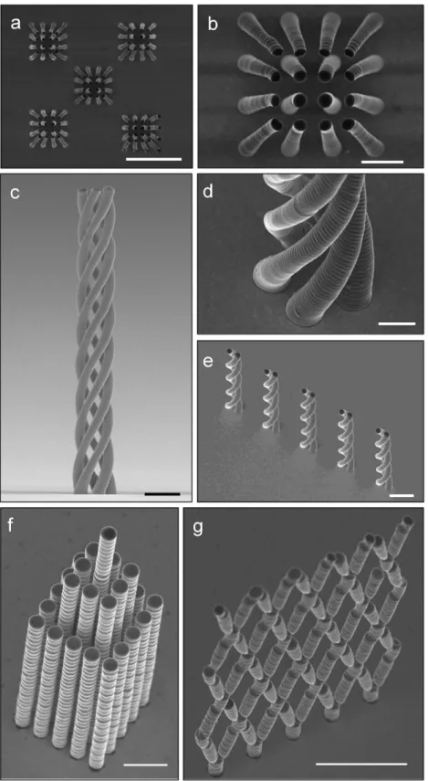
Figure 2. Complex metal structures and structure arrays fabricated with 3D metal microprinting. a) An array of Cu wires in a truncated square pyramid configuration to reduce the electrode array spacing from 5 to 2.5 µm. The array height is ≈10 µm. The scale bar is 25 µm. b) Magnified view of the top of the array in (a) showing the reducing array spacing and the leveled electrode termination. The scale bar is 5 µm. c) SEM image showing a Cu quintuple helix structure fabricated with the 3D microprinting. The height of helix is ≈44 µm and the wire diameter is ≈2 µm. The scale bar is 5 µm. d) Magnified view of the base showing the layered construction of the helix. The scale bar is 2 µm. e) SEM image showing an array of Cu double helixes of 28.5 µm in height printed with layers of 200 nm in thickness. The scale bar is 5 µm. f) SEM image showing a high array density Cu wires with varying heights. The scale bar is 5 µm. g) SEM image showing an interconnected truss structure of solid Cu wires. The scale bar is 10 µm.
of ≈250 nm as shown in Figure 1d. High aspect ratio metal wires of ≈200 nm in diameter were printed with layered depo-sition of metal of 100 nm in thickness in each print. As the piezoelectric positioning system has a positioning resolution of 1 nm, the printing resolution is very high as well, close to 1 nm, excluding the existence of any thermal drift in the system due to environment condition variations. Taking into practical consideration of the stability of the mechanical system and the stability of the meniscus formation, we expect that this printing process can be further extended to print sub-100 nm diameter structures.
Taking advantage of the digitized construction principle of 3D printing, various metal microstructures with complex 3D geometry were also fabricated, as shown in Figure 2a–g. This ability to print precise 3D metal structures and structure arrays with micrometer and even nanometer resolution without involving high temperature (as in focused laser melting–based printing) and other restricting conditions (such as the high vacuum required in focused electron beam melting–based printing) provides the ultimate design flexibility to integrate 3D functionalities into microchips.
The rate of electrodeposition for metal is inherently slow compared to the extrusion of polymer or the fusion of metal particles in other 3D printing methods. However, when higher feature resolution is required, the rate of deposition in such existing 3D printing methods slows down significantly as well,[14] not to mention that such extrusion-based or metal
particle fusion–based 3D printing methods are not capable of achieving submicrometer fabrication resolution, as limited by the corresponding physical mechanisms. We explore means to improve the efficiency of our 3D metal microprinting, one through the understanding of the layer-by-layer electrodeposi-tion process and the other by the development of a parallel pro-cess microprinting technology.
Due to the existence of a liquid/air interface in our meniscus-confined electrodeposition, and thus the continuous evapora-tion of water off the microscale meniscus, as we explained pre-viously in ref. [5], the rate of metal deposition is intrinsically higher than the corresponding electroplating process typically performed in an electrolyte bath. The “on-and-off” nature of the printing process promotes this evaporation further, and allows the first, the quick replenish of the metal ions in the meniscus through diffusion and the second, the conditioning of the elec-trolyte in the meniscus to higher concentration (than the bulk concentration) through water evaporation, during the “off” stage. Both are favorable conditions for realizing higher elec-trodeposition rate for depositing the metal layer in the subse-quent “on” stage. The solid line in Figure 3 shows the acquired variation of electrodeposition current in time during the micro-printing process for four layers of Cu. For the study, a pipette having a nozzle diameter of ≈5 µm filled with 0.5 m CuSO4
aqueous solution was used for the microprinting and the elec-trodeposition potential was set to 0.2 V relative to the Au-coated substrate. The acquired ionic current variation resembles that of a typical pulsed electrodeposition. The current variation fol-lows the microprinting process described in the schematic of Figure 1. A narrow peak preceding a wide peak in each printing period indicates the detection of the metal surface through the formation of a liquid contact with the metal surface under the applied electrical potential (the second step in Figure 1). The current variation during the electrodeposition of the metal layer (the fourth step in Figure 1) is described by the wide peak. At the completion of depositing the first Cu layer to the desired thickness (≈300 nm), the applied electrical potential is set to zero, and the nozzle is lifted up to break off the meniscus and driven to the next site to deposit the next layer repeating the same process. The rate of deposition within the “on” stage of the microprinting process was calculated by integrating the Figure 3. Ionic current response in the 3D microprinting process. a) Plot showing the ionic current variation in time during the electrodeposition of four metal layers (solid curve) acquired from the printing of a Cu wire with the use of nozzle having a diameter of ≈5 µm. The current variation follows the microprinting stages described in Figure 1. The narrow peak indicates the detection stage for locating the exact x–y–z coordinates of the starting surface for printing, and the wide peak indicates the electrodeposition stage to deposit a metal layer of a designated thickness, in each printing period. The ionic current variation in time (the dotted line) acquired during the continuous electrodeposition of a Cu wire of ≈5 µm in diameter realized within the stability limit of the meniscus by synchronizing the nozzle withdrawal speed with the (height growth) rate of the wire (at 170 nm s−1) was included
for comparison. b) SEM image showing the surface finish of the continuously electrodeposited Cu wire. c) SEM image showing the microprinted Cu wire and the layered presence. Both scale bars are 3 µm.
current curve over time, and by knowing the diameter of depos-ited wire. It was determined to be 215 nm s−1, which matched
well with that calculated through measuring the layer thick-ness in a scanning electron microscope (SEM). In comparison, the same nozzle was used to continuously grow a Cu wire at a nozzle withdrawal speed synchronized with the height growth rate of the Cu wire without going through the “on-and-off” printing process, and the acquired variation of current in time was included as the dotted line in Figure 3. The rate of deposi-tion was determined to be ≈170 nm s−1, 20% smaller than the
rate in the printing process. The surface quality of the printed metal is comparable to the continuously grown one as shown in the figure. Even higher quality surface finish is attainable with the printing of even thinner metal layers. The mechanical quality of the printed metal was also characterized. Its elastic modulus was measured to be 116.4 ± 4.0 GPa in a cantilever bending test with Hysitron Nanoindenter, matched well with
the value for bulk copper, generally around 120 GPa. This was expected as the sequential metal layers were fabricated through electro-deposition and were bonded together with atomic quality interfaces.
Certainly, the overall rate of fabrication should also take into account the “off” time in each period of layer deposition. Consid-ering the printing of a wire of a fixed height by depositing layers of thickness of h each, the rate of fabrication is then h/(ton + toff),
where ton and toff are the time durations set
for the electrodeposition stage and the rest for printing each layer, respectively. ton= h/v,
where v is the rate of electrodeposition or the withdrawal speed of the nozzle that can sus-tain the electrodeposition of metal to a cersus-tain thickness before the meniscus breaks. toff is
the time duration mostly needed for trans-lating the nozzle to a new neighboring site and is typically fixed. The rate of fabrication is then h/(h/v + toff). As toff is typically larger
than ton, it is understood that the highest
rate of fabrication is realized by maximizing the printed thickness of each layer with the highest withdrawal speed of the nozzle. Note that this v is above the speed parameter window of stability for maintaining the stable meniscus formation during the whole syn-chronized and sustained electrodeposition process, so only a thin layer of metal can be deposited before the meniscus is stretched to break. The higher this nozzle withdrawal speed goes, the thinner is the deposited metal layer. The optimal rate of fabrication is thus simply determined by the needed layer thickness resolution and the highest nozzle withdrawal speed capable of just producing that desired layer thickness.
The incorporation of the self-regulated growth mechanism in the meniscus-confined electrodeposition enabled also the realiza-tion of multinozzle-based parallel process 3D printing, which had yet been demonstrated in existing 3D printing systems. One of the key issues to be resolved is how to maintain the lev-eled build-up of materials under every nozzle across the whole nozzle array. This includes actually two sub-issues, one is the leveled build-up of materials under individual nozzle since each nozzle is responsible for printing a 3D structure, and the other is the leveled build-up of materials under every nozzle.
The leveled build-up of materials under individual nozzle in this 3D metal microprinting method is realized, as we described previ-ously, by detecting the surface of contact to acquire the x–y–z coor-dinates of the local site for printing, and using that information as the feedback to determine the amount of deposition needed in the subsequent steps. As shown in the printed structures in Figures 1 and 2 with the use of a single nozzle, no accumulated height vari-ation was noticed between the wire structure elements after many tens of layers and even hundreds of layers of printing.
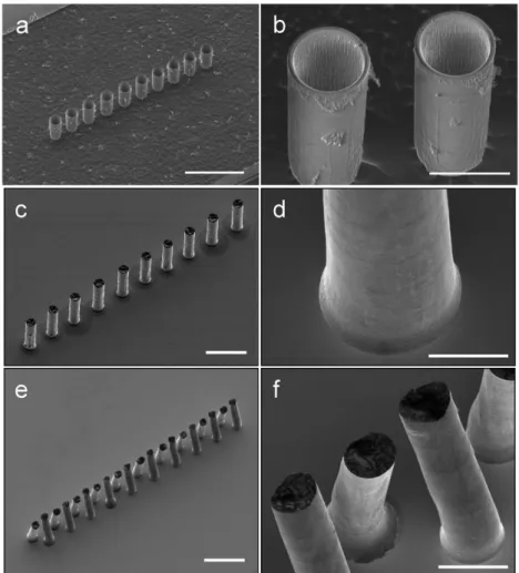
Figure 4. Parallel process 3D microprinting of metal structures. a) SEM image showing the microfabricated nozzle array for the parallel process microprinting. The scale bar is 150 µm. b) Magnified view of the nozzles in the nozzle array. The scale bar is 30 µm. c) SEM image showing an array of Cu wires of 20 µm in diameter and 80 µm in height simultaneously printed with the nozzle array–based microprinting method. The metal layer thickness is 500 nm in each print. The scale bar is 100 µm. d) Magnified view showing the layered texture in the printed wire. The scale bar is 10 µm. e) SEM image showing an array of tilted wire-pairs of 100 µm in height printed with the nozzle array–based microprinting method. Each nozzle is responsible to print one pair of such tiled wires. The scale bar is 100 µm. f) Magnified view showing the surface finish of the printed wires. The metal layer thickness is 500 nm. The scale bar is 20 µm.
The leveled build-up of materials under every nozzle is only possible with the involvement of the self-regulated growth mechanism[5] in the meniscus-confined electrodeposition. The
thermodynamic stability (or the deformability) of the liquid meniscus formed between the nozzle end opening and the growth front of the metal wire dictates a self-regulated elec-trodeposition growth of the wire. In the nozzle array–based printing, the variation in nozzle dimension and the mis-alignment of the nozzle array with the substrate practically exist. However, within the thermodynamic stability limit of the meniscus, meniscus formation can be realized between every nozzle opening and the corresponding growth front of the metal wire, albeit the stable shape of the meniscus varies slightly from one nozzle to another. For example, at a place with more separation between nozzle opening and metal wire, the meniscus is stretched more, which, during the meniscus-con-fined electrodeposition, results in the deposition of a metal wire segment of less diameter but with a higher (height growth) rate. This effectively levels out the initial unevenness of the growth fronts of all wires under all nozzles. The same leveling effect exists due to the slight variation of nozzle diameters across the nozzle array. This leveled build-up of materials, in return, makes the feedback control possible, as the development of meniscus under one nozzle opening guarantees the develop-ment of menisci under all nozzle openings during the printing process, as long as the nozzles are uniform in size across the whole array and coplanar, and the nozzle array is coplanarly prealigned with the flat substrate with sufficient accuracy.
Figure 4 shows the parallel process printing of metal
struc-tures with the use of a 1 by 10 nozzle array. The nozzle array was fabricated with the standard micromachining method of a silicon wafer. The nominal nozzle inner diameter is 20 µm. 3D microprinting process was applied to produce 10 identical metal microstructures and microstructure pairs simultaneously with each microstructure being fabricated according to the designed 3D configuration. Layered formation of such micro-structures was only visible under high magnification, again manifesting their high structural quality. One of the immediate outcomes of applying this parallel process 3D microprinting is that the array density of the fabricated metal structures can significantly exceed the array density of the microfabricated nozzle array used for 3D microprinting, in addition to prior described benefits.
With a properly designed and fabricated nozzle array (with larger inter-nozzle spacing), an array of more complicated 3D metal microstructures as those presented in Figure 2 can be produced with this parallel process printing process to significantly multiply the production. A larger nozzle array may also be microfabricated and be used to efficiently produce a larger array of potentially ultrahigh density and ultrahigh aspect ratio three dimensionally designed micro-structures that has so far been beyond the reach of existing microfabrication capabilities. Furthermore, other 3D micro-/ nanostructure forming mechanisms such as e-jet, electrohy-drodynamic, and even evaporation drying–based local deposi-tions[4,28,29] can be potentially integrated into such a nozzle
array–based parallel manufacturing process to further expand the material base for the scaled-up 3D fabrication of micro- and nanostructures.
Experimental Section
Microfabrication of Nozzle Array: Standard micromachining fabrication
processes were applied to fabricate the nozzle array. A double-side polished Si wafer of 480 µm in thickness was first coated with a Si3N4
film of 100 nm in thickness onto the front side. The wafer was then photolithographically patterned and etched from the back side with deep reactive ion etching (DRIE) to form a cavity as the electrolyte reservoir. The Si3N4 side of the wafer was then patterned to define the circular nozzle
shapes and reactive ion etching was used to etch away the exposed circular nitride layer. DRIE was then used to etch through the Si membrane to form the nozzle channels. The Si surfaces not covered by Si3N4 (including
the inner surfaces of the channels) were then thermally oxidized to form 1 µm thick SiO2 layers. The remaining Si3N4 was etched off by reactive ion
etching, and finally DRIE was used to etch down silicon from the front side to expose SiO2 shells that would serve as the protruding array nozzles for
the parallel process microprinting electrodeposition.
Mechanical Measurement: Elastic property of three microprinted
Cu wires was measured through a cantilever bending test by laterally deflecting the free end of the Cu wires in a Hysitron Nanoindenter with a flat-ended tip. The Cu wires had a diameter of ≈21 µm and a length of ≈146 µm. The point of application for the bending test was set to be 20 µm from the free end. Multiple tests were conducted on each of the three Cu wires and the force–deflection curves were acquired. A standard cantilever stiffness model was then applied to deduce the Young’s modulus of the Cu wires.
Acknowledgements
The work was supported by National Science Foundation under grant CMMI1516097 and by Georgia Institute of Technology. The work was performed in part at the Georgia Tech Institute for Electronics and Nanotechnology, a member of the National Nanotechnology Coordinated Infrastructure (NNCI), which was supported by the National Science Foundation (ECCS-1542174).
Conflict of Interest
The authors declare no conflict of interest.
Keywords
electrodeposition, metal 3D printing, parallel process manufacturing
Received: August 27, 2018 Revised: October 17, 2018 Published online: November 12, 2018
[1] W. Gao, Y. Zhang, D. Ramanujan, K. Ramani, Y. Chen, C. B. Williams, C. C. Wang, Y. C. Shin, S. Zhang, P. D. Zavattieri,
Comput.-Aided Des. 2015, 69, 65.
[2] M. A. Skylar-Scott, S. Gunasekaran, J. A. Lewis, Proc. Natl. Acad. Sci.
U. S. A. 2016, 201525131.
[3] J. A. Lewis, J. E. Smay, J. Stuecker, J. Cesarano, J. Am. Ceram. Soc. 2006, 89, 3599.
[4] B. Y. Ahn, E. B. Duoss, M. J. Motala, X. Guo, S.-I. Park, Y. Xiong, J. Yoon, R. G. Nuzzo, J. A. Rogers, J. A. Lewis, Science 2009, 323, 1590.
[5] J. Hu, M.-F. Yu, Science 2010, 329, 313.
[6] T. A. Schaedler, A. J. Jacobsen, A. Torrents, A. E. Sorensen, J. Lian, J. R. Greer, L. Valdevit, W. B. Carter, Science 2011, 334, 962.
[7] Z. C. Eckel, C. Zhou, J. H. Martin, A. J. Jacobsen, W. B. Carter, T. A. Schaedler, Science 2016, 351, 58.
[8] R. D. Farahani, K. Chizari, D. Therriault, Nanoscale 2014, 6, 10470.
[9] L. Hirt, S. Ihle, Z. Pan, L. Dorwling-Carter, A. Reiser, J. M. Wheeler, R. Spolenak, J. Vörös, T. Zambelli, Adv. Mater. 2016, 28, 2311.
[10] P. van Assenbergh, E. Meinders, J. Geraedt, D. Dodou, Small 2018,
14, 1703401.
[11] Y. Zheng, Z. Z. He, Y. Gao, J. Liu, Sci. Rep. 2013, 3, 1786.
[12] Y. Yu, F. Liu, R. Zhang, J. Liu, Adv. Mater. Technol. 2017, 2, 1700173. [13] W. Xu, M. Brandt, S. Sun, J. Elambasseril, Q. Liu, K. Latham, K. Xia,
M. Qian, Acta Mater. 2015, 85, 74.
[14] W. E. Frazier, J. Mater. Eng. Perform. 2014, 23, 1917.
[15] S. A. Khairallah, A. T. Anderson, A. Rubenchik, W. E. King, Acta
Mater. 2016, 108, 36.
[16] N. Shamsaei, A. Yadollahi, L. Bian, S. M. Thompson, Addit. Manuf. 2015, 8, 12.
[17] S. Bhunia, S. Majerus, M. Sawan, Implantable Biomedical
Microsys-tems: Design Principles and Applications, Elsevier, New York 2015. [18] C. Marin, E. Fernández, Front. Neuroeng. 2010, 3, 8.
[19] I. Gibson, D. W. Rosen, B. Stucker, Additive Manufacturing
Technolo-gies, Springer, New York 2010.
[20] B. Dutta, F. H. S. Froes, in Titanium Powder Metallurgy (Eds: M. Qian, F. Froes), Butterworth-Heinemann, Oxford 2015, pp. 447–468.
[21] S. L. Sing, J. An, W. Y. Yeong, F. E. Wiria, J. Orthop. Res. 2016, 34, 369.
[22] M. Schlesinger, M. Paunovic, Modern Electroplating, Vol. 55, John Wiley & Sons, Hoboken, NJ 2011.
[23] M. J. Madou, Manufacturing Techniques for Microfabrication and
Nanotechnology, Vol. 2, CRC Press, Boca Raton, FL 2011.
[24] M. J. Madou, Fundamentals of Microfabrication: The Science of
Minia-turization, CRC Press, Boca Raton, FL 2002.
[25] C. Ladd, J. H. So, J. Muth, M. D. Dickey, Adv. Mater. 2013, 25, 5081. [26] D. Momotenko, A. Page, M. Adobes-Vidal, P. R. Unwin, ACS Nano
2016, 10, 8871.
[27] S. K. Seol, D. Kim, S. Lee, J. H. Kim, W. S. Chang, J. T. Kim, Small 2015, 11, 3896.
[28] M. Chen, Z. Xu, J. H. Kim, S. K. Seol, J. T. Kim, ACS Nano 2018, 12, 4172.