A NOVEL APPROACH TO OPTIMIZE POWER DISTRIBUTION
NETWORK FOR EARLY PREDICTABILITY AND TO REDUCE TAT IN
45NM AND BELOW TECHNOLOGY NODE HIGH PERFROMANCE SOC
DESIGN
Biswajit Patra, Research Scholar, Calcutta University Dr. Amlan Chakrabarti, Dr. Sanatan Chattopadhyay.
Calcutta University
Abstract— Power integrity includes the study of impedance profile of power delivery network (PDN) and calculation of voltage noise. This paper demonstrates a block level analysis method to predict and control the static and dynamic voltage drop of a high performance block taking into considertion of on-chip interconnects with the package taking a 45nm chip design as a test case. This methodology helps to make design decisions in bump placements, decoupling strategy and package selection. It also aids in designing appropriate on-die current waveform for different blocks to analyze the worst-case voltage drop. This approcah helps to reduce the turn aroud time by ~ 60 % and within ~10% accuracy level of full flat top level analysis.
Index Terms— PDN (power delivery network), IR drop (voltage drop), TAT (Turn around time) , RDL (Re-distributed Layer)
INTRODUCTION
Power integrity includes the study of impedance profile of power delivery network (PDN) and calculation of voltage noise. This paper demonstrates a block level analysis method to predict and control the static and dynamic IR drop with the package taking a 45nm chip design as a test case. This methodology helps to find the locations across the chip where exhibit high PDN impedance and make design decisions in pad placements, decoupling strategy, package decap selection and package selection.
Problem Statement
for a given cost. This decision need to be taken much before we actually make the SOC integration.
Solution
Traditionally we start the high performance core physical implementation much ahead of the top level.
In top level PDN analysis we plug in the high performance core data and try to optimize
1. Bump locations 2. RDL route
3. Package routes and decide on package decamp strategy.
This takes several iterations (Avg – 5) of simulations and we are not sure about PDN Q.O.R. We only get confidence about the PDN when product decision has already been taken and we are close to tapeout.
The main idea of this paper is to mimic the top level PDN analysis in the block level analysis. If we can mimic the top level static /dynamic IR drop analysis in to block level analysis. We can reduce the run time as well as can avoid multiple iterations.
Some of the statistics for one of our complex SOC
1. Top level dynamic IR simulations run time 49 hours 2. Top level static IR simulations run time 23 hours. 3. We took 6 weeks to optimize the PDN.
4. Turn around time for completing full set of simulations atleast one week.
High performance 1 Ghz block level analysis statistics
1. Top level dynamic IR simulations run time 6 hours 2. Top level static IR simulations run time 3 hours. We should take at most two weeks to optimize the design.
We have followed the same approach in optimizing PDN for couple of our inhouse design We developed this while one of our chip executions and helped us to optimize the PDN for next few chips almost seamlessly.
IMPLEMENTATION DETAILS
We can start working on the high performance core much in advance and below steps may be followed
B) We need to finish the RDL route for high performance core at digital die level.
C) Extract the package parasitic for the high performance core first.
D) From the top level floor plan we can create a hard macro part ion including RDL route and bump.
Now we can do PDN analysis of the hard macro portion including the package parasitic. The static and dynamic IR simulations of the hard macro part ion were done to optimize bump locations, package routing and deciding the package decamp.
The block level partion including RDL route and bumps may be done by Cadance Firt encounter or by any commercially available EDA tool.
In this experiment the RDL routing was done and bumps are placed as below ( fig -1) .
Top level high performance block View : The block is in FN orientation marked as white line .
We created one block portion using Cadance utility. We may follow below cadance steps in FE . However we may use any other EDA tool as well.
1. Hack the left view of the HM used at top level all. lef as below ( ―A‖ is taken as test case) NAMESCASESENSITIVE ON ;
DIVIDERCHAR "/" ; UNITS
DATABASE MICRONS 1000 ; END UNITS
MACRO A
CLASS BLOCK BLACKBOX; SIZE 1953.0000 BY 2419.4800 ; ORIGIN 0 0 ;
END A
END LIBRARY
2. Copy the all.lef file as all.lef.hacked and use this file as FE conf file and follow below steps . This will dump a RDL def in ―A‖ dir
/////////// FE tcl //////////// loadconf conf.nh_hacked specifyBlackBox -cell A loadplant design.fp definePartition -hinst A \
coreSpacing 0.0 0.0 0.0 0.0 railWidth 0.0 minPitchLeft 2 minPitchRight 2 -minPitchTop 2 -minPitchBottom 2 \
reservedLayer { 1 2 3 4 5 6 7} pinLayerTop { 3 5 7} pinLayerLeft { 2 4 6} -pinLayerBottom { 3 5 7} -pinLayerRight { 2 4 6} \
placementHalo 0.0 0.0 0.0 0.0 routingHalo 0.0 routingHaloTopLayer 7 -routingHaloBottomLayer 1
partition -stripStayOnTop A savePartition -def A
////////////////////////////////////// FE TCL ends//////
3. Open the RDL def and change the top level design name : # the partition RDL DEF looks like below One …
VERSION 5.7 ; DIVIDERCHAR "/" ; BUSBITCHARS "[]" ; DESIGN A ;
UNITS DISTANCE MICRONS 1000 ; ---
# the modified partition RDL DEF looks like below One …
# created by First Encounter v07.10-s140_1 on Thu Aug 6 13:26:55 #
VERSION 5.7 ; DIVIDERCHAR "/" ; BUSBITCHARS "[]" ; DESIGN A_rdl ;
We need to use the modified DEF as RDL DEF
We can create a package model taking only the package parasitic (R/L/C) values of package pin to bump over the high performance hard macro.
A simple perl script was used to do this and we may also use redhawk utility as well. The complete full chip level static and dynamic
IR analysis is done to compare the static /dynamic IR simulations results of hard macro part ion including the package parasitic. The results are within 10 % range.
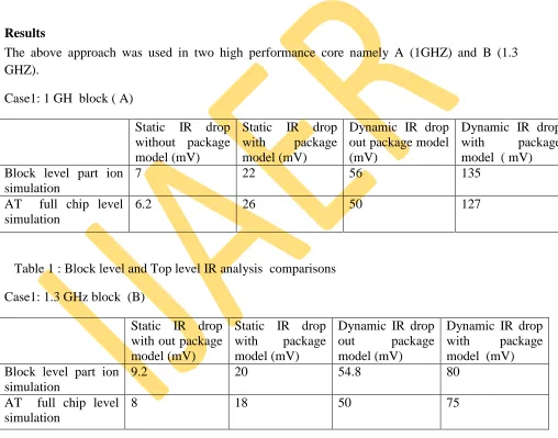
Results
The above approach was used in two high performance core namely A (1GHZ) and B (1.3 GHZ).
Case1: 1 GH block ( A)
Static IR drop without package model (mV)
Static IR drop with package model (mV)
Dynamic IR drop out package model (mV)
Dynamic IR drop with package model ( mV) Block level part ion
simulation
7 22 56 135
AT full chip level simulation
6.2 26 50 127
Table 1 : Block level and Top level IR analysis comparisons
Case1: 1.3 GHz block (B)
Static IR drop with out package model (mV)
Static IR drop with package model (mV)
Dynamic IR drop out package model (mV)
Dynamic IR drop with package model (mV) Block level part ion
simulation
9.2 20 54.8 80
AT full chip level simulation
8 18 50 75
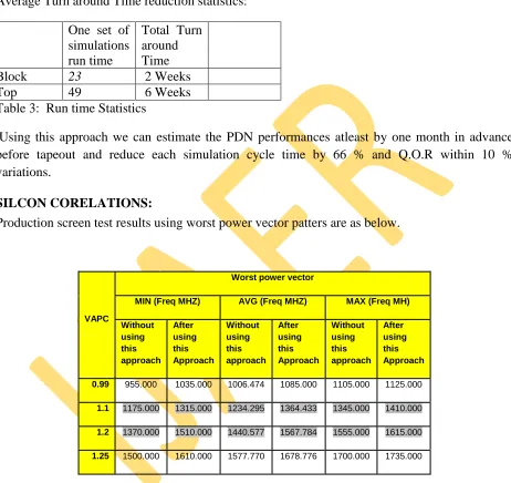
Average Turn around Time reduction statistics:
One set of simulations run time
Total Turn around Time Block 23 2 Weeks Top 49 6 Weeks Table 3: Run time Statistics
Using this approach we can estimate the PDN performances atleast by one month in advance before tapeout and reduce each simulation cycle time by 66 % and Q.O.R within 10 % variations.
SILCON CORELATIONS:
Production screen test results using worst power vector patters are as below.
Table 4: Production screen test results
The above table (Table 4) captures the min/avg/max frequency achieved at different voltage values. This is evident from above results that after using this approach we may get better silicon performances.
VAPC
Worst power vector
MIN (Freq MHZ) AVG (Freq MHZ) MAX (Freq MH)
Without using this approach
After using this Approach
Without using this approach
After using this Approach
Without using this approach
After using this Approach
0.99 955.000 1035.000 1006.474 1085.000 1105.000 1125.000
1.1 1175.000 1315.000 1234.295 1364.433 1345.000 1410.000
1.2 1370.000 1510.000 1440.577 1567.784 1555.000 1615.000
The below table capture the silicon measurements dynamic IR drop numbers measured at package pin while running worst power vectors at 998 MHz /1.2 Gh and 1.5 GHz /
VI results on high performance core (1.3 GHZ):
998 Mz 1.2Ghz 1.5 dynamic
IR drop
32 mV 35mV 40mV
Table 5: VI results.
The Table 5 indicates the package decap used in the test case for high performance block was the optimal one as no significant variations in voltage dip was seen when frequency increases from 998 Mhz to 1.5 Ghz .
CONCLUSION:
In this paper block level static and dynamic IR simulations are carried out to mimic the full chip level simulations. This approach may be used to decide the high performance block locations at full chip level , optimize the RDL route , bump pitch used , package route and package decap usages irrespective of complete full flat analysis . This helps to predict the PDN analysis much before tape out and help to optimize the PDN performances. The block level simulations are within 10 % of full chip analysis and this is really encouraging.
R
EFERENCES1. ―Block level analysis of chip and system level resonances ― – Jason Chen, Biswajit Patra, Sorin Dobre … DesignCon 2010
2. M. E. Kowalski and R. Codd, "Co-simulation of IC, Package and PCB Power Delivery Networks in Ultra-Low Voltage Power Rail Designs," 2007 Electronic Components and Technology Conference, pp. 798-803.
3. Novak, Power distribution Network Design Methodologies, IEC, 2008.