ANALYSIS OF A SELF -FORMATION PROCESS OF SEMICONDUCTOR
ELEMENTS
Donatas Saulevi
č
ius, Laimutis Telksnys
Recognition Processes Department, Institute of Mathematic and Informatics A. Goštauto 12, LT-01108 Vilnius, Lithuania
e-mail: [email protected]
Abstract. Self-formation processes of semiconductor elements are discussed. A method for recognition of self-formed semiconductor elements is described. The method based on the Region Connection Calculus theory is pro-posed. A system for recognition of semiconductor elements is developed. The experimental results of the recognition of semiconductor elements are presented.
Keywords: Pattern recognition, self-formation, semiconductor elements, qualitative spatial reasoning, Region Connection Calculus.
1. Introduction
Computer system for the self-formed artificial ob-ject classification can help accelerating selection of objects and reduce the volume of work in a decision making process. The main task for a recognizer is to analyze generated patterns – semiconductor elements – using the proposed criteria, to classify them and out-put results. The original comout-puter system for qualita-tive evaluation of semiconductor elements is based on the Region Connection Calculus (RCC) [7] theory, the particular formalism for Qualitative Spatial Reasoning [4].
The system of semiconductor elements recogni-tion, based on the C++ dot Net technology, is dis-cussed. The verification of the system was performed.
2. The Problem
Self-formation methods for creating technologies for semiconductor elements (e.g. transistors, solar cells) are based on the phenomenon of self-formation of artificial objects. Self-formation simulation results are two-dimensional geometrical figures - patterns [2, 3]. The pattern might fit for mass production, e.g., satisfy the set conditions. Consequently, the analysis of the structure of such objects is required. But recog-nition of proper self-formed artificial objects is an ex-tremely labour consuming process.
Therefore pattern recognition can help reduce the volume of work in the decision making process and in accelerating object selection – classification into two
classes, namely, class A (good semiconductor ele-ment) and class B (bad semiconductor element) [1].
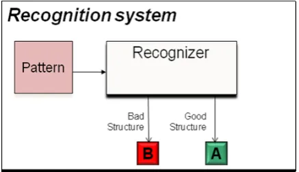
The concept of the system for recognition of semi-conductor elements is given in Figure 1.
Figure 1. Recognition system
Self-formation results – sets of semiconductor ele-ments – depend on different initial conditions, e.g., having a different geometric structure and different substances. According to these conditions, self-formed elements obtain a particular geometry, but probably don’t meet the definite electrical characteristics.
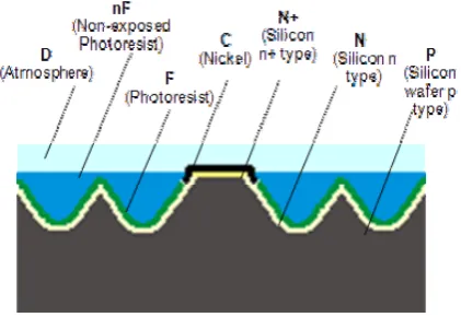
An example of artificial semiconductor element (solar cell) structure with the notation of substances is given in Figure 2.
the example patterns, but we need to approach regions of the object and relations between those regions, no matter what form of the region is.
Figure 2. Example of the structure of a semiconductor element
The system to recognize the semiconductor ele-ments, which is based on singularity of structures of the element, the rules of the relations between the regions within the structure and RCC theory [4,5,6] was developed.
3. Recognition system. Concept
The concept of recognition system is based on the RCC theory, which is used for Geographic In-formation Systems, image analysis and characterized by essential axioms.
The basis of the theory is one primitive binary relation C(x,y) read as “x connects with y” [4].
The essential axioms are as following:
1. ∀x[C(x,x)] (reflexivity); (1)
2. ∀x∀y [C(x,y) → C(y,x)] (symmetry) ; (2) 3. DC(x,y) ≡def ¬C(x,y)
(x is disconnected from y); (3)
4. EC(x,y) ≡def C(x,y) ∧¬O(x,y)
(x is externally connected to y); (4)
5. O(x,y) ≡def ∃z[P(z,x) ∧ P(z,y)]
(x overlaps y); (5)
6. P(x,y) ≡def ∀z[C(x,z) → C(z,y)]
(x is a part of y); (6)
7. EQ(x,y) ≡ def P(x,y) ∧ P(y,x)
(x is identical with y); (7)
8. CON(x) ≡def ∀yz[sum(y,z) = x → C(y,z)] (continuous), (8)
where sum(x,y) – the quasi-Boolean function sum of x and y [4].
Graphical interpretation of axioms is illustrated in Figure 3.
In conformity with RCC axioms and requirements for the structure of semiconductor elements, the rules, which show that semiconductor element belongs to class A, have been described:
CON(P) ∧ CON(C) ∧¬CON(F) ∧ EC (C,D) ∧ EC (C,N+) ∧ EC (P,N) ∧ EC (P,N+) ∧ DC(D,P) ∧ DC
(D,N+) ∧ DC (D,N) (9)
CON (P) – RegionP must be continuous.
¬CON (F)–RegionF cannot be continuous. EC (P,N) – Region P is externally connected to region N.
DC (D,P) – Region P is disconnected from region D.
Figure 3. Essential RCC axioms
An object belongs to class A if all rules (9) are met. Otherwise, the object belongs to class B. These rules are implemented within the recognizer.
The main task for a recognizer is to analyze generated patterns – semiconductor elements - by using the criteria proposed, e.g. to extract features of elements, to classify elements and to output results. The pattern is divided into chromatic regions (substances) and connections between regions are identified for feature extraction. Then, the RCC rules are checked to classify the object either into class A (when all the rules are met) or class B (otherwise).
A sequence of the actions performed by the recognizer is as follows:
• Read the object;
o System reads image pixels (RGB values) and coordinates into an array;
• Assign labels;
o System assigns a label to each pixel depending on the RGB value;
• Initialize regions;
o System initializes regions of the object while analyzing the label values of each pixel. The result is the label of the region and ID of the region;
o System identifies connections of the region with other regions;
o Conjunction of the neighbouring regions with the same label;
• Initialize rules;
• Check rules for the object; o System checks all the rules;
• Output results.
Figure 4. Processes of the recognition system
Read Image process (see Figure 4) describes image reading into an array. A specification of the process is given in Figure 5.
BMP image Read Image Normalize Object
image(x,y)
values(x,y,R,G,B,)
values(x,y,R,G,B)
values(x,y,R1,G1,B1)
Figure 5. Sequence diagram for the Read Image process In this stage the image (semiconductor element) is read into an array whose elements are RGB values of image pixels. The RGB values are generalized accor-ding to the range of colour values (Table 1). Depen-ding on the RGB range, the pixel RGB value is recalculated to the pixel label value.
Table 1. RGB values – labels
Label Substance R G B
101 P 77 73 72
103 N 255 251 156
150 C 0 0 0
105 N+ 229 222 86
0 D 210 255 255
140 F 0 210 63
141 nF 0 147 221
The Process Analyze Image (Figure 4) aggregates two particular processes – Initialize Regions and Check Rules. First of all, the system identifies image regions using the read image data (array of image pixels) (Figure 6).
The system reads regions of the image structure while analyzing the array of the image pixels. Each region is marked by the colour value – label (accor-ding to pixel value – label) and the region ID number. This number is necessary in the case where two or more not connected regions of the same colour exist within the structure. The region connection process also includes identification of connections of regions.
Figure 6. Sequence diagram for the Initialize Regions process
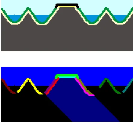
Analysis of image pixels starts from the top left pixel to the right and moves down by one pixel row in each step. Due to that, the region often might be divi-ded into more regions with the same label, but different ID. Thus, the system implements conjunction of the regions. The original view of a semiconductor element and the same element with a few regions coloured after the region initialization step is presen-ted in Figure 7. In this example, 12 different regions are coloured (other regions are in black), but lots of them will be conjugated later (see Figure 7).
Figure 7. Initial result of regions initialization Connected regions with the same label but different ID values will be conjugated.
diagram of the process Check Rules is presented in Figure 8.
Object RCC Rules
CheckRules()
InterpretRule(RULE) ReadRule()
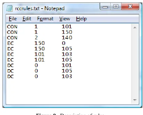
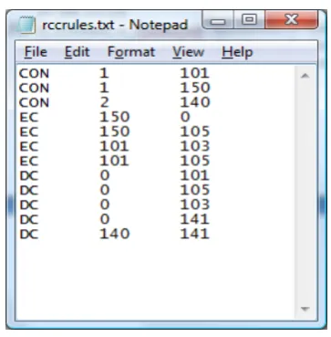
Figure 8. Sequence diagram of the process Check Rules In this stage, application reads the RCC. Rules are specially described in an external text file. The rules may vary according to the type of semiconductor ele-ment, the structure of composing substances (regions) and connections between them. Thus, the recognition system might be used in various occurrences of self-formation (Figure 9).
Figure 9. Description of rules
All the rules, which were read, are applied to the analysis of region.
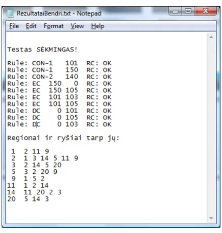
After the check of the rules, system outputs a mes-sage to the user if a semiconductor element meets the rules described (see Figure 11). The results are printed into a text file, as well.
4. Software and Experiments
Based on the concept of the system given above, the software application „BMPRCC1“for the recogni-zing semiconductor elements was realized. The soft-ware for recognizing semiconductor elements is based on C++ dot Net technology. This software is designed for analysing bmp files.
The test results show that recognition of one element takes about 100 milliseconds. The computer parameters for testing software were as follows:
• Processor: Intel(R) CoreTM 2 CPU, 6600 @ 2,4 GHz, 2 Cores, 2 Logical Processors; 8192 Kb cache memory
• Physical Memory (RAM): 2,00 GB
• OS Name: Microsoft(R) Windows WistaTM Ultimate
In the first step, the system reads a semiconductor element into the array of RGB values of the pixels. Subsequently RGB values of the pixels are generali-zed and the system outputs a re-coloured image to the user (this is necessary when the quality of images is different or rough) (Figure 10).
Figure 10. “BMPRCC1“application window: re-coloured image
In the next step, all the image analysis processes are implemented: regions extraction, rules interpreta-tion, and results output (Figure 11).
Figure 11. Recognition result
As we see in an example, which is given in Figure 11, the software outputs a message about a failed test. The regions of semiconductor element don’t meet the described connection rules – the structure of the semi-conductor element is not suitable.
The system forms the file of test results with the comprehensives results for each test (see Figure 12):
are not connected and substances C and N+ (silicon n+ type) are not connected.
Figure 12. File of the recognition results (1) The result of a successful test is given in Figure 13.
Figure 13. File of the recognition results (2) As we see in Figure 13, all the required rules are met. The test has passed with the verdict true.
The digits in the results file below the rules (Figure 13) mean (from the left): the region number (not the substance notation) and identifiers of regions connected with that region.
This system is flexible for recognizing of any self-formed (and not only) two-dimensional structures if the suitability of the elements can be described by substances which participate within the structure and by connections between the substances. Thus, this system might be adapted to a particular case with no changes of the algorithm.
The main steps of adapting the system for recogni-zing of particular set of semiconductor elements are: 1. Substance identification:
a. Identification of colour for each substance; b. Determination of the colour values range (if
necessary);
c. Identification of substances (notation assig-ning);
2. Description of the connections between the regions (rules are defined to describe the regions connections).
It is necessary to describe a few initial variables to identify substances:
1. value[x] – array of substances colour 2. label[x] – array of substances colour notation 3. RULE_NAME[ ] – array of rules
The common algorithm to identify regions and to check the rules is as follows:
k=0; RN=1;
BEGIN (k, label) {
region[k][value]=value[x]
region[k][value][label]= label[x]
CHECK COLOR (k) {
FOR (i=0; i<8; i++) {
IF (Neighbour[i][value] != region[k][value])
{
region[k][value][neighbour][i][value] = Neighbour[i][value]
j=j+1 } }
IF (j==8) GO TO BEGIN(k+1, label[x+1]) ELSE GO TO SET LABEL (k)
}
SET LABEL(m) {
FOR (i=0; i<8; i++) {
IF ( Neighbour[i][value] == region[k][value] )
{ m=m+1;
region[m][value] = region[k][value] region[m][value][label] =
region[k][value][label] }
}
CHECK COLOR(m+1) }
}
RULE_NAME[ ] = { CON(1,P); CON(1,C); EC(C,D); EC(C,N+); ... }
FOREACH (m) {
IF (RULE_NAME[m] == TRUE) {
RN=RN+1
Print (RESULT: RULE_NAME = true) }
ELSE {
Print (RESULT: RULE_NAME = false) }
}
IF (RN < RuleNumber) Print (IMAGE BELONGS TO CLASS B)
ELSE Print (IMAGE BELONGS TO CLASS A)
//////////////RULE FUNCTIONS
CON(number,y) {
IF (number==0) {
IF(count(region[y][]) > 1 ) RETURN TRUE
} ELSE {
IF(count(region[y][]) == number ) RETURN TRUE
} }
EC(x,y) {
FOREACH(i,j, k) {
IF(region[i][y][neighbour][k][value] == region[j][x]) RETURN TRUE
} }
DC(x,y) {
FOREACH(i,j, k) {
IF(region[i][y][neighbour][k][value] == region[j][x]) RETURN FALSE
} }
In our case the primal variables are: value[1] = 77,73,72;
value[2] = 255,251,156; value[3] = 0,0,0; value[4] = 229,222,86; value[5] = 210,255,255; value[6] = 0,210,63; label[1] = 101; label[2] = 103; label[3] = 150;
label[4] = 105; label[5] = 0; label[6] = 140;
The connection rules for the semiconductor ele-ment are (from Figure 9):
RULE_NAME[1] = CON(1,105); RULE_NAME[2] = CON(1,104); RULE_NAME[3] = CON(2,106); RULE_NAME[4] = EC(105,106); RULE_NAME[5] = EC(104,106); RULE_NAME[6] = DC(104,105); RULE_NAME[7] = DC(104,0); RULE_NAME[8] = DC(105,0);
5. Recognition results
A total of 851 self-formed semiconductor elements have been analyzed while the experimental test was accomplished. In this experiment solar cells have been evaluated.
The test assigned 23 solar cells to class A. Results of the experiment are given in Table 2.
Table 2. Recognition results of solar cells (1) Total Class “A” Class “B”
851 23 828
100% 2,7% 97.3%
Initial conditions were supplemented with a few new rules for testing the system flexibility. Let us suppose that the structure of semiconductor element is suitable if all the rules (given in Figure 9) are met. The additional conditions - regions D and F cannot be connected with region nF (see Figure 2) – should be satisfied. Then the connection rules are as follows:
CON(P) ∧ CON(C) ∧¬CON(F) ∧ EC (C,D) ∧ EC (C,N+) ∧ EC (P,N) ∧ EC (P,N+) ∧ DC(D,P) ∧ DC (D,N+) ∧ DC (D,N) ∧ DC (D,nF) ∧ DC (F,nF) (10)
The file of rules is supplemented with two new rules (Figure 14).
The recognition test has assigned 6 solar cells to class A. The results of the experiment are summarized in Table 3.
6. Conclusions
Figure 14. File of the extended set of rules
Table 3. Results of solar cells recognition (2)
Total Class “A” Class “B”
851 6 845
100% 0,71% 99.29%
To conclude, we state:
• The processes of self-formation of the artificial semiconductor elements are discussed.
• The method, algorithm and software for recogni-tion of the self-formed semiconductor elements have been developed.
• Experimental tests of recognition of semiconduc-tor elements with two sets of connection rules have been performed.
• The experimental results prove that the developed recognition system is suitable for recognition of the self-formed semiconductor elements.
References
[1] L. Telksnys. Self-Formation Supported by Pattern Recognition. Proceedings of the 6th International Con-ference on Self-Formation Theory and Applications, ISSN 1012-0394. Solide State Phenomena, 2004, Vols. 97-98, 51-58.
[2] S. Janusonis Self-formation of the Artificial Planar Systems. What is it? In: Self-formation Theory and Applications. Proceedings of the 6th International Conference Self-formation Theory and Applications, Vilnius, Lithuania, November 26-28, 2003, Solid State Phenomena, 2004, Vols. 97-98, 11-20.
[3] L. Leonas, S.Janusonis Simulation of Self-formation in Solar cell Technology. Self-formation Theory and Applications. Proceedings of the 6th International Conference Self-formation Theory and Applications, Vilnius, Lithuania, November 26-28, 2003, Solid State Phenomena, 2004, Vols. 97-98, 103-108.
[4] A.G. Cohn, B. Bennett, J.M. Gooday, N.M. Gotts.
Representing And Reasoning With Qualitative Spatial Relations About Regions. Spatial and Temporal Reasoning, 1997, 97-134.
[5] D.A. Randell, A.G. Cohn. Modelling Topological and Metrical Properties in Physical Processes. Procee-dings 1st International Conference on the Principles of Knowledge Representation and Reasoning, edited by Brachman, R and Levesque, H and Reiter, R, Mor-gan Kaufmann, Los Altos, 1989, 357-368.
6] D.A. Randell, Z. Cui, A.G. Cohn. A Spatial Logic Based on Regions and Connection. Proc. 3rd Int. Con-ference on Knowledge Representation and Reasoning, edited by Nebel B and Rich C and Swartout W, Mor-gan Kaufmann, San Mateo, 1992, 165-176.
[7] B.L. Clarke. A calculus of individuals based on ‘con-nection’. Notre Dame Journal of Formal Logic. 1981, Vol. 22, No.3, 204-218.