A New Implementation of CMOS Full-Adders for
Energy-Efficient Arithmetic Applications
S. Madhava Rao
VRS & YRN College of Eng& Tech Chirala, Prakasam (DT), A.P.
Prof. K. Amarnath
VRS & YRN College of Eng& TechChirala, Prakasam (DT), A.P. [email protected]
V. Santhisri
VRS & YRN College of Eng& Tech Chirala, Prakasam (DT), A.P.
Abstract - We present two high-speed and low-power full-adder cells designed with an alternative internal logic structure and pass-transistor logic styles that lead to have a reduced power-delay product (PDP). We carried out a comparison against other full-adders reported as having a low PDP, in terms of speed, power consumption and area. All the full-adders were designed with a 0.18- m CMOS technology, and were tested using a comprehensive test bench that allowed to measure the current taken from the full-adder inputs, besides the current provided from the power-supply. Post-layout simulations show that the proposed full-adders outperform its counterparts exhibiting an average PDP advantage of 80%, with only 40% of relative area.
Keywords — Arithmetic, full-adder, high-speed, low-power.
I. I
NTRODUCTIONEnergy efficiency is one of the most required features for modern electronic systems designed for high-performance and/or portable applications. In one hand, the ever increasing market segment of portable electronic devices demands the availability of low-power building blocks that enable the implementation of long-lasting battery-operated systems. On the other hand, the general trend of increasing operating frequencies and circuit complexity, in order to cope with the throughput needed in modern high-performance processing applications, requires the design of very high-speed circuits. The power-delay product (PDP) metric relates the amount of energy spent during the realization of a determined task, and stands as the more fair performance metric when comparing optimizations of a module designed and tested using different technologies, operating frequencies, and scenarios.
Addition is a fundamental arithmetic operation that is broadly used in many VLSI systems, such as application-specific digital signal processing (DSP) architectures and microprocessors. This module is the core of many arithmetic operations such as addition/subtraction, multiplication, division and address generation. As stated above, the PDP exhibited by the full-adder would affect the system’s overall performance [1]. Thus, taking this fact into consideration, the design of a full-adder having low-power consumption and low propagation delay results of great interest for the implementation of modern digital systems. In this paper, we report the design and performance comparison of two full-adder cells implemented with an alternative internal logic structure, based on the multiplexing of the Boolean functions XOR/ XNOR and AND/OR, to obtain balanced delays in SUM and CARRY outputs, respectively, and pass-transistor
powerless/groundless logic styles, in order to reduce power consumption. The resultant full-adders show to be more efficient on regards of power consumption and delay
Fig.1. Full-adder cell formed by three main logical blocks. When compared with other ones reported previously as good candidates to build low-power arithmetic modules. This paper is organized as follows. Section II presents the internal logic structure adopted as standard in previous papers for designing a full-adder cell. Section III introduces the alternative internal logic structure and the pass-transistor powerless/groundless logic styles used to build the two proposed full-adders. Section IV explains the features of the simulation environment used for the comparison carried out to obtain the power and speed performance of the full-adders. Section V reviews the results obtained from the simulations, and Section VI concludes this work.
II. P
REVIOUSFULL-A
DDERO
PTIMIZATIONSMany papers have been published regarding the optimization of low-power full-adders, trying different options for the logic style (standard CMOS [2], differential cascade voltage switch (DCVS) [3], complementary pass-transistor logic (CPL) [4], double pass-pass-transistor logic (DPL) [5], swing restored CPL (SR-CPL) [6], and hybrid styles [and the logic structure used to build the adder module. The internal logic structure shown in Fig. 1 has been adopted as the standard configuration in most of the enhancements developed for the 1-bit full-adder module. In this configuration, the adder module is formed by three main logical blocks: a XOR-XNOR gate to obtain AB
Copyright © 2012 IJECCE, All right reserved delay and, in most of the cases, the power consumption of
the full-adder depend on the delay and voltage swing of theABsignal and its complement generated within the cell. So, to increase the operational speed of the full-adder, it is necessary to develop a new logic structure that does not require the generation of intermediate signals to control the selection or transmission of other signals located on the critical path.
III. A
LTERNATIVEL
OGICS
TRUCTURE FORA
F
ULL-A
DDERExamining the full-adder’s true-table in Table I, it can be seen that the So output is equal to the ABvalue when C=0, and it is equal to AB when C=1. Thus, a multiplexer can be used to obtain the respective value taking the C input as the selection signal. Following the same criteria, the Co output is equal to the A•B value when C=0 , and it is equal to A+B value when C=1. Again, C can be used to select the respective value for the required condition, driving a
Fig.2. Alternative logic scheme for designing full-adder cells.
TABLE I
TRUE-TABLE FOR A 1-BIT FULL-ADDER: A, B, AND C ARE INPUTS; SO AND CO ARE OUTPUTS
multiplexer. Hence, an alternative logic scheme to design a full-adder cell can be formed by a logic block to obtain the ABand AB signals, another block to obtain the A•B and A+ B signals, and two multiplexers beingdriven by the C input to generate the So and Co outputs, as shown in Fig. 2 [13]. The features and advantages of this logic structure are as follows.
• There are not signals generated internally that control the selection of the output multiplexers. Instead, the C input signal, exhibiting a full voltage swing and no extra delay, is used to drive the multiplexers, reducing so the overall propagation delays.
• The capacitive load for the C input has been reduced, as it is connected only to some transistor gates and no longer to some drain or source terminals, where the diffusion capacitance is becoming very large for sub-micrometer technologies. Thus, the overall delay for larger modules where the C signal falls on the critical path can be reduced.
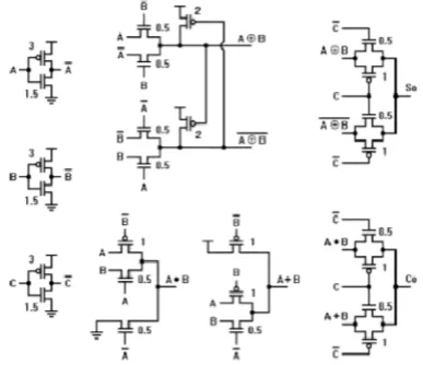
• The propagation delay for the So and Co outputs can be tuned up individually by adjusting the XOR/XNOR and the AND/OR gates; this feature is advantageous for applications where the skew between arriving signals is critical for a proper operation (e.g., wave pipe lining), and for having well balanced propagation delays at the outputs to reduce the chance of glitches in cascaded applications. Based on the results obtained in [13], two new full-adders have been designed using the logic styles DPL and SR-CPL, and the new logic structure presented in Fig. 2. Fig. 3 presents a full-adder designed using a DPL logic style to build the XOR/XNOR gates, and a pass-transistor based multiplexer to obtain the So output. In Fig. 4, the SR-CPL logic style was used to build these XOR/XNOR gates. In both cases, the AND/OR gates have been built using a powerless and groundless pass-transistor configuration, respectively, and a pass-transistor based multiplexer to get the Co output.
Fig.3. Full-adder designed with the proposed logic structure and a DPL logic style (Ours1).
IV. I
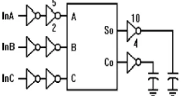
MPLEMENTATIONFig. 5 shows the test bed used for the performance analysis of the full-adders. This implementation has been used for comparing the full-adders analyzed in [9], [14], with the addition of the inverters at the outputs. The size of the input buffers lets to experience some degradation in the input signals, and the size of the output buffers equals the load of four small inverters for this technology. This test bed is presented as a generalization of static CMOS gates driving and been driven for the full-adder cell under test. The main advantage of using this simulation environment is that the following power components are taken into account, in addition to the dynamic one.
• The short-circuit consumption of the inverters connected to the device under test (DUT) inputs. This power consumption varies according to the capacitive load that the DUT offers at the inputs. Furthermore, the energy required to charge and discharge the DUT
Fig.5. Test bed used for simulating the full-adders under comparison.
Internal nodes when the module has no direct power supply connections (as for the case of pass-transistor logic styles), comes through these inverters connected at the DUT inputs.
• The short-circuit consumption of the DUT by itself, as it is receiving signals with finite slopes coming from the buffers connected at the inputs, instead of ideal ones coming from voltage sources.
• The short-circuit and static consumption of the inverters connected to the outputs of the DUT, which are due to the finite slopes and degraded voltage swing of the full-adder output signals. The importance of including the effects and power consumption of the buffers connected at the inputs and outputs of the DUT, comes from the fact that the DUT is always going to be used in combination with other devices to build a larger system, and these static inverters are a good generalization for any operating scenario to be considered. For the stimulus vectors, we used the test inputs patterns recommended in [1], as they exercise all the input combinations necessary to determine the worst case propagation delay and power consumption values.
V. S
IMULATIONR
ESULTSWe compared the performance of 7 full-adders, named: new14T [15], hpsc [7], hybrid [8], hybrid cmos [9], cpl [10], Ours1 and Ours2. The schematics and layouts were
simulated using the BSIM3v3 model (level 49)and the post-layout.
Simulations were carried out using Nanosim [16] to determine the power consumption features of the designed full-adders, and Hspice [17] to measure the propagation delay for the output signals. In order to have a fair comparison, we took the transistors sizes for each full-adder that were reported in the correspondent paper, and made all the layouts with a homogeneous arrangement.
Fig. 6. Layout of the proposed full-adder Ours1
All the full-adders were supplied with 1.8 V and the maximum frequency for the inputs was 200 MHz. This table reports the results for the whole test bed (top) and for the full-adder alone (add). It is worth to observe that in some cases, the power consumed from the power-supply (pwr supply) for the full-adder is smaller than the total average power (avg power). This is because of, for some logic styles (e.g., pass-transistor style), some current is taken from the inputs of the full-adder and is used to charge the internal nodes. As mentioned above, it is the importance of considering the power consumption of the input buffers in the top test-bed. we can state the following.
• Only two full-adders exhibit static-dissipation. These are the new14T and cpl adders, which are implemented with logic styles that have an incomplete voltage swing in some internal nodes, causing this consumption component. • The power consumption improvements of the full-adders taken in descending order correlate with the optimizations reported.
Copyright © 2012 IJECCE, All right reserved 60%, and considering the consumption of the standalone
full-adder the savings are up to 80%. These savings can be justified by the joint reduction of dynamic and short-circuit power components.
• The short-circuit consumption optimization is related to the powerless/ groundless configuration of the constituent AND/OR gates, and the dynamic consumption optimization comes from the fact of reduced capacitances in the internal nodes for pass-transistor logic styles, and for the well balanced propagation delays inside the full-adder, which results in less glitches at the outputs.
• With regardsof the speed, it can be seen the advantage of the logic structure introduced here, since both realizations designed using this scheme (Ours1 and Ours2) exhibit the smallest propagation delay, only matched by the cpl full-adder. It shows a propagation delay improvement around 25% compared with the new14T and hpsc full-adders. • The power-delay product (PDP) column confirms the energy-efficiency for the full-adders built using the new internal logic structure. They present the lowest PDP metric, up to 85% of saving, due to the combined reduction of power consumption and propagation delay. • In addition, we carried out separated simulations to determine the lowest power supply voltage that each full-adder can tolerate, while keeping its correct functionality. As shown in column “Vdd min”, the proposed full-adders can operate properly with voltage supplies as low as 0.6 V. Since these realizations have neither static consumption, nor internal direct paths from Vdd to Gnd (except for the inverters at the inputs, which could be avoided if the inputs come from FF’s with complementary outputs), they are good candidates for battery-operated applications where low consumption modules with standby modes are required.
• The importance of the simulation setup and the inclusion of the power consumption components for the surrounding circuitry are evident, as some realizations reported previously as low-power cells have been shown to perform worse than other ones when considering the power consumption of the whole test-bed.
• On regards of the implementation area obtained from the layouts, it can be seen that the proposed full-adders require the smallest area (up to 40% of relative area), which can also be considered as one of the factors for presenting lower delay and power consumption, as it implies smaller parasitic capacitances being driven inside the full-adder. The reason for the smaller area, compared to other full-adders that have less transistors, is that the size of the transistors in the proposed full-adders is minimal and not larger than 2 m (except for the symmetrical response inverters at the inputs), while for other full-adders the transistor sizes are in the range of 4 to 6 m. Figs. 6 and 7 show the layouts of the proposed full-adders, with the correspondent side by side dimensions.
• Finally, we determined the maximum frequency that each full adder can operate, while being supplied with 1.8 V. The proposed full-adders reach up to 1.25 GHz, only surpassed by cpl cell, at the expense of major power consumption and area. The reason for running the
power-delay performance simulations at 200 MHz was due to the full adders that work only up to 250 MHz.
V.I. O
UTPUTE
AVEFORMSIn fig. 7.1 the simulation results for this full adder Hybrid CMOS has shown in this waveform as all inputs are applying with same rise time, fall time, pulse value and frequency. Hence the three inputs are merged into single waveform. It can be observed in the first waveform. The simulation is carried out at 200 MHZ frequency. Post layout simulation for this full adder shows the overall power dissipation is 102.5 nano watts. The delay is 182.7 pico seconds for sum output and 149 pico seconds for carry output. The average delay for this full adder is 145.3 pico seconds.
Fig.7.1 Output waveforms of the HYBRID CMOS full adder
VI. C
ONCLUSIONAn alternative internal logic structure for designing full-adder cells was introduced. In order to demonstrate its advantages, two full-adders were built in combination with pass-transistor powerless/groundless logic styles. They were designed with a TSMC 0.18- m CMOS technology, and were simulated and compared against other energy-efficient full-adders reported recently. H spice and Nano sim simulations showed power savings up to 80%, and speed improvements up to 25%, for a joint optimization of 85% for the PDP. The area utilization for the proposed full-adders is only 40% of the largest full-adder compared, and the power-supply voltage for the proposed full-adders can be lowered down to 0.6 V, maintaining proper functionality.
R
EFERENCES[1] A. M. Shams and M. Bayoumi, “Performance evaluation of 1-bit
CMOS adder cells,” in Proc. IEEE ISCAS, Orlando, FL, May
1999, vol. 1, pp. 27–30.
[2] N. Weste and K. Eshraghian, Principles of CMOS VLSI Design, A System Perspective. Reading, MA: Addison-Wesley, 1988, ch.
[3] K. M. Chu and D. Pulfrey, “A comparison of CMOS circuit
techniques: Differential cascode voltage switch logic versus
conventional logic,”IEEE J. Solid-State Circuits, vol. SC-22, no.
[4] K. Yano, K. Yano, T. Yamanaka, T. Nishida, M. Saito, K.
Shimohigashi, and A. Shimizu, “A 3.8 ns CMOS 16 16-b
multiplier using complementary pass-transistor logic,” IEEE J. Solid-State Circuits, vol. 25, no. 2, pp. 388–395, Apr. 1990. [5] M. Suzuki, M. Suzuki, N. Ohkubo, T. Shinbo, T. Yamanaka, A.
Shimizu, K. Sasaki, and Y. Nakagome, “A 1.5 ns 32-b CMOS
ALU in double pass-transistor logic,” IEEE J. Solid-State Circuits, vol. 28, no. 11, pp. 1145–1150, Nov. 1993.
[6] R. Zimmerman and W. Fichtner, “Low-power logic styles:
CMOS versus pass-transistor logic,” IEEE J. Solid-State Circuits, vol. 32, no. 7, pp. 1079–1090, Jul. 1997.
[7] M. Zhang, J. Gu, and C. H. Chang, “A novel hybrid pass logic
with static CMOS output drive full-adder cell,” in Proc. IEEE Int. Symp. Circuits Syst., May 2003, pp. 317–320.
[8] C. Chang, J. Gu, and M. Zhang, “A reviewof 0.18- mfull adder
performances for tree structured arithmetic circuits,” IEEE
Trans. Very Large Scale Integr. (VLSI) Syst., vol. 13, no. 6, pp. 686–695, Jun. 2005.
[9] S. Goel, A. Kumar, and M. Bayoumi, “Design of robust, energy
-efficient full adders for deep-submicrometer design using
hybrid-CMOS logic style,” IEEE Trans. Very Large Scale Integr.
(VLSI) Syst., vol. 14, no. 12, pp. 1309–1320, Dec. 2006.
[10] S. Agarwal, V. K. Pavankumar, and R. Yokesh, “Energy
-efficient high performance circuits for arithmetic units,” inProc.
2nd Int. Conf. VLSI Des., Jan. 2008, pp. 371–376.
A
UTHOR’SP
ROFILES. Madhava Rao
received B.Tech. degree in Electronics and Communications Engineering from JNTU University, Kakinada, in 2002, Currently doing M. Tech. in VRS&YRN Engineering college,
from JNTUK University, Kakinada. His research interests include wireless, VLSI and Embedded systems. He is the author of more than 5 papers
K. Amarnath
received B.E. degree in Electronics and Communications Engineering from Channai University, received M.E. from Sathyabhama University and currently he working as an Professor& HOD, Dept of ECE in V.R.S. & Y.R.N. Engg. College, Chirala.