Design and Implementation of Standby Leakage Power
Reduction Technique for Nano scale CMOS VLSI
Systems
P.Srinivasulu.Asst.Prof. ECE Dept. DR.SGIET, Markapur [email protected]
R.V.Kiran kumar M.Tech student t[DECS]
DR.SGIET Markapur [email protected]
Dr. K.Srinivasarao Principal
TRR College of Engineering &Tech, Hyderabad
Dr. A.Vinaya Babu Principal
JNTUH college of engineering, Hyderabad
Abstract – In this paper, a novel low-power design technique is proposed to minimize the standby leakage power in nanoscale CMOS very large scale integration (VLSI) systems by generating the adaptive optimal reverse body-bias voltage. The adaptive optimal body-bias voltage is generated from the proposed leakage monitoring circuit, which compares the subthreshold current (ISUB) and the
band-to-band tunneling (BTBT) current (IBTBT). The proposed circuit
was simulated in HSPICE using 32-nm bulk CMOS technology and evaluated using ISCAS85 benchmark circuits at different operating temperatures (ranging from 25 ◦C to 100 ◦C). Analysis of the results shows a maximum of 551 and 1491 times leakage power reduction at 25 ◦C and 100 ◦C, respectively, on a circuit with 546 gates. The proposed approach demonstrates that the optimal body bias reduces a considerable amount of standby leakage power dissipation in nanoscale CMOS integrated circuits. In this approach, the temperature and supply voltage variations are compensated by the proposed feedback loop.
Keywords – Band-to-band tunneling (BTBT) leakage, gate leakage, leakage current, leakage power, optimal body bias voltage, subthreshold leakage.
I. I
NTRODUCTIONOver the past four decades, the size of transistors has continuously been reduced to increase the device speed and density on a given chip and the die yield during manufacturing For device reliability and constant power dissipation per unit area, the supply voltage has been reduced as well. Therefore, continuous reduction in the threshold voltage of the transistor, which ensures high drive current and hence performance improvements, is inevitable [1].Recently, however, as the supply voltage approaches 1 V, conventional scaling has deviated from ideal constant-field scaling due to the difficulty of further lowering the threshold voltage (Vth). This fundamental problem stems from the nonscalable characteristic of the thermal voltage (VT = kT/q), which causes relatively fixed subthreshold swing (S) at the constant temperature. This, in turn, makes the subthreshold leakage current exponentially increase as the Vth reduces. Therefore, there exists a lowest possible value of Vth, which is determined by the application constraints related to power consumption and circuit functionality. In addition, with the knowledge of increased Vth variation in nanoscale MOSFETs, it is necessary to keep enough margins for Vth variation to ensure that Vth stays well away from the lowest possible value of Vth [3]. In particular, for high-performance (HP) logic technology, it is required to keep a
certain level of the overdrive voltage (VDD − Vth), which determines the drive current and hence the performance in a chip. This makes it difficult to accomplish the further scaling down of the supply voltage. Fig. 1 shows the difficulty of further supply voltage scaling [3]. Under fixed Vth, the reduction of VDD trades off performance (speed) and leakage power. This trend in technology scaling has made us enter a new era in achieving HP under constrained power. Fig. 2 shows the power density trends for active and standby leakage power for different channel lengths [5].Among the leakage power reduction techniques, the reverse body biasing (RBB) technique, which increases the threshold voltage (Vth) of transistors during standby mode, has widely been employed to suppress the subthreshold leakage
Fig.1. Trend of supply voltage and threshold voltage scaling
Fig.2. Power density trends for the active power and the standby leakage power with CMOS (channel length) scaling
current (ISUB). However, this technique also aggravates short channel effects (SCEs), such as drain-induced barrier lowering (DIBL), gate-induced drain leakage (GIDL), and band to- band tunneling (BTBT) current. In particular, GIDL and BTBT current significantly increase under the reverse body bias condition since the state-of-the-art MOSFETs are fabricated with high overall doping concentration, lowered source/drain junction depths, halo doping, high-mobility channel materials, etc. Furthermore, the reduction of the gate oxide thickness (tox) causes a drastic increase in the gate tunneling leakage current due to carriers tunneling through the gate oxide, which is a strong exponential function of the voltage magnitude across the gate oxide [2], [9]. Consequently, to minimize the leakage power in standby mode, those leakage components have to be taken into account when the RBB technique is used. The adaptive RBB technique has been proposed [6]–[9]. However, the previous techniques require significant circuit modification and performance overhead for leakage reduction, and they have not been complete or robust enough to apply to very large scale integration (VLSI) systems since all the leakage-current components and minimum supply voltage are not considered for leakage power reduction. While [16] shows that the leakage power can significantly be decreased using both optimum power supply voltage and optimal body bias voltage, it requires a lot of circuit overhead. Therefore, this paper proposes a new standby leakage power reduction technique applicable to VLSI systems by exploiting the body bias voltage scaling only while all the other leakage currents are taken into account. The proposed approach significantly reduces the required hardware compared with [16] by optimizing the body bias voltage only at the cost of efficiency of the standby current minimization.
II. S
TANDBYL
EAKAGEC
URRENTC
OMPONENTSINMOSFET
U
NDERRBB
(R
EVERSEB
ODYB
IAS)
Fig.3 shows the leakage current (Ileakage) components under the reverse body-bias condition. The total leakage current in the OFF-state n-MOSFET is given by
where ISUB is the subthreshold leakage current,
IBTBT(DB) and IBTBT(SB) are the BTBT leakage currents (drain-to-bulk and source-to-bulk reverse-bias p-n junction leakage currents),IGIDL(DB) and IGIDL(SB) are the GIDL currents, IGB is gateto- bulk oxide tunneling leakage current, and IDG is drain-togate oxide tunneling leakage current. The subthreshold leakage current is the weak inversion conduction current dominated by the diffusion current flowing between the drain and the source when |VGS| < |Vth|. This weak inversion conduction current can be expressed based on [11]
the depletion region under the gate area, εsi is the permittivity of Si, q is the electron charge, Nsub is the doping concentration of the p-substrate, φB is the built-in potential, VT is the thermal voltage that is equal to kT/q,
Cox is the oxide capacitance per unit area between the gate metal and the bulk surface, and n is the subthreshold parameter and is expressed as 1 + Cdep/Cox.As shown in (2), when the MOSFET is off (VGS = 0 V),the subthreshold current exponentially increases with the decrease of the threshold voltage. On the other hand, the transistor threshold voltage equation considering the body effect is given by
is the Fermi potential and is equal to (kT/q) ln(Nsub/ni), where ni is the intrinsic electron concentration, and VSB is the source-to-bulk potential difference. Since the subthreshold leakage current (ISUB) is the major leakage component, the RBB technique is used in this paper to reduce the total leakage current in standby-mode CMOS circuits by increasing the transistor threshold voltage. However, it is important to watchow other leakage current components change when the RBB is used to estimate the total leakage.
The BTBT leakage current, which is also called reverse bias p-n junction leakage currents, is the current flow between the source/drain (S/D) and the substrate through the parasitic reverse-biased p-n junction diode during the OFF-state MOSFET. If both S/D and substrate regions are heavily doped, then BTBT significantly increases since the electric field across the junction depletion region increases. If the high electric field(> 106 V/cm) is formed across the reverse-biased junctions of the source/drain (S/D) regions so that the voltage drop across the junction is bigger than the band gap of silicon, particularly with increasing S/D voltage or reverse body bias, then a significant amount of BTBT current flows through the S/D to the substrate junctions. In nanometer devices, higher channel and S/D doping with shallow junction depths are required to minimize SCEs, which cause a significant increase in BTBT current [10].
twisting of band gaps. With higher supply voltage, thinner oxide thickness, lightly doped drain, reverse body bias (RBB) technique, and high mobility channel materials having smaller band gaps, the GIDL current is enhanced [12], [13].IGB is the gate-to-bulk oxide tunneling leakage current, andIDG is the drain-to-gate oxide tunneling leakage current. As the gate oxide thickness scales below 2 nm, the direct tunneling(DT) gate leakage exponentially increases due to quantum mechanical tunneling. The DT gate leakage current can not only increase the standby power dissipation but also limit the proper logic gate operation. Recently, a high-k dielectric base on Hafnium and dual metal gate has been introduced to increase the transistor performance. The high-k dielectric material reduces the gate leakage as the gate dielectric thickness can actually be increased while the gate capacitance is increased [14].
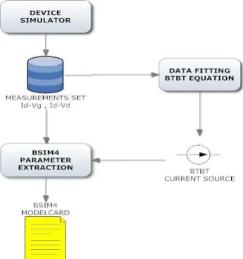
Fig. 4: BTBT source added to BSIM4 DC equivalent circuit
BTBT device
BTBT compact model was developed according to the workflow illustrated in fig. 4:
The objective of this work has been to implement a compact BTBT model readily integrable into BSIM4 to improve the accuracy of SPICE simulations. The final model is a voltage controlled current source whose analytical expression describes the BTBT phenomenon and its dependence from bias conditions. The new current source can be placed in a SPICE net list between drain and bulk terminals . m1 drain gate source bulk nmos W=1u L=65n b1 drain bulk I = Ibtbt(v(drain, bulk))
1. BTBT effects analysis with TCAD simulations of a nanometric MOSFET;
2. Development of an analytical expression for BTBT and fitting of the expression on TCAD simulations using a mathematical optimization software;
3. BSIM4 parameter extraction based on I-V curves from TCAD simulations.
-level
III. O
PTIMALB
ODY-B
IASV
OLTAGEA
NDS
UPPLYV
OLTAGEAs explained in the previous section, the main components of standby leakage power are the gate tunneling leakage power, the subthreshold leakage power, and the reverse biased junction BTBT leakage power. For convenience, let us denote that IBTBT1 = IGIDL(DB) +
IBTBT(DB), IBTBT2 =IGIDL(SB) + IBTBT(SB), Igate =
IGB + IDG, and IBTBT =IBTBT1 + IBTBT2. Therefore, the total standby leakage poweris given by
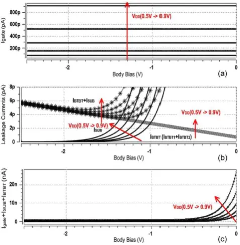
where V gate, VSUB, and VBTBT are the voltage sources of each leakage component. Fig. 4 shows the effect of body bias voltage and supply voltage on the standby leakage current for a 32 nm n-MOSFET Berkeley Predictive Technology Model. The gate leakage current is not significantly affected by VBody since IDG is not function of VBody, as shown in Fig. 4(a) [9]. However, it exponentially increases with the increase of the supply voltage. In Fig. 4(b), as the supply voltage decreases from 0.9 to 0.5 Vand the body bias voltage (VBody) decreases from 0 to −2.5 V, the subthreshold leakage current decreases while the BTBT leakage current increases. As shown in (2), the subthreshold leakage current is an exponential function of the threshold voltage (Vth). Therefore, the RBB technique is an effective way to increase the threshold voltage (Vth) to suppress the subthreshold leakage current (ISUB) in standby-mode CMOS circuits. With the increase of reverse body bias,
VSB becomes more positive, which results in higher threshold voltage and hence exponential decrease of the subthreshold current, as explained in (2) and (3). The plot of IBTBT + ISUB in Fig. 4(b) explains why the leakage power consumption of a chip does not continue to monotonically decrease with increasing reverse body bias.
Fig. 5 shows the effect of body bias voltage and supply voltage on the leakage power for an NMOS transistor of 32-nm CMOS technology. At around −0.8 to −2.2 body bias voltage, the leakage power increases due to the highly increased IBTBT. Igate has less effect on the power variation. As a result, there is an optimal reverse body bias point that makes the minimal total standby leakage power of a device for each different supply voltage.
Therefore, the optimal body bias voltage that reduces the total leakage current is determined by the relationship between
ISUB and IBTBT. In [6], ISUB and IBTBT are given in simplified form as follows:
Note that Igate is ignored because the gate tunneling leakage changes little as VBody changes, as shown in Fig. 4(a). From (4)–(7), the condition for minimal leakage power is obtained as follows:
The ratio of Bb and BS for the minimal leakage current determines the ratio of ISUB and IBTBT, as given in (8). Under the assumption of Bb/BS = 1, ISUB must be equal to IBTBT to reduce the leakage power. The optimal
VBody to reduce the sum of ISUB and IBTBT is found from Fig. 4(b), and it is smaller than VBody to make ISUB equal to IBTBT. However, near the value of −1 V of
VBody, the total leakage current (ISUB + IBTBT + Igate) is almost equal to Igate, as shown in Fig. 4(c), i.e., VBody that makes ISUB equal to IBTBT can be selected as a near-optimal value.
The significant leakage component, when the body-bias voltage is at the optimal value of VBody, is the gate leakage Igate. Therefore, the supply voltage must be decreased as much as possible to reduce Igate. The reduction of supply voltage decreases the optimal reverse
VBody, as shown in Figs. 5(b) and 6.
Fig.4. Standby (VGS = 0 V) leakage currents of a 32-nm n-MOSFET with tox = 0.9 nm and W/L = 128 nm/32 nm as a function of body bias voltage and supply voltage: (a)
Igate. (b) ISUB, IBTBT, and IBTBT + ISUB.(c) Total Leakage current = IBTBT + ISUB + Igate.
Fig. 6. Leakage power of NMOS device under reverse body.
IV. CIRCUIT IMPLEMENTATION
A. Subthreshold Leakage Current Suppression Using
Stack Effect
The subthreshold leakage current is reduced when there are two or more stacked off-transistors. By turning off more than one transistor in a stack of transistors, it forces the intermediate node voltage to have a value higher than zero. This causes a negative VGS, VBS (more body effect), and VDS reduction (less DIBL) in the top transistor, thereby helping reduce the subthreshold leakage current flowing through the stack considerably, which is known as the stack effect, and this results in reduced subthreshold leakage current. Figs. 6 and 7 illustrate the leakage current trends of each stacked transistors as a function of the stacked transistor number [15], [16].
B. Proposed V
Body
Control System
In the previous section, the optimal VBody points are found theoretically and through simulations/measurements of a MOSFET. In this section, the hardware implementation of
Fig.7. Leakage current decrease with an increasing number of off transistors in stack (where VDD = 0.9 V is applied to 32-nm n-MOSFETs with 0.9-nm oxide thickness and
Fig. 8. Subthreshold leakage current differences among (a) a single offtransistor,(b) a stack of two off-transistors, and (c) a stack of two off-transistors with reverse body bias. The barrier height increases for a stack of two offtransistors shown in (b) due to both negative VGS and
VDS reduction (VDS = VDD − Vm < VDD), and the barrier height further increases for a stack of two off-transistors with reverse body bias shown in (c) due to the stronger body effect than in (b) (increased VSB).
Fig.9. Block diagram of the proposed VBody control system.
the proposed VBody control system that minimizes the overall power dissipation is introduced. This hardware allows the independent and adaptive adjustment and maintenance of the body-bias voltages when the operating conditions change. The proposed scheme in Fig. 8 consists of the leakage monitoring circuit, the current comparator, and the charge pump.
Fig.10. Proposed leakage monitoring circuit for n-MOSFETs.
In the proposed scheme, a current comparator is used to determine the optimal body bias voltage target assuming the power supply is regulated outside the chip. The body
bias voltages for n-MOSFET and p-MOSFET are automatically set by the control system to ensure that the chip dissipates minimal power in standby mode. The proposed scheme uses the current mode circuit technique to process the active signals in the current domain, and it offers a number of advantages, such as better sensitivity, high speed, and low-power dissipation. Since the circuits used in the proposed scheme are fully analog circuits, and the feedback loop continuously works, no control circuits are required. This is one of the main advantages of the proposed approach.
The leakage monitoring circuit separates the subthreshold leakage (ISUB) and the BTBT leakage current (IBTBT1,2) from the total leakage components. Fig. 9 shows a new leakage monitoring circuit for n-MOSFETs, where the transistors of MN2, MN7, and MN12 are the replica transistors to generate leakage
components, and MP0/MP1, MP2/MP3, and
MN10/MN11form current mirrors. By using triple off-transistors in a stack, the subthreshold current flowing from drain to source of the MN2 transistor can be ignored. Therefore, the amount of drain current of the MN2 transistor denoted as I2 is approximately the same as the sum of IDG and IBTBT1. The drain current of MN7, which is denoted as I1, consists of IDG, IBTBT1, and
ISUB. In the source of the MN12 transistor, the current I3 consisting of IDG, IBTBT2, and ISUB is generated. The leakage monitoring circuit for p-MOSFETs is made up with the same structure as the monitoring circuit for n-MOSFETs.
Two current differential amplifiers are employed based on the generated leakage components. ISUB (current I1– current I2) is obtained through MN4, MN5, and MN6 transistors, whereas IBTBT = IBTBT1 + IBTBT2 (current
I1–current I3) is obtained through MN8, MN9, and MN10 transistors.
The separated leakage components are applied to the current comparator to generate a pulse width proportional to the magnitude of each leakage. The current comparator is designed using the current mirrors, as shown in Fig. 11, where MN6and MN8 in the leakage monitoring circuit are connected to the current comparator. The current comparator offers good
sensitivity, high speed, and low-power dissipation. In Fig. 11, the comparator compares a current I1 and a current I3 with a current I2 and a current I4, respectively: I1 and I4 are generated by IBTBT, and I2 and I3 are generated by
ISUB. There are three modes of operation of the current comparator.
1) If IBTBT = ISUB, I1 = I2, and I3 = I4, then I5 =
I6 =0, maintaining the body-bias voltage.
2) If IBTBT > ISUB and I1 > I2, then I6 > 0, charging
the output capacitor of the charge pump and increasing the body bias voltage.
3) If IBTBT < ISUB and I3 > I4, then I5 > 0, discharging the output capacitor of the charge pump and decreasing the body bias voltage. The charge pump discharges or charges its output capacitor, depending on two signals from the current comparator and its own bias voltage. The final output stage consists of an op-amp and a buffer. The current
comparator-based circuit provides the optimal body bias voltage to match the subthreshold leakage with the BTBT leakage currents. The body-bias voltages for n-MOSFETs or p-MOSFETs are changed to the optimal body points within 10 ns, as shown in Fig. 10. In this paper, we concentrate on the N-MOSFET leakage current minimization based on an N-well P-type substrate process. If the process is a P-well N-type substrate process, then the circuits that generate the optimum body bias voltage is complementary of the circuits shown in Figs. 9 and 11. The range of the body biasing voltage in this paper is between −0.9 and 0 V, and the sign of the VBody is easily inverted before VBody is applied to the substrate. Therefore, VDD and VSS are same for the whole system in this case.
V. E
XPERIMENTALR
ESULTSThe proposed optimal VBody control system using 32-nm MOSFET technology was implemented and evaluated using ISCAS85 benchmark circuits designed in the same technology. Table I shows the summary of the results for the proposed approach at different operating temperature ranges, i.e., from 25 ◦C to 100 ◦C. Analysis of the results shows that the maximum of 1491× reduction in leakage power is achieved from the proposed method. Table I confirms the simulation results of each benchmark circuit at different temperatures.
The power consumption of the optimal body voltage generator circuit is 41 μW at the same power supply voltage (0.9 V) as the core power supply, which is very small compared with the power consumption of the general digital cores. Therefore, it makes sense to utilize the proposed technique only for the case where the core power is large enough to ignore the power overhead. The optimal body bias is also adjusted according to the temperature variations in the proposed approach, and the results demonstrate that the leakage power of the proposed circuit is far less sensitive to temperature variations. The experimental results demonstrate that the proposed system is very effective and viable in reducing the standby power in big circuits with minimal hardware overhead and minimal power overhead.
VI. C
ONCLUSIONAs the technology scaling goes down below 90 nm, the standby leakage power dissipation has become a critical issue. Therefore, the new circuit design technique for minimizing the leakage power must be developed along with the device scaling. To reduce the standby leakage power, this paper has presented a novel design technique that generates the optimal VBody scaling during standby mode. By monitoring the BTBT leakage current (IBTBT) and the subthreshold leakage current (ISUB), the optimal body-bias voltage is automatically generated and continuously adjusted by the control loop. By tuning the body bias voltage using the leakage-monitoring circuit, the circuit can be biased at the optimal point where the subthreshold leakage current and the BTBT leakage current are balanced to accomplish the minimum leakage power. The results show that the proposed control system is a viable solution for high-energy reduction in nanoscale CMOS circuits.
VII. R
EFERENCES[1] ITRS. 2007 edition.
[2] D. A. Antoniadis, I. Aberg, C. N. Chléirigh, O. M. Nayfeh,A. Khakifirooz, and J. L. Hoyt, “Continuous MOSFET performance increase with device scaling: The role of strain and channel material innovations,” IBM J. Res. Develop., vol. 50, no. 4, pp. 363–376, Jul. 2006.
[4] M. Horowitz, E. Alon, D. Patil, S. Naffziger, R. Kumar, and K. Bernstein, “Scaling, power, and the future of CMOS,” in IEDM Tech. Dig., Dec. 5, 2005, pp. 7–15.
[5] W. R. Tonti, “MOS technology drivers,” IEEE Trans. Device Mater. Rel.,vol. 8, no. 2, pp. 406–415, Jun. 2008.
[6] C. Neau and K. Roy, “Optimal body bias selection for leakage improvement and process compensation over different technology generations,” in Proc. ISLEP, Aug. 2003, pp. 116– 121.
[7] J. Tschanz, J. Kao, S. Narendra, R. Nair, D. Antoniadis, A. Chandrakasan, and V. De, “Adaptive body bias for reducing impacts of die-to-die and within-die parameter variations on microprocessor frequency and leakage,”in Proc. ISSCC, 2002, pp. 786–789.
[8] M. Nomura, Y. Ikenaga, K. Takeda, Y. Nakazawa, Y. Aimoto, and Y. Hagihara, “Delay and power monitoring schemes for minimizing power consumption by means of supply and threshold voltage control in active and standby modes,” IEEE J. Solid-State Circuits, vol. 41, no. 4, pp. 805– 814, Apr. 2006. [9] K. Roy, S. Mukhopadhyay, and H. Mahmoodi-Meimand,
“Leakage current mechanisms and leakage reduction techniques in deepsubmicrometer CMOS circuits,” Proc. IEEE, vol. 91, no. 2, pp. 305–327, Feb. 2003.
[10] B. Razavi, Design of Analog CMOS Integrated Circuits, 1st ed. New York: McGraw-Hill, 2001.
[11] S. A. Parke, J. E. Moon, H. C. Wann, P. K. Ko, and C. Hu, “Design for suppression of gate-induced drain leakage in LDD MOSFETs using a quasi-two-dimensional analytical model,”
IEEE Trans. Electron Devices, vol. 39, no. 7, pp. 1694–1703, Jul. 1992.
[12] X. Yuan, J. E. Park, J. Wang, E. Zhao, D. C. Ahlgren, T. Hook, J. Yuan, V. Chan, H. Shang, C.-H. Liang, R. Lindsay, S. Park, and H. Choo, “Gateinduced- drain-leakage current in 45-nm CMOS technology,” in Proc. IRW, 2007, pp. 70–73.
[13] P. J. Wright and K. C. Saraswat, “Thickness limitations of SiO2 gate dielectrics for MOS ULSI,” IEEE Trans. Electron Devices, vol. 37, no. 8,pp. 1884–1892, Aug. 1990.
[14] K. K. Kim, Y.-B. Kim, M. Choi, and N. Park, “Leakage minimization technique for nanoscale CMOS VLSI based on macro-cell modeling,” IEEE Des. Test. Comput., vol. 24, no. 4, pp. 322–330, Jul./Aug. 2007.
[15] S. G. Narendra and A. P. Chandrakasan, Leakage in Nanometer CMOS Technologies. Berlin, Germany: Springer-Verlag, 2006, pp. 21–40.
[16] K. K. Kim and Y.-B. Kim, “A novel adaptive design methodology for minimum leakage power considering PVT variations on nanoscale VLSI systems,” IEEE Trans. Very Large Scale Integr. (VLSI) Syst., vol. 17, no. 4, pp. 517–528, Apr. 2009.
[17] H. Jeon, Y.-B. Kim, and M. Choi, “A novel technique to minimize standby leakage power in nanoscale CMOS VLSI,” in
Proc. I2MTC, Singapore, May 5–7, 2009, pp. 1372–1375.
A
UTHOR’
SP
ROFILER. V. Kiran Kumar
received B.Tech. degree in Electronics and Communications Engineering from JNTU University in 2006,Currently doing M. Tech. in DRSGIET Engineering college, from JNTUK University, Kakinada.