IJETMR
Technologies and Management Research
A knowledge Repository
Http://www.ijetmr.com©International Journal of Engineering Technologies and Management Research [1-11]
ALL OPTICAL REVERSIBLE DATA DISTRIBUTOR
Sathish K *1, Aswinkumar R2, Theresal T3, Dhanabal S4 *1
Department of Electronics & Communication Engineering, SRM University, INDIA
2
Department of Electronics & Communication Engineering, SRM University, INDIA
3
Department of Electronics & Communication Engineering, SRM University, INDIA
4
Department of Electronics & Communication Engineering, Periyar Maniammai University, INDIA
Abstract:
Nowadays, It became the fashion among the researchers about creating the New Reversible Gates. In the Reversible Literature, already many gates are proposed but it is the first time to propose a Gate for a decoder(Data Distributor). The proposed GLG (Garbage Less Gate) has No Garbage output which denotes its power efficiency. In this paper 2:4 reversible decoder is constructed using GLG. The proposed gate is also extended to N:2N decoder using the proposed GLG Gate and the Fredkin Gate. The theoretical proposition is verified through Optisystem & Modelsim Software. A comparison with existing reversible decoders is also included.
Keywords:
Reversible Logic, Reversible Decoder, GLG Gate.
Cite This Article: Sathish K, Aswinkumar R, Theresal T, Dhanabal S, “All Optical Reversible Data Distributor.” International Journal of Engineering Technologies and Management Research, Vol. 2, No. 1(2015): 1-11. DOI: https://doi.org/10.29121/ijetmr.v2.i1.2015.25.
1. INTRODUCTION
Http://www.ijetmr.com©International Journal of Engineering Technologies and Management Research [1-11]
2. RELATED WORK
The authors had already proposed Universal Gate named ALL gate [5] which performs all the basic logical operation and also other Reversible gates named KTR [6] and SRM [7] which is used for the execution of the Full Adder and the Multiplexer.
ALL Gate as Universal Gate
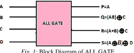
The 4*4 reversible ALL Gate [5] performs all the Basic Logical Operations like AND, OR, NOT, NAND, EXOR, EXNOR. It can be used for an ALU Design as it executes all the basic operations.
Fig. 1: Block Diagram of ALL GATE
The reversible ALL Gate is used to design all the logical operations as we have all the basic gates in the proposed ALL Gate. It is shown in the figure 1
KTR Gate as Full Adder
The Reversible KTR Gate [6] acts as Full adder to exhibit the Sum and Carry when the input D is Supplied as ‘0’ as shown in the figure 2. On Implementing KTR gate as a full adder we have 2 garbage outputs. Sum and Carry are taken in the output C and D respectively.
Fig. 2: Full adder using KTR Gate
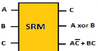
SRM Gate as Multiplexer
Http://www.ijetmr.com©International Journal of Engineering Technologies and Management Research [1-11]
Fig. 3: Block Diagram of the SRM Gate
Fredkin Gate
Fig 4 shows a 3*3 Fredkin gate. The input vector is I (A, B, C) and the output vector is O (P, Q, R). The output is defined by P=A, Q=A′B AC and R=A′C AB. Quantum cost of a Fredkin gate is 5. [13]
Fig. 4: Block Diagram of the Fredkin Gate
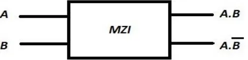
SOA Based MZI
A photon can provide unmatched high speed and can store the information in a signal of zero mass. These properties of photon have attracted the attention of researchers to implement the reversible logic gates in all optical domain. In the recent years, researchers have implemented several reversible logic gates in optical computing domain such as Feynman gate, Toffoli gate, Peres gate and Modified Fredkin gate. The all optical implementation of reversible logic gates can be achieved using semiconductor optical amplifier (SOA) based Mach-Zehnder interferometer (MZI) optical switches.
Http://www.ijetmr.com©International Journal of Engineering Technologies and Management Research [1-11]
Fig. 5: SOA Based MZ1
In MZI there are two inputs ports A and B and two output ports called as bar port and cross port respectively, as shown in Fig.6. At the input ports, the optical signal coming at port B is considered as the control signal (λ2) and the optical signal coming at port A is considered as incoming signal (λ1). The working of the MZI can be explained as: (i) when there is an incoming signal at port A and the control signal at port B then there is a light present at the output bar port and there is no light present at the output cross port, (ii) in the absence of control signal at input port B and incoming signal at input port A then the outputs of MZI are switched and results in the presence of light at the output cross port and no light at the bar port. In this work, consider no light or absence of light is considered as the value 0. The above behavior of MZI based all optical switch can be written as Boolean functions having inputs to outputs mapping as (A, B) to (P=AB, Q = AB ), where A (incoming signal), B (control signal) are the inputs of MZI and P (Bar Port), Q (Cross Port) are the outputs of MZI, respectively. The block diagram of MZI based all optical switch is shown in Fig.6. In this work the optical cost and the delay (Δ) of MZI based all optical switch is considered as unity.
Fig 6: Mach-Zehnder Interferometer
3. PROPOSED WORK
Introduction to the Garbage Less Gate (GLG)
The proposed GLG Gate is a 4 x 4 reversible gate. The inputs and the outputs be A, B, C, D and P, Q, R, S respectively.
Http://www.ijetmr.com©International Journal of Engineering Technologies and Management Research [1-11]
The proposed reversible GLG (Garbage Less Gate) Gate is used to design reversible 2:22 Decoder. 2:22 are implemented using a single GLG Gate.
Truth Table of GLG
From the truth table it is clearly inferred that the proposed GLG is perfectly reversible as it is one to one mapping. The truth table is provided in table 1.
Table 1: Truth Table of the proposed Gate
.
Decoder
A decoder is a combinational circuit used in many devices for processing [8]. It has multiple inputs as well as multiple outputs. Generally decoder is available as 2 to 4 decoder, 3 to 8 decoder, 4 to 16 decoder etc. A single Feynman gate can be used to design the basic 1 to 2 decoder.
2:4 Decoder using the proposed GLG
By using single GLG (Garbage Less Gate) the 2:4 Decoder were designed. Inputs A and B is given according to the block diagram and the input C and D is zero, the outputs are taken from
INPUT OUTPUT
A B C D P Q R S
0 0 0 0 1 0 0 0
0 0 0 1 0 1 1 0
0 0 1 0 1 0 0 1
0 0 1 1 0 1 1 1
0 1 0 0 0 1 0 0
0 1 0 1 1 0 1 0
0 1 1 0 0 1 0 1
0 1 1 1 1 0 1 1
1 0 0 0 0 0 1 0
1 0 0 1 1 1 0 0
1 0 1 0 0 0 1 1
1 0 1 1 1 1 0 1
1 1 0 0 0 0 0 1
1 1 0 1 1 1 1 1
1 1 1 0 0 0 0 0
Http://www.ijetmr.com©International Journal of Engineering Technologies and Management Research [1-11]
the P Q R and S output. Representation of the 2:4 Decoder. Using GLG Gate is given in the figure 8.
Fig. 8: Decoder Using GLG
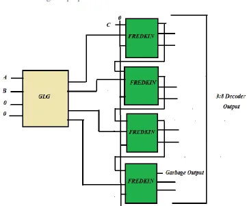
3 : 8 Decoder using the proposed GLG
Http://www.ijetmr.com©International Journal of Engineering Technologies and Management Research [1-11]
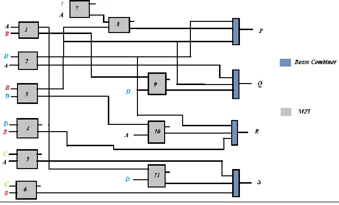
Optical Implementation of the proposed GLG
Fig. 10: Optical Implementation of the proposed GLG
Here we are using one GLG Gate and 4 Fredkin Gate to construct a 3:8 Decoder. It is very important to note that NOT Gate is the only one conventional logic gate which is Reversible as it possess one to one Mapping. As usual two inputs C and D is given as zero. The Inputs are given as A and B for GLG Gate. Then third Input is given in the second stage of the circuit. We can receive the output from the fredkin gate directly. The representation of the 3:8 decoder is shown in the figure 9.
Truth Table of the 3 : 8 Decoder
The truth table of the proposed 3:8 Decoder, when the last input of the fredkin Gate is supplied as zero is given below.
Table 2: Truth Table of 3: 8 Decoder (S=0)
INPUTS OUTPUTS
A B E Z7 Z6 Z5 Z4 Z3 Z2 Z1 Z0
0 0 0 0 0 0 0 0 0 0 1
0 0 1 0 0 0 0 0 0 1 0
0 1 0 0 0 0 0 0 1 0 0
0 1 1 0 0 0 0 1 0 0 0
1 0 0 0 0 0 1 0 0 0 0
1 1 0 0 0 1 0 0 0 0 0
1 1 0 0 1 0 0 0 0 0 0
Http://www.ijetmr.com©International Journal of Engineering Technologies and Management Research [1-11]
Table 3: Truth Table of 3: 8 Decoder (S=1)
The truth table of the proposed 3:8 Decoder, when the last input of the fredkin Gate is supplied as one is given above.
4. SIMULATION RESULT
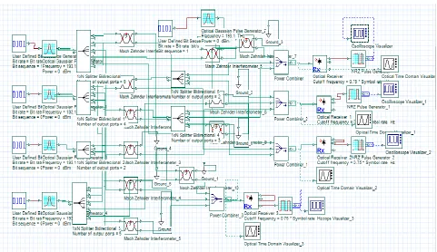
The circuit is also simulated using the Optisystem software. The optical implementation of the circuit is simulated and the output is verified.
When A=0 B=0 (Constant Inputs C=0 & D=0) the A bar B bar gets Selected (P=1)
INPUTS OUTPUTS
A B E Z7 Z6 Z5 Z4 Z3 Z2 Z1 Z0
0 0 0 0 1 1 1 1 1 1 1
0 0 1 1 0 1 1 1 1 1 1
0 1 0 1 1 0 1 1 1 1 1
0 1 1 1 1 1 0 1 1 1 1
1 0 0 1 1 1 1 0 1 1 1
1 1 0 1 1 1 1 1 0 1 1
1 1 0 1 1 1 1 1 1 0 1
Http://www.ijetmr.com©International Journal of Engineering Technologies and Management Research [1-11]
Similarly other outputs are verified.
The 2:4 Decoder is also simulated using the Modalism Software through the Verilog Code.
Http://www.ijetmr.com©International Journal of Engineering Technologies and Management Research [1-11]
5. COMPARISON
The reason why we say the proposed Decoder is an efficient one as it has no Garbage Output only one Gate is used to execute the decoder. The proposed 2:4 decoder using GLG Gate is very efficient as shown in the chart 1.
Chart 1: The proposed 2:4 decoder using GLG Gate
The proposed 3:8 decoder using GLG Gate and the NOT Gate is compared with the existing one [11], [12].
Chart 2: The proposed 3:8 decoder using GLG Gate and NOT Gate.
Also we can construct N: 2N Decoder using the proposed GLG Gate and the Fredkin Gate. 0 1 2 3 4 5 6 7
Gate Count Constant IP Garbage OP
Efficient 2 : 4 Decoder
Existing 9 Existing 10 Existing 11 Existing 12 Proposed One 0 2 4 6 8 10 12 14
Constant IP Garbage OP Gate Count Efficient 3 : 8 Decoder
Http://www.ijetmr.com©International Journal of Engineering Technologies and Management Research [1-11]
6. CONCLUSION
The drawback of any reversible digital circuit is high number of its gate count and the garbage output. This problem was overcome by the proposed design as it possesses only one gate and No Garbage Output. It is concluded that the proposed design is more efficient than the existing one.
7. REFERENCES
[1] A.Barenco, C.H. Bennett, R. Cleve, D.P. DiVincenzo, N. Margolus, P. Shor, T. Sleator, lA. Smolin, H. Weinfurter,"Elementary gates for quantum computation", Phys. Rev. A 52 (5) (1995) 3457-3467.
[2] Phillip Kaye, Raymond Laflamme, Michele Mosca "An Introduction to Quantum Computing" Oxford University Press Jan 2007eBook-LinG, ISBN 0-19-857000-7
[3] T.Toffoli, "Reversible computing", Tech memo MIT/LCS /TM-151, MIT Lab for Computer Science (1980).
[4] E. Fredkin and T. Toffoli, "Conservative logic", Int. 1. Theo. Phys., 21 (1982) 219.
[5]Theresal T ,Sathish K and Aswinkumar R, “ An Optimized Implementation of all Reversible Logic Gates using newly designed ALL GATE”, published at “ International Journal of Science and Innovative Engineering and Technology, Volume 2, May Issue 2015 Edition”.
[6] Sathish K, Aswinkumar R, Theresal T, Maivezhi Raja L, “A Low Power Reversible Braun Array Multiplier Architecture using KTR Gate” –Published at “International Journal of Emerging Trends in Engineering and Development, Volume 4, Issue 5, June-July 2015 Edition”. [7]Sathish K, Aswinkumar R, Theresal T, Bala Murugan T, “A Reversible Logic based Power Efficient N*1 Multiplexer Design using SRM Gate” –Published at “International Journal of Science, Engineering and Technology Research (IJSETR), Volume 4, Issue 6, June 2015 ”. [8] M. Morris Mano, Computer System Architecture, Pearson.
[9] M. Shamsujjoha, and H. M. H. Babu, ”A Low Power Fault Tolerant Reversible Decoder Using MOS Transistor,” 2013 26th International Conference on VLSI Design and the 12th International Conference on Embedded Systems, pp. 368 – 373, 2013.
[10] S. K. Noor Mahammad, S. K. Sastry Hari, S. Shroff, and VKamakoti, “Constructing online testable circuits using reversible logic”, Proceedings of the 10th IEEE VLSI Design and Test Symposium (VDAT), Goa, India, August 2006, pp. 373-383.
[11] R. Aradhya, R, Chinmaye, and K. Muralidhara, “Design, Optimizationand Synthesis of Efficient Reversible Logic Binary Decoder,”International Journal of Com-puter Applications, vol. 46, pp. 45-51,2012.
[12] Poodari Sairam Goud, Naveen Kumar, Reversible Applications of Decoder and Its Applications, International Journal & Magazine of Engineering, Technology, Management and Research Volume No: 1(2014), Issue No: 12 December 2014 Page 251.
[13]. http://web.cecs.pdx.edu/~mperkows/CLASS_VHDL_99/tran888/lecture003-reversible-logic.pdf.