Understanding PCIe performance for end host
networking
Rolf Neugebauer
Independent Researcher
Gianni Antichi
Queen Mary, University of London
José Fernando Zazo
Naudit HPCN
Yury Audzevich
University of Cambridge
Sergio López-Buedo
Universidad Autónoma de Madrid
Andrew W. Moore
University of Cambridge
ABSTRACT
In recent years, spurred on by the development and avail-ability of programmable NICs, end hosts have increasingly become the enforcement point for core network functions such as load balancing, congestion control, and application specific network offloads. However, implementing custom designs on programmable NICs is not easy: many potential bottlenecks can impact performance.
This paper focuses on the performance implication of PCIe, the de-facto I/O interconnect in contemporary servers, when interacting with the host architecture and device drivers. We present a theoretical model for PCIe andpcie-bench, an open-source suite, that allows developers to gain an accu-rate and deep understanding of the PCIe substaccu-rate. Using
pcie-bench, we characterize the PCIe subsystem in modern servers. We highlight surprising differences in PCIe imple-mentations, evaluate the undesirable impact of PCIe features such as IOMMUs, and show the practical limits for common network cards operating at 40Gb/s and beyond. Furthermore, throughpcie-benchwe gained insights which guided soft-ware and future hardsoft-ware architectures for both commercial and research oriented network cards and DMA engines.
CCS CONCEPTS
•Networks →Network adapters;Network servers; • Hardware→Networking hardware;Buses and high-speed links;
KEYWORDS
PCIe, reconfigurable hardware, Operating System
1
INTRODUCTION
The idea of end hosts participating in the implementation of network functionality has been extensively explored in enter-prise and datacenter networks [6, 7, 25, 49, 56, 58]. Moreover, the disruptive introduction into the market of programmable NICs, alongside the deployment in datacenters of hybrid Xeon and FPGA platforms [15], has boosted the demand for new refined solutions which combine software functions and
hardware NIC acceleration to improve end host network-ing performance [53], flexibility [16], or a combination of both [29]. Several efforts try to leverage end host hardware programmability to improve datacenter scalability [12, 13] or specific network functions such as load balancing, appli-cation level quality of service and congestion control [1].
In this paper, we show that PCIe, alongside its interaction with the host architecture and device drivers, can signifi-cantly impact the performance of network applications. Past research has mostly considered this impact in the context of specific applications such as Remote DMA (RDMA) [24], GPU-accelerated packet processing [17], and optimized Key-Value-Store (KVS) applications [31, 32, 34]. In contrast, we argue that a more generic approach to studying and char-acterizing PCIe is needed as it has become essential to im-plement not only specialized, high-performance network functions, but also storage adaptors and custom accelera-tor cards, such as for machine learning [23]. It is in this context that we introduce a theoretical model for PCIe (§3), design a methodology to characterize PCIe in real systems (§4), describe its implementation (§5), and present the results derived using our approach (§6). This permits us to draw several specific conclusions about the way PCIe currently operates and the implications this has for operating system and application design (§7). For example, we demonstrate how both NUMA for PCIe devices and IOMMUs can have a negative performance impact on application performance.
The contributions of this paper are:
• We introduce a model of PCIe. The model provides a baseline for expected PCIe throughput for a wide range of PCIe configurations. It also allows to quickly assess the performance impact when iterating through design alternatives for device and device driver interactions, e.g., when implementing custom NIC functionality.
• We outline a methodology,pcie-bench: a combination of micro-benchmarks that systematically measures aspects of performance for both a device’s DMA engines and, more crucially, the PCIe root complex1.
1The PCIe root complex connects the processors and memory subsystem of a host system with the PCIe switch fabric to individual PCIe devices. Its functionality is similar to the PCI host bridge in older systems.
• We describe two implementations ofpcie-benchbased on commodity PCIe peripherals: commercially available programmable NICs from Netronome and the latest NetF-PGA boards. The implementations are available as open source2to allow for the reproducibility of our results and to enable other practitioners to apply to other systems and architectures.
• We present the first, publicly-disclosed, detailed measure-ments of PCIe performance across several generations of conventional host-systems; this permits us to trace the evolution of PCIe root complex implementations and highlight some surprising differences between implemen-tations even from the same vendor.
• We discuss the lessons we learned alongside a number of practical use-cases forpcie-bench. From the original need to characterize, debug, and improve implementa-tions, to aid and evaluate the growing area of research of customized solutions enabled by programmable NICs. Furthermore, the results are also directly applicable to the growing number of other high-performance such as specialized accelerator cards.
2
MOTIVATION
Traditionally, I/O interconnects in commodity systems, such as PCIe, are not widely studied, in part, because they have worked effectively for many years. It is only as we have I/O devices that approach (and exceed) the capabilities offered by PCIe, e.g., dual-port 40Gb/s network adapters, that we have seen a significant number of hardware-software co-designs3
with the constraints of PCIe in mind [16, 29, 30]. Along-side them, many novel software frameworks have also been proposed to avoid the overhead of conventional network stacks [3, 8, 46, 54].
Unfortunately, with 40 and 100Gb/s NICs, PCIe, even in combination with optimized software stacks, is becoming the bottleneck. Moreover, modern network applications with tight latency requirements can be affected by the delays in-troduced by both the DMA engines in PCIe devices and the PCIe end-host implementation. Finally, the host-side imple-mentation of PCIe in modern x86 based servers has been changing dramatically, and alternative server architectures are also emerging. We now look at these aspects in more detail.
PCIe impact on network application throughput.A PCIe Gen 3 x8 interface, typically used by 40Gb/s NICs, has a throughput of 62.96 Gb/s at the physical layer. However, PCIe protocol overheads reduce the usable bandwidth to
2https://www.pcie-bench.org
3Such I/O-aware software design is hardly new. In the past, when faster ATM and 1Gb/s PCI bus adapters were introduced, many driver and kernel redesigns have been proposed [9, 50, 60].
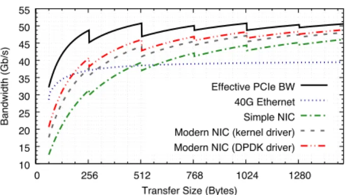
10 15 20 25 30 35 40 45 50 55 0 256 512 768 1024 1280 Bandwidth (Gb/s)
Transfer Size (Bytes)
Effective PCIe BW 40G Ethernet Simple NIC Modern NIC (kernel driver) Modern NIC (DPDK driver)
Figure 1: Modeled bidirectional bandwidth of a PCIe Gen 3 x8 link, the achievable throughout of a simplis-tic NIC and a modern NIC with a typical kernel driver and a DPDK driver.
around 50 Gb/s, or significantly less, depending on the PCIe access patterns. Figure 1 shows the effective bi-directional bandwidth achievable for such a device (Effective PCIe BW). The saw-tooth pattern is caused by thepacketized struc-ture of the PCIe protocol where the data to be transferred, e.g., a network packet, is broken up into smaller PCIe packets with their own PCIe level headers.
Apart from transferring the packet data itself, a NIC also has to read TX and freelist descriptors, write back RX (and sometimes TX) descriptors and generate interrupts. Device drivers also have to read and update queue pointers on the device. All these interactions are PCIe transactions consum-ing additional PCIe bandwidth. If we model a very simple NIC, which DMAs individual descriptors for every packet and where the driver reads/writes the queue pointers for every packet, we can see a dramatic decrease in achievable bi-directional bandwidth (Simple NIC). Such a device would only achieve 40 Gb/s line rate throughput for Ethernet frames larger than 512B. Most modern NICs (and drivers) therefore implement a number of optimizations, such as en-queuing descriptors in batches, pre-fetching descriptors, interrupt moderation, etc. These optimizations increase the complex-ity of the NIC but are required to achieve acceptable through-put.Modern NIC (kernel driver)in the figure shows the throughput of such a moderately optimized NIC/driver com-bination with a typical Linux kernel driver. Modern software frameworks, such as DPDK [8], enable further optimizations at the driver level (no NIC hardware changes). By disabling interrupts and polling write-back descriptors in host memory instead of device registers, the number of PCIe transactions is further reduced and the achievable bandwidth is increased (Modern NIC (DPDK driver)). We detail how these models are derived in Section 3. However, Figure 1 shows that when designing custom offloads to programmable NICs, developers
and researchers have to be acutely aware of the overheads imposed by PCIe transactions, caused both by the device and the device driver.
PCIe impact on network application latency.We used an ExaNIC [11] to estimate the contribution of PCIe to the overall end-host latency experienced by a network applica-tion. We executed a loopback test to measure the total NIC latency (from application to the wire and back) with various sized packets. The test writes a packet to the driver’s buffer and measures the latency between when the packet starts to be written to PCIe and when the packet returns. The test utilizes kernel bypass mode, so does not include any kernel overheads. We also modified the ExaNIC firmware, using Exablaze firmware development kit4, to measure the PCIe latency contribution. 600 800 1000 1200 1400 1600 1800 2000 2200 2400 0 200 400 600 800 1000 1200 1400 1600 90.6% 84.4% 77.2% Median Latency (ns)
Transfer Size (Bytes) NIC
PCIe contribution
Figure 2: Measurement of NIC PCIe latency. Figure 2 shows the results from the test. On the ExaNIC, the PCIe subsystem contributes between 77% of the latency for 1500B packets, increasing to more than 90% for small packet sizes. In particular, the overall latency is well within the range which has been shown to have negative impact on performance for several common datacenter applications [63]. Measurement of NIC PCIe latencyFigure 2 illustrates that the round trip latency for a 128B payload is around 1000nswith PCIe contributing around 900ns. With 40 Gb/s Ethernet at line rate for 128B packets, a new packet needs to be received and sent around every 30ns. Assuming that the measured PCIe latency is symmetric, this implies that the NIC has to handle at least 30 concurrent DMAs in each direction to accommodate this latency in order to achieve line rate for 128Bpackets. Given that a NIC also has to issue DMAs for descriptors, the number of in-flight DMAs a NIC has to handle is even higher. Furthermore, as we show in §6.2, some systems introduce significant variance in latencies, which the NIC’s DMA engines also have to accommodate. This not only introduces significant complexity when writing optimized software for programmable NICs but also imposes
4http://www.exablaze.com/docs/exanic/user-guide/fdk/fdk/
constraints on the device driver having to supply host buffers in large enough batches for the NIC to consume.
PCIe root complex is evolving. In modern, x86 based servers, the PCIe root complex has seen a rapid evolution in recent years. Specifically, together with the memory con-troller(s), it has been closely integrated with the CPU cores, enabling tighter integration of PCIe devices with a CPU’s caches, e.g., Intel’s Data Direct I/O (DDIO) [20]. For multi-socket systems, this integration also results in non-uniform memory access (NUMA [28]) for PCIe devices: Some DMA re-quests may target memory local to the socket the PCIe device is attached to while others need to traverse the CPU inter-connect. Finally, most modern systems have an IOMMU [22] interposed in the data path between a PCIe device and the host. The IOMMU performs address-translation for addresses present in PCIe transactions and utilizes an internal Trans-action Lookaside Buffer (TLB) as a cache for translated ad-dresses. On a TLB miss, the IOMMU must perform a full page table walk, which may delay the transaction and thus may increase latency and impact throughput. These recent technologies not only impact the overall latency (and band-width) of PCIe transactions, but they also introduce variance as transactions are now depending on the temporal state of caches, IOMMU TLB and the characteristics of the CPU in-terconnects. Furthermore, after years of a relative x86 mono-culture in the server market, designs around ARM64 and Power processors have all received mainstream deployment. Each of these architectures have vastly different implementa-tions of the I/O subsystem and most of the associated details are not publicly available, making it hard for researchers to characterize and understand the differences among these server architectures.
The impact of PCIe on the throughput experienced when data needs to be transferred from hardware to software and vice versa, the predominant contribution of PCIe to the over-all NIC latency, the introduction of new technologies in the PCIe root complex, and the mainstream deployment of new server architectures have motivated us to buildpcie-bench: to get a better, more detailed and systematic understand-ing of the PCIe implementation in commodity systems and to help developers to fine tune applications to make more efficient use of the underlying system.
3
MODELLING PCIE
As part ofpcie-benchwe have developed a model of the PCIe specification [47, 57]. The model allows us to: (1) vali-date bandwidth measurements from micro-benchmarks against expected bandwidth based on the specification, and (2) model the impact of more complex device/host interactions, such as shown in Figure 1 with the NIC models.
PCIe uses a high-speed serial interconnect based on a point-to-point topology consisting of several serial links (or lanes) between endpoints. It is a protocol with three lay-ers: physical, data link and transaction. While the data link layer (DLL) implements error correction, flow control and acknowledgments, the transaction layer turns user applica-tion data, or compleapplica-tion data, into PCIe transacapplica-tions using Transaction Layer Packets (TLPs).
Most available 40Gb/s NICs today have a PCIe Gen 3 in-terface with 8 lanes. Each lane offers 8 GT/s (Giga Trans-actions per second) using a 128b/130b encoding, resulting in 8×7.87Gb/s = 62.96Gb/s at the physical layer. The DLL adds around 8–10% of overheads due to flow control and acknowledgment messages, leaving around 57.88Gb/s
available at the TLP layer5. For each transaction, the physical layer adds 2Bof framing and the DLL adds a 6Bheader.
At the transport layer, the standard defines a number of different TLP types. For the purpose of this paper, the rele-vant packet types are: Memory Read (MRd), Memory Write (MWr), and Completion with Data (CplD). TLPs have a com-mon header, a type specific header, and an optional trailing digest. The common header contains information, such as the type of TLP and the TLP length, and is 4Bin size. The header of MWr and MRd TLPs is 12Blong (assuming 64bit addressing) while for CplD TLPs it is 8B. The maximum amount of data carried in a single TLP (Maximum Payload Size, or MPS) is negotiated between the peers and the op-tional 4Bdigest contains an end-to-end CRC (ECRC). Typical values for the MPS are 256Bor 512B.
PCIe MWr transactions are simplepostedtransactions and the number of bytes transferred by a DMA write of sizesz
can be calculated with:
Bt x=⌈sz/MPS⌉ ×MW r_Hdr+sz (1)
whereMW r_Hdr is 24B (2B framing, 6B DLL header, 4B
TLP header, and 12BMWr header). In contrast, PCIe mem-ory reads (MRd), e.g., a device reading data from the host, require two TLP types: MRd TLPs and CplD TLPs. A MRd TLP is sent to request data from the peer, then the data is returned via one or more CplD TLPs. Thus, PCIe memory reads consume bandwidth in both directions. A MRd request may only request data up a certain amount (Maximum Read Request Size, or MRRS), negotiated between the peers. A typical value for the MRRS is 512B. The data returned via CplD TLPs is bounded by the MPS. The number of bytes consumed for a DMA read of sizeszis then:
Bt x =⌈sz/MRRS⌉ ×MRd_Hdr+sz (2)
Br x =⌈sz/MPS⌉ ×CplD_Hdr+sz (3)
5The DLL overhead depends on the transaction rate and implementation details. The value of 57.88 Gb/s was derived using recommended values from the PCIe specification [47].
withMRd_Hdr being 24BandCPL_Hdr20B.
The PCIe configuration of a device, e.g., PCIe Gen 3 device with 8 lanes (x8), provides us with the available bandwidth and the values for MPS and MRRS. With the formula above, we can then calculate the effective bandwidth for different transfer sizessz. The graphEffective PCIe BWin Figure 1 was calculated using this model assuming a PCIe Gen 3 x8 de-vice,MPS=256B, andMRRS=512Busing 64bit addressing. The saw-tooth pattern shows the overhead of the additional DLL/TLP headers for every MPS bytes of data, with the over-head being higher for smaller transfer sizes. The graph also shows the impact of MRRS as the additional MRd TLPs con-sume bandwidth which otherwise would be usable by MWr transactions.
The model also allows us to calculate the overhead for more complex device/host interactions. For example, for the graph of theSimple NICin Figure 1 we calculate the PCIe bandwidth used both for packet send (TX) and receive (RX) of a simple NIC. For TX, the driver writes updates the TX queue tail pointer on the device (4BPCIe write). The device then DMAs the descriptor (16BPCIe read) and, subsequently, the packet buffer. After transmission, the device generates an interrupt (4BPCIe write) and the driver reads the TX queue head pointer (4BPCIe read). For RX, the driver updates the RX queue tail pointer to enqueue a buffer on the freelist (4B
PCIe write). The device then DMAs the freelist descriptor (16BPCIe read), DMAs the packet (PCIe write) and the RX descriptor (16B PCIe write) to the host and generates an interrupt (4BPCIe write). Finally, the driver reads the RX queue head pointer (4BPCIe read). The model then calculates the overhead for each of these transactions and computes the achievable bandwidth.
The NIC model described above is very simplistic and all modern NICs deploy a variety of optimizations. For example, the Intel Niantic NIC [19] DMAs batches of up to 40 TX descriptors from the host and may write batches up to 8 TX descriptors back to the host.Optimized NIC (kernel driver)in Figure 1 shows the performance impact of these optimizations over the simple NIC model. Throughput can be further improved by driver changes, as shown byOptimized NIC (DPDK driver)in the same figure. The Intel DPDK driver configures the device differently: no interrupts are generated and the driver does not read device registers to determine if packets have been received/transmitted6. The
graphs for the optimized NIC show that even a moderate amount of optimization on both the device and the driver side can significantly improve the achievable throughput.
6The DPDK driver polls on descriptor queues in host memory instead, checking for the valid fields indicating that a descriptor has been updated. 4
Our PCIe model is not limited to calculating achievable throughput for NICs. It can equally be used to programmat-ically modelany PCIe device, provided that some details, typically obtainable from the device driver or the data sheet, are available. Furthermore, the model can and has been used to quickly assess the impact of alternatives when designing custom NIC functionality. The model has some limitations: Some of the lower level PCIe overheads, in particular for flow control messages are only estimated based on the PCIe spec-ification and the model slightly overestimates their impact. Furthermore, the model does not account for PCIe overheads of unaligned DMA reads. For these, the specification requires the first CplD to align the remaining CplDs to an advertised Read Completion Boundary (RCB, typically 64B) and un-aligned PCIe reads may generate additional TLPs.
4
THE
PCIE-BENCH
METHODOLOGY
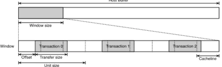
While the PCIe protocol stack is relatively easy to model, it is the implementation of the DMA engine and, in particular, the increased complexity of the PCIe root complex, discussed in §2, which makes it hard to evaluate the end to end PCIe performance in real systems. Therefore, we designed a set of PCIe micro-benchmarks in the spirit oflmbench[39] and hbench:OS[5]. The main idea is to perform individual PCIe operations from a device to a buffer in host memory while carefully controlling the parameters which may affect per-formance. Transaction 0 Transaction 1 Host Buffer Window size Cacheline Window
Offset Transfer size Unit size
Transaction 2
Figure 3:Host buffer layout and access parameters
Figure 3 illustrates the host buffer setup and the param-eters which determine the access from a PCIe device. We define a (logically) contiguous buffer on the host. The buffer may be contiguous in DMA address space or comprised of a number of smaller buffers. It must be significantly larger than the size of the Last Level Cache (LLC), because, on some ar-chitectures, the PCIe root complex interfaces with the cache system of the CPUs. To measure cache effects, only a subset of the host buffer, thewindow size, is accessed repeatedly.
For a given micro-benchmark we access the window size of the host buffer with multiple DMA requests and keep the amount of data transferred with each request fixed (transfer size). A DMA may start at anoffsetfrom a host cache line,
allowing us to determine if there are any penalties for un-aligned accesses. To ensure that each DMA request touches the same number of cache lines, the window is divided into equal sized units. Each unit is the sum of offset and transfer size, rounded up to the next cache line. A micro-benchmark can typically be configured to access the units sequentially or randomly (access pattern), though for most experiments in this paper we use random access. For each benchmark, thestate of the CPU cacheneeds to be carefully controlled. By default, the cache is thrashed before every benchmark to ensure acoldcache. Optionally, we may attempt to warm the cache from the host, by writing to the window (host warm), or from the device. The latter is achieved by issuing a number of write DMAs to the window (device warm), before running tests. Understanding the impact of the host cache system is important: when transmitting packets from the host, typically, at least the packet header would be cache res-ident, and when receiving from the network, the packet data may get DMAed to non-cache resident buffers, depending on the overall pressure on the caches. Finally, thelocality of the host buffer needs to be controlled. In SMP systems with integrated PCIe and memory controller, the entire host buffer is either allocated local to the node the PCIe device is attached to, or to a different (non-local) node.
4.1
Latency benchmarks
The first set of the PCIe micro-benchmarks measures the latency of individual PCIe operations. Measuring the latency of a PCIe Memory Read (MRd) transactions (from the device) is relatively easy on most programmable hardware: take a timestamp before issuing a DMA Read and another times-tamp when the completion of the DMA Read is signaled by the DMA engine, then log the time-difference. DMA Read latency benchmarks are labeledLAT_RDthroughout.
The latency of DMA Memory Writes can not be mea-sured directly from the device as PCIe Memory Write (MWr) transactions areposted: they are sent without explicit ac-knowledgment of success. Instead, we indirectly measure the latency of writes by issuing a DMA Write followed by a DMA Read from the same address. PCIe ordering ensures that the PCIe root complex handles the Read after the Write. Note, this approach does not allow us to compute the latency of DMA Writes alone as the latency of the DMA Read may be affected by the preceding DMA Write. The results from these benchmarks are labeledLAT_WRRD. For latency benchmarks we record the latency for each transaction and then calculate the average, median, min, max, 95th, and 99th percentile.
Latency measurements allow us to assess the cost of cache and IO-TLB misses, or the added latency for accessing re-mote memory from a PCIe device. While we can not measure the latency of a DMA Write directly, the latency of a DMA
Write followed by a DMA Read to the same address pro-vides insights into technologies, such as DDIO. Measuring latency includes the device overheads, such as the cost of issuing DMA requests or receiving notifications of comple-tions. Therefore, when looking at the impact of the PCIe root complex, it is more insightful to study the relative change in latencies rather than the absolute latency values.
As highlighted in Section 2, latency measurements are of particular importance when writing software for pro-grammable NICs or when implementing DMA engines in (reconfigurable) logic: the measured latency in Figure 2 by far exceeds the inter-packet times for small packets. Mea-sured latency and its variance determines how many in-flight DMAs need to be handled.
4.2
Bandwidth benchmarks
The second set of PCIe micro-benchmarks focuses on band-width. DMA bandwidth is measured by taking a timestamp at the start, issuing a significant number of DMAs and taking a timestamp at the end. The bandwidth can be calculated by the time difference and the amount of data transferred. We are interested in straight DMA Read and DMA Write band-width (labeledBW_RDandBW_WRrespectively). To measure bi-directional bandwidth we issue alternating DMA Read and Write transactions (labeledBW_RDWR). This ensures that PCIe MRd TLPs compete with PCIe MWr TLPs for the bandwidth to the root complex.
Bandwidth benchmarks, especially with small transfer sizes and random access patterns, generate a significant load on the system. If the DMA engine can saturate the PCIe link with 64 byte transfers, this would generate around 69.5 million transactions per second in each direction with the root complex handling a transaction every 5ns. Therefore, bandwidth micro-benchmarks can expose limitations in the root complex implementation as well as stressing the imple-mentation of a device’s DMA engines.
5
IMPLEMENTATIONS
Thepcie-benchmethodology requires programmatic and fine grained control over the PCIe device’s DMA engines. We have implemented the methodology on both commer-cial boards from Netronome and research oriented NetF-PGA boards. Two independent implementations of the same methodology validate our performance measurements against different host architectures and provide direct insights into two different PCIe implementations.
5.1
Netronome NFP implementations
Netronome offers a number of highly programmable NICs based on the NFP-6000 and NFP-4000 Ethernet controllers [44, 45, 59]. These Ethernet controllers feature up to 120eight-way multi-threaded Flow Processing Cores (FPCs), a hierarchical memory subsystem, and fully programmable PCIe interfaces, all interconnected via a distributed switch fabric. The PCIe subsystem exposes two interfaces to the FPCs: Acommandinterface allowing the core to issue small PCIe read and write transactions directly from registers and a bulkDMAinterface allowing FPCs to en-queue large trans-fers between host memory and memory on the NFP. The PCIe micro-benchmarks are implemented as firmware on the FPCs utilizing both interfaces. The micro-benchmarks work both on NFP-4000 and NFP-6000 based controllers. Firmware.The full PCIe micro-benchmark suite is imple-mented in a single firmware image. It provides a simple control interface, allowing a user space program on the host to select which type of benchmark to run and provide the necessary configuration parameters, such as the host buffer location, transfer size etc. Benchmark results are written to NFP memory where they can be read back from the host.
Latency tests are run on a single thread in one of the FPCs. This thread calculates the next host address to use and pre-pares a DMA descriptor. The thread then reads the current value of the internal timestamp counter and enqueues the DMA descriptor to the DMA engine. The DMA engine sig-nals the thread once the DMA completed and the thread takes another timestamp and journals the difference to mem-ory on the NFP. A variant of the latency benchmarks uses the direct PCIe command interface, which is suitable for small transfer (up to 128 bytes). With this variant, instead of build-ing and enqueubuild-ing a DMA descriptor, the thread can directly issue the PCIe read or write commands and gets signaled on completion. The timestamp counter increments every 16 clock cycles, which, on a 1.2 GHz NFP, provides a resolution of 19.2ns. For latency benchmarks we typically journal the timing for 2 million transactions.
For DMA bandwidth tests, the challenge is to ensure that DMA descriptors are enqueued to the DMA engine at a higher rate than it drains the queue. To achieve this for small transfer sizes, we use 12 cores with 8 threads as DMA workers. In a loop, each DMA worker thread calculates a host address, prepares and enqueues a DMA descriptor and yields until the completion is signaled. An atomic counter, shared between all workers, is decremented before issuing a new DMA request. If the counter value goes below zero, the worker stops. ForBW_RDWRtests, each worker issues a DMA Read if the counter is even and a DMA Write when the counter is odd. A control thread is used to start all the worker threads and waits for them to complete. The elapsed time is used to calculate the achieved bandwidth. For band-width tests 8 million DMA requests are performed. For both DMA latency and bandwidth tests the DMA descriptors are configured to target an internal 256 KB SRAM, known as the
Cluster Target Memory. This memory has an access latency of 50-100 cycles. Enqueuing DMA descriptors incurs a sim-ilar latency. These latencies add a fixed cost to each DMA transfer, and while they are specific to the NFP, we expect other programmable NICs to have similar overheads. The firmware is implemented in Micro-C, an NFP specific exten-sion to C. The micro-benchmark suite is implemented with around 1500 lines of code, with the core requiring around 500 lines of code. The code can be compiled, without exter-nal dependencies, to run on NFP6000 and NFP4000 based networking cards.
5.2
NetFPGA
NetFPGA is an open-source community platform [43]. It is supported by cutting-edge reconfigurable boards, reference software and hardware designs, as well as the infrastructure for design development and verification. The latest gener-ation of NetFPGA board, NetFPGA-SUME, is a PCIe host adapter card [62] capable of 100Gb/s application speeds. The board utilizes a large Xilinx Virtex-7 FPGA device incorpo-rating two PCIe Gen 3hard-blocks, along with resources such as QDRII+ and DDR3 memory types.
Hardware.The PCIe micro-benchmark suite is implemented directly on the FPGA. It enhances the DMA engine described in [61] withpcie-benchcapabilities. The system provides a simple control interface, allowing the host to select which micro-benchmark to run along with its parameters. The sys-tem keeps track of time through a free-running counter, operating at PCIe core frequency (250MHz), providing a res-olution of 4ns. Every time the software triggers a new micro-benchmark, a finite state machine coded into the hardware, calculates the host addresses and generates the associated memory read or write request. The design does not use a FIFO to enqueue DMA requests, instead the DMA requests are directly passed to the DMA engine. All the memory requests are generated on-the-fly as the hardware design allows transmission of a new request every clock cycle.
For latency tests, the system is configured to take a times-tamp before a DMA read and after the acknowledgment signal is received. The system records up to 1000 latency values. For bandwidth tests, the system measures the total time it takes to perform 1 million transactions. Benchmark results are written to NetFPGA memory after a benchmark run, where they can be read back from the host. The FPGA design is written in Verilog and System Verilog. The micro-benchmark suite is implemented with around 1200 lines of code. It can be compiled for NetFPGA-SUME and Xilinx VC709 boards.
5.3
Kernel drivers
Both the NFP and the NetFPGA implementations use a kernel driver to initialize the hardware, allocate host memory for DMAs and provide access to user space programs to control the execution of the benchmarks and to collect the results. The NFPpcie-benchdriver uses the standard NFP kernel driver7. It allocates the host side DMA buffers in chunks of 4MB as this the maximum size which can be allocated physically contiguous on most Linux kernel versions. The NetFPGA driver allocates memory either fromhugetlbfs
(with 1GB pages) or standard 4KB system pages.hugetlbfs
is the default option as it allows for the easy allocation of large, physically contiguous areas of memory. Both drivers provide control over which NUMA node memory is allocated from and export an interface allowing a user space program to warm the caches with the controlled portions of the host DMA buffers. The NFPpcie-benchkernel module is im-plemented in around 400 lines of code while the NetFPGA driver is implemented in approximately 800 lines of code.
5.4
Control programs
The execution of benchmarks, gathering of the data and post-processing of the results is performed by user space programs in both implementations. The NFP implementation uses a Python program with a small utility, written in C, to handle cache warming. The Python program can be used to run individual tests or a full suite of tests. A complete run takes about 4 hours and executes around 2500 individual tests. For latency benchmarks, the control program reads the timing data of the individual transactions and calculates various metrics, such as the average, median, min, max and 95th and 99th percentile. Optionally, it generates CDFs, histograms and time series of the data. For bandwidth tests, the control program calculates the bandwidth and transaction rate. It is implemented in 1600 lines of Python and 120 lines of C code.
The NetFPGA control program is implemented in approx-imately 600 lines of C code and provides a command line interface to control the individual test parameters. The raw test results are written to a file for further processing.
5.5
Implementation on other devices
pcie-benchis best implemented on PCIe devices providing programmatic, fine-grained control over the DMA engines, such as the Netronome NFP and NetFPGA described above. There is a growing number of PCIe cards with similar capabil-ities. For example, the Intel Xeon Phi coprocessor exposes the device’s DMA engines via descriptor rings both to the Phi’s cores and the host [18]. There are also a growing number of programmable NICs with integrated FPGAs, such as the
7https://github.com/Netronome/nfp-drv-kmods 7
already mentioned Exablaze NICs [11] and Mellanox’s Pro-grammable ConnectX-3 Pro [40]. Implementingpcie-bench
on these devices should require roughly the same effort as it took for the initial two implementations.
Some limited aspects of pcie-benchcould potentially be implemented on non-programmable, commodity NICs in loopback mode by carefully controlling the locations of buffers used for packet send and receive. For example, one could repeatedly enqueue the same packet buffer for trans-mit and vary the freelist buffers to direct received packets to a variable window size (or vice versa). The relative changes in latency or bandwidth may provide some insight into host side PCIe implementation and changing the alignment of buffer addresses may reveal limitations of a device’s DMA engines. Note, however, the results will likely be less accurate than those obtainable with programmable PCIe devices as measurements with commodity NICs would always include overheads for descriptor transfers.
6
EXPERIMENTAL EVALUATION
This section reports thepcie-benchsuite in action. Table 1 lists the details of the systems used for the evaluation results presented in this paper. We focus on systems built around Intel’s Xeon E5 processors as this is the most common config-uration used in datacenter servers at the time of writing [55]. We discuss results obtained comparing several generations of Xeon E5 processors but also include some data from an Intel Xeon E3 system to compare results with a different pro-cessor architecture. For all experiments we use a PCIe Gen 3 x8 configuration as it is the default for modern NICs. We ex-pect thepcie-benchmethodology to be equally applicable to other PCIe configurations including the next generation PCIe Gen 4 once hardware is available.
6.1
Baseline bandwidth and latency
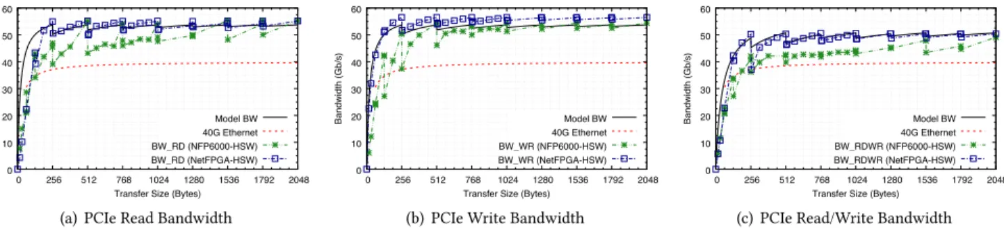
As the first set of results we present the baseline throughput of the NFP-6000 and NetFPGA implementations in Figure 4. We compare them to the required bandwidth for 40Gb/s Eth-ernet as well as a simplified model of achievable throughput for a PCIe Gen 3 device. The model accurately calculates the overhead of the physical, data link, and transaction layer of PCIe but onlyestimatesthe overhead of flow control mes-sages. We measure the throughput of PCIe read, write, and alternating read/write transfers for different transfer sizes to a fixed, 8KB host buffer, which is warmed before each test to eliminate any caching effects. We vary the transfer size from 64B to 2048B in rough increments of powers of 2 but take additional measurements with−1/+1B around important transfer sizes, such as some cache line or TLP size bound-aries. All DMA start addresses are cache line aligned and all tests were performed on the same Xeon E5 2637v3 system to
eliminate any differences in system configuration. Figure 4 shows the results.
In all three data sets, the NetFPGA implementation of
pcie-benchclosely follows the PCIe bandwidth calculated with our model. For PCIe writes the NetFPGA implementa-tion achieves a slightly higher throughput though. This is because the model assumes a fixed overhead for flow control messages which, for uni-directional traffic, would not impact traffic throughput. The NFP implementation ofpcie-bench
generally achieves slightly lower throughput than the NetF-PGA implementation (but typically achieves throughput suf-ficient to support 40Gb/s Ethernet rates). The main reason is that the NetFPGA implementation directly drives the DMA engines from the internal FPGA memory and does not per-form any additional processing. In the NFP implementation, the DMA engines must also transfer data to/from the host into internal SRAM, and then transfer it further into NFP internal memory where it can be accessed by the FPCs of the NFP card. These additional overheads, as well as the re-quired buffer management and signaling, introduce a slight performance degradation. Finally, it is worth noting that each graph shows that neither implementation is able to achieve a read throughput required to transfer 40Gb/s Ethernet at line rate for small packet sizes.
Next, we look at the latency of individual DMA transac-tions varying the transfer size (Figure 5). The setup is the same as for the bandwidth results described above. Overall, the latency numbers for both the NFP-6000 and NetFPGA are of the same order of magnitude, indicating that the bulk of the latency can be attributed to general PCIe and overall host overheads. It is very similar across the four generations of Intel processors we measured and is also in line with the latency measured using the ExaNIC presented in § 2.
The latency for DMA requests is higher on the NFP-6000 with an initial fixed offset of about 100nsfor smaller trans-fers, and the gap increasing for larger transfers. The reasons are twofold. The fixed offset can be explained with the over-head of enqueuing DMA descriptors to the DMA engines, which is avoided in the NetFPGA implementation. When using the NFP’s direct PCIe command interface, designed for smaller transfers, the NFP-6000 achieves the same latency as the NetFPGA, further indicating that the majority of the latency can be attributed to host system. The widening of the gap as the transfer size increases can be explained by consid-ering the internal architecture of the NFP (§ 5.1). Every DMA transfer to/from the host causes an additional transfer from the internal SRAM to NFP internal memory. This additional transfer increases the latency depending on the transfer size, but it is useful for decoupling the DMA request from the (variable) packet processing times performed by the FPCs.
Name CPU NUMA Architecture Memory OS/Kernel Network Adapter NFP6000-BDW Intel Xeon E5-2630v4 2.2GHz 2-way Broadwell 128GB Ubuntu 3.19.0-69 NFP6000 1.2GHz NetFPGA-HSW
Intel Xeon E5-2637v3 3.5GHz no Haswell 64GB Ubuntu 3.19.0-43 NetFPGA-SUME
NFP6000-HSW NFP6000 1.2GHz
NFP6000-HSW-E3 Intel Xeon E3-1226v3 3.3GHz no Haswell 16GB Ubuntu 4.4.0-31 NFP6000 1.2GHz NFP6000-IB Intel Xeon E5-2620v2 2.1GHz 2-way Ivy Bridge 32GB Ubuntu 3.19.0-30 NFP6000 1.2GHz NFP6000-SNB Intel Xeon E5-2630 2.3GHz no Sandy Bridge 16GB Ubuntu 3.19.0-30 NFP6000 1.2GHz
Table 1: System configurations. All systems have 15MB of LLC, exceptNFP6000-BDW, which has a 25MB LLC.
0 10 20 30 40 50 60 0 256 512 768 1024 1280 1536 1792 2048 Bandwidth (Gb/s)
Transfer Size (Bytes) Model BW 40G Ethernet BW_RD (NFP6000-HSW) BW_RD (NetFPGA-HSW)
(a) PCIe Read Bandwidth
0 10 20 30 40 50 60 0 256 512 768 1024 1280 1536 1792 2048 Bandwidth (Gb/s)
Transfer Size (Bytes) Model BW 40G Ethernet BW_WR (NFP6000-HSW) BW_WR (NetFPGA-HSW)
(b) PCIe Write Bandwidth
0 10 20 30 40 50 60 0 256 512 768 1024 1280 1536 1792 2048 Bandwidth (Gb/s)
Transfer Size (Bytes) Model BW 40G Ethernet BW_RDWR (NFP6000-HSW) BW_RDWR (NetFPGA-HSW)
(c) PCIe Read/Write Bandwidth
Figure 4: Baseline PCIe DMA bandwidth forNFP6000-HSWandNetFPGA-HSWwith warm caches.
400 600 800 1000 1200 1400 1600 8 16 32 64 128 256 512 1024 2048 Latency (ns)
Transfer Size (Bytes) LAT_RD (NFP6000-HSW) LAT_RD (NetFPGA-HSW) LAT_WRRD (NFP6000-HSW) LAT_WRRD (NetFPGA-HSW)
Figure 5:Median DMA latency for NFP-6000 and NetFPGA; minimum and 95th percentile are shown as error bars.
6.2
Comparing architectures
Figure 5 shows that the minimum and 95th percentile of DMA latencies for a Intel Xeon E5 system are very close to the median latency, suggesting that there is little variance in the latency experienced by PCIe transactions. Figure 6 shows the distribution of 64B DMA read latencies for the same system (NFP6000-NFP) as a CDF. The graph confirms that 99.9% of all transactions fall inside a narrow 80nsrange starting with a minimum of 520nsand a median of 547ns. The maximum latency out of 2 million transactions was 947ns.
The figure also shows the result from a Xeon E3 system of the same processor generation (NFP6000-HSW-E3). The results stand in stark contrast to those from the Xeon E5 system. The minimum latency on the Xeon E3 system is
0 0.2 0.4 0.6 0.8 1 0 1000 2000 3000 4000 5000 6000 CDF Latency (ns) NFP6000-HSW NFP6000-HSW-E3
Figure 6:Latency distribution for Xeon E5 and E3 for 64B DMA reads with warm caches.
actually lower with 493nsbut the median is more than double with 1213ns. Furthermore, from around the 63rd percentile the latency increases dramatically with the 90th percentile being double the median and the 99th percentile being 5707ns. The 99.9th percentile (11987ns) is an order of magnitude larger than the median with most latencies beyond being larger than 1msup to a maximum latency of 5.8ms.
The differences are also reflected in the bandwidth bench-marks (not shown) where for DMA reads the Xeon E3 system only matches the Xeon E5 system for transfers larger than 512B and, for DMA writes, never achieves the throughput required for 40Gb/s Ethernet for any transfer size.
We can only speculate on the causes for this different behavior. It seems likely that Intel maintains completely different PCIe root complex implementations for its Xeon E5 and Xeon E3 lines of processors. Looking in more detail at the
Xeon E3 data, there is no regular pattern to the occurrence of the longer latencies. We suspect that, in particular the larger latencies may be related to hidden power saving modes. We have previously observed large (<1ms) latencies on Xeon E5 systems before disabling power saving modes in the BIOS. However, disabling them on the Xeon E3 system did not significantly change the latency distribution.
6.3
Caching and DDIO
We now examine the impact of caching and DDIO on PCIe transactions. For these experiments we keep all parameters constant, except for the window size and the state of the LLC. The window size was varied from 4KB to 64MB, exceeding the 15MB or 25MB size of the LLC on all our systems.
Firstly, we look at PCIe transaction latency. To measure the latency we use the NFP’s PCIe command interface with 8 Byte transactions, as it is the lowest latency operation we have available. We ensure that each subsequent transaction touches a different cache line as described in Section 4.1. The results are shown in Figure 7(a). For PCIe reads (LAT_RD) with a cold cache we see no changes in latency as we change the window size: All PCIe reads are serviced from memory. When the cache is warm, the read latency is around 70ns
lower but increases once the window size exceeds the size of the LLC. This confirms that PCIe reads are serviced from the LLC if the data is resident in the cache. With a warm cache, the latency of a posted PCIe write followed by a read (LAT_WRRD) follows roughly the same pattern: writes and reads hit the LLC and, once the window size exceeds the LLC size, the latency increases by around 70ns. For a cold cache theLAT_WRRDresults illustrate the effect of DDIO: For small window sizes new cache lines get allocated and writes (and subsequent reads) are performed to/from the cache. Once the window size exceeds the 10% of the LLC reserved for DDIO, dirty cache lines have to be flushed out to memory before the write can succeed, causing a 70nsdelay for most writes. For larger transfer sizes, the differences between hitting the cache or not is reduced significantly: for 64BLAT_WRRDtests the difference is around 10ns.
The bandwidth data, presented in Figure 7(b), suggest a similar story. For 64B DMA Reads (BW_RD), there is a mea-surable benefit if the data is already resident in the LLC. For larger transfer sizes (not shown) the benefit is smaller, and from 512B DMA Reads onwards, there is no measurable dif-ference. For DMA Writes (BW_WR), there is no benefit if the data is resident in the cache or not. There is also no mea-surable benefit on keeping the windows size below the 10% of the LLC. We suspect that the DDIO portion of the cache is cleaned quick enough, so that all DMA Writes either hit the main LLC or the DDIO portion. Since DDIO can not be
disabled and there are no dedicated performance counters it is not possible to validate this hypothesis.
6.4
NUMA impact
With the PCIe root complex and memory controllers inte-grated in each CPU node, a PCIe device may access memory local or remote to the node to which it is attached. In this section we evaluate the performance impact of this non-uniform memory access. The host buffer is allocated either on the node the PCIe device is attached to (local) or on the other node in a 2-way NUMA system (remote). The cache is warmed or thrashed on the node the buffer is allocated from. Figure 8 shows the percentage change for DMA read band-width of local memory versus remote memory for different transfer sizes across different window sizes with a warm cache. 64B DMA reads experience a 20% drop in throughput (from∼32Gb/s to∼25Gb/s). The difference drops to around 10% once the DMAs are not serviced from the local cache anymore. With 128 and 256B DMA reads the penalty for accessing remote memory drops to 5-7% (e.g., from∼44Gb/s to∼41Gb/s for 128B). There is no noticeable penalty for 512B DMA reads. The data is confirmed by cold cache DMA read throughput (not shown) where remote 64B reads experience a constant 10% penalty (∼5% for 128B and 256B reads).
The throughput of DMA Writes does not seem to be af-fected by the locality of the host buffer nor by the size of the host buffer. In contrast with the Intel specification [20], we believe that all DMA Writes may be initially handled by the local DDIO cache.
For completeness, the latency numbers do not differ much from the local case presented in Figures 5 and 7 except that remote accesses add a constant 100nsof latency to our sys-tems. Overall, the results from our two dual socket systems (NFP6000_BDW and NFP6000_IB) are the same, indicating there has been little change in the two generations sepa-rating them.
6.5
The IOMMU effect
Finally, we look at the impact of an IOMMU interposed in the datapath between PCIe devices and the host. To mea-sure the impact of the IOMMU, we enable it on the Linux kernel command line withintel_iommu=on. IOMMU imple-mentations in Ivy Bridge and newer architectures support super-pages to reduce the number of page table entries, and thus reduce the number of TLB entries. For our experiments we disable this behavior (by also specifyingsp_offon the kernel command line). This forces the use of 4KB page table entries and allows us to use a relatively small 64MB host buffer for our experiments.
350 400 450 500 550 600 650 700 750 4K 16K 64K 256K 1024K 4096K 16384K 65536K Latency (ns)
Window size (Bytes) 8B LAT_RD (cold)
8B LAT_RD (warm)
8B LAT_WRRD (cold) 8B LAT_WRRD (warm)
(a) Median latency; minimum and 95th percentile are shown as error bars. 0 5 10 15 20 25 30 35 40 4K 16K 64K 256K 1024K 4096K 16384K 65536K Bandwidth (Gb/s)
Window size (Bytes) 64B BW_RD (cold)
64B BW_RD (warm)
64B BW_WR (cold) 64B BW_WR (warm)
(b) Bandwidth
Figure 7: Cache effects on Latency and Bandwidth (NFP6000-SNB)
-50 -40 -30 -20 -10 0 4K 16K 64K 256K 1024K 4096K 16384K 65536K % c hange of bandwidth
Window size (Bytes) 64B BW_RD 128B BW_RD
256B BW_RD 512B BW_RD
Figure 8:Difference between local and remote DMA Reads of different sizes with warm cache (NFP6000-BDW).
-70 -60 -50 -40 -30 -20 -10 0 4K 16K 64K 256K 1024K 4096K 16384K 65536K % c hange of bandwidth
Window size (Bytes) 64B BW_RD
128B BW_RD 256B BW_RD 512B BW_RD
Figure 9:Impact of IOMMUs on DMA reads of different transfer sizes with warm caches (NFP6000-BDW).
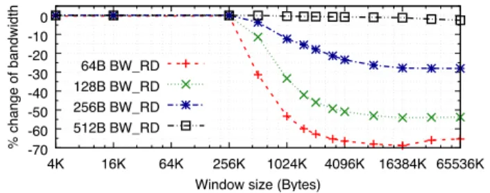
Figure 9 shows the result for different transfer sizes. Like the data presented in Section 6.4 the graph shows the per-centage change to the same experiment run without IOMMU. For small window sizes, there are no measurable differences across the range of transfer sizes. However, once the win-dow size is increased beyond 256KB, the throughput drops dramatically. For 64B DMA Reads it drops by almost 70% and even for 256B DMAs the drop is still a significant 30%. There is no change for transfer sizes of 512B and above. For DMA Writes (not shown), the drop is not quite as dramatic (55% for 64B writes), but is still very significant.
From this data we conclude that on that particular system the IO-TLB has 64 entries (256KB/4KB), a number that is not
published by Intel. The latency of 64B Reads increases from around 430nsto 760ns, putting the cost of an IO-TLB miss and subsequent page table walk at around 330ns. For smaller transfer sizes this penalty is relatively high compared to the time it takes to transfer the data, and thus the impact on the throughput is higher still. The data is surprisingly consistent across all 4 generations of Intel micro-architectures where we ran the experiments, and we observe the same effects with our NetFPGApcie-benchimplementation. With such consistent results across the 4 micro-architecture genera-tions we conclude Intel’s IOMMUs have undergone little development since their first implementation.
7
LESSON LEARNED AND USE CASES
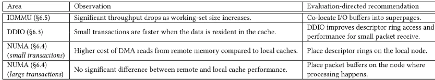
The results obtained frompcie-benchcan be and have been used to characterize and tune system software for high per-formance I/O. There are a plethora of sophisticated tools to analyze operating system and application performance, e.g., [14, 21], as well as tools to understand the performance impact of host CPU architectures and OS primitives, e.g., [5, 39]. However, none of these tools provide detailed insights into the performance of the I/O subsystem.pcie-bench pro-vides the necessary data to fine-tune specialized network stacks [37, 38], and optimize kernel IOMMU handling [48].Table 2 reports the notable findings from this paper which have been derived experimentally withpcie-bench. Based on the IOMMU data, we strongly recommend using super-pages and trying to force the IO buffers used for DMA to be co-located in as few super-pages as possible. This may be possible in carefully controlled environments, such as virtualized network appliances. However, in multi-tenant Virtual Machine (VM) environments offering assigned PCIe devices to VMs, it is currently not possible to isolate the IO performance of VMs sufficiently with Intel’s IOMMUs.
For NUMA architectures, we found that small DMA reads from the remote cache are significantly more expensive than reads from the local cache. Accessing data on a remote node
Area Observation Evaluation-directed recommendation IOMMU (§6.5) Significant throughput drops as working-set size increases. Co-locate I/O buffers into superpages. DDIO (§6.3) Small transactions are faster when the data is resident in the cache. DDIO improves descriptor ring access and
performance for small packet receive. NUMA (§6.4)
Higher cost of DMA reads from remote memory compared to local caches. Place descriptor rings on the local node. (small transactions)
NUMA (§6.4)
No significant difference between remote and local cache performance. Place packet buffers on the node where
(large transactions) processing happens.
Table 2: Notable findings from this paper, derived experimentally withpcie-bench.
also adds around 100ns of latency. While it may not be fea-sible to “pin” small network packets to the local node, it would certainly be useful to locate data structures, such as descriptor rings, on the local node. Our data suggests that, for larger packet sizes, the locality of the packet buffer is not critical and it is recommended to allocate data on the nodes where the processing happens.
Finally, our measurements confirm the documented oper-ation of DDIO and show that, for small transfers, accesses are around 70ns faster for cache resident data. We see two areas where this can be beneficial for network applications. Firstly, access to descriptor rings is lower latency, and there-fore incur less overhead. Secondly, the integration with the caches should benefit small packet receive, in particular for packet sizes which are not multiples of a cacheline (e.g., 64B Ethernet frames with the 4B FCS stripped). Since the data is directly DMAed into the cache, dirty cachelines do not need to be written back to memory before the DMA can succeed.
While the above lessons focus on optimizing host system software, the insights gained withpcie-benchhave also im-plications for the growing area of research moving beyond straightforward TCP offload to offloading more complex pro-cessing to programmable and reconfigurable network cards, e.g., [2, 26, 51, 52]. In order to implement the firmware or reconfigurable logic for these application-offloads, it is impor-tant to have a detailed characterization of the DMA engines and their interaction with the host system. The data pro-vided bypcie-benchis ideal to guide such implementation choices. For example, understanding the latency of trans-actions for the Netronome boards has heavily influenced the design of multiple firmware implementations that offer different offloads of network processing. The latency data determines how many in-flight DMAs the firmware has to handle (for both packet data DMA and descriptor DMAs) to sustain line rate. In turn, this determines the sizing of I/O structures such as rings and other storage for in-flight DMAs along with specifying the appropriate number of Flow Processing Cores and threads. The latency and bandwidth data also determines the amount of batching performed both in the firmware and the corresponding device driver in the operating system. For example, on theNFP6000-HSWsystem,
it takes between 560−666nsto transfer 128B of data from the host to the device. At 40Gb/s line rate for 128B packets, a new packet needs to be transmitted every 29.6ns. This means that the firmware and DMA engines need to handle at least 30 transactions in flight. These calculations can be extended to take into account the latency for descriptor transfers and to work out the cycle budget for each DMA. If the IOMMU is en-abled, the firmware and DMA engines also need to cover the occasional latency increase of∼330ns, caused by IOMMU TLB misses. Furthermore, we have seen significant variance in latencies on some systems, most notably on a Xeon E3 sys-tem, which further complicate the implementation of high performance firmware or DMA engine designs.
Finally, thepcie-benchmethodology and measurements can be used by silicon engineers to evaluate existing designs and inform the objectives of future architecture of DMA en-gines. For example, the PCIe-latency measurements were used to assess each iteration of a suite of NetFPGA DMA-engine designs. Being able to compare the current design with data from other implementations helps to determine if a performance bottleneck is due to artifacts in the host architecture or is a design limitation. More importantly, the methodology was also extensively used for validation dur-ing chip brdur-ing-up, and to guide architectural decisions in future silicon at Netronome. Using micro-benchmarks, as provided bypcie-bench, are ideal as they provided detailed and controlled data which is not obtainable by other means.
8
RELATED WORK
Several papers have observed PCIe and its interactions with host architecture in the context of higher performance net-work applications. Kaliaet al.[24] provide a low level evalu-ation and recommendevalu-ation for RDMA primitives and how they interact with PCIe. Liet al.[32] discuss the benefits of DDIO on the performance of modern Key-Value-Store (KVS) applications. The impact of NUMA on device DMA was dis-cussed by Limet al. [34] in relation to high performance KVS applications and by Hanet al.[17] for GPU accelerated packet processing. All these touch on some aspects covered in this paper but in the context of some higher level applica-tions. In contrast,pcie-benchallows for a systematic study
of PCIe performance characteristics. The results obtained can then be used to explain application performance behavior in detail and may guide future application level performance improvements more accurately.
As for more generic studies about PCIe, there has been little micro-benchmark work beyond Milleret al.[41] who describes an approach to measure PCI and first generation PCIe interconnect latency through a differential analysis of transaction delays. Mollet al.[42] demonstrated the use of FPGA based hardware for profiling software applications including an analysis of PCI bus performance, while Endo et al.[10] demonstrate the importance of latency in interac-tive and transactional application software. In addition, they introduced a new set of micro-benchmarks to assess the per-formance against latency and encourage further, application-specific study of PCI interconnect latency impact.
Surveying specialist cases of PCIe, Lostrieet al.[36] present a setup for benchmarking the performance of the full PCIe-communication path between two FPGA-boards with mi-croTCA. While, Koopet al.[27] evaluate InfiniBand on a PCIe 2.0 system. The authors study the benefits of PCIe 2.0 on both DDR and QDR data rates on the Mellanox Con-nectX and also investigate the general trend of additional interconnect bandwidth upon application-performance on multi-core machines. Earlier still, Liuet al.[35] evaluate the third generation InfiniBand HCAs from Mellanox, which supports PCIe interfaces. They compare the performance of these with HCAs using PCI-X interfaces. The evaluation consists of a set of micro-benchmarks at the interconnect level, including latency, bandwidth, and bidirectional band-width experiments. They show that InfiniBand HCAs with PCIe interfaces deliver excellent performance. However, the methodology is only superficially similar to our own with a focus firmly on InfiniBand performance.
Finally, Braithwaite [4] and Liet al.[33] investigate I/O bandwidth in NUMA architectures. The former presents a method for analyzing main memory and PCIe data-access characteristics of modern AMD and Intel NUMA architec-tures. They also present the synthesis of data-access per-formance models designed to quantify the effects of these architectural characteristics on bandwidth. Liet al.further contribute a characterization of the state-of-the-art NUMA hosts, and propose a methodology to simulate I/O operations using memory semantics, and in-turn model the I/O band-width performance. In both cases, these efforts provide little insight into the explicit and evolving relationship between PCIe and modern NUMA architectures.
9
CONCLUSION AND FUTURE WORK
This paper shows that PCIe, alongside its interaction with the root complex and device drivers, can significantly im-pact the performance of end host networking. Past research has reported some of the findings in the context of specific applications, such as RDMA and KVS acceleration. In con-trast, we provide a theoretical model and a methodology,
pcie-bench, to understand and study inherent bottlenecks of the PCIe protocol. We also present two implementations of the methodology for a systematic evaluation and charac-terization of PCIe devices in real systems.
Beyond thepcie-benchdesign and implementation, we discuss our characterization results from a number of sys-tems. We share lessons learned with implications for current software systems and future hardware designs. Our study allows exploration of the impact of new PCIe and host archi-tecture features such as DDIO and IOMMUs. Specifically, we demonstrate that the PCIe integration with caches of DDIO works well but, also characterize the significant, and some-times undesirable, impact that Intel IOMMUs and NUMA may have when high DMA rates are necessary.
Our initial results show that more work is to be done. Given the remarkable differences in PCIe performance be-tween Xeon E5 and Xeon E3 systems, a more detailed study with different architectures, e.g., AMD, ARM64, and Power based servers, would provide further interesting insights into PCIe implementations. Furthermore, we have not yet studied the impact of multiple high performance PCIe devices in the same server, a common configuration in datacenters. Such a study would reveal further insights into the implementation of IOMMUs (e.g., are IO-TLB entries shared between devices) and potentially unearth further bottlenecks in the PCIe root complex implementation.
Acknowledgments.This research is (in part) supported by the UK’s Engineering and Physical Sciences Research Coun-cil (EPSRC) under the EARL project (EP/P025374/1) and the European H2020 projects dReDBox (grant No. 687632) and METRO-HAUL (grant No. 761727).
REFERENCES
[1] Hitesh Ballani, Paolo Costa, Christos Gkantsidis, Matthew P. Grosvenor, Thomas Karagiannis, Lazaros Koromilas, and Greg O’Shea. 2015. Enabling End-Host Network Functions. InSpecial Interest Group on Data Communication (SIGCOMM). ACM.
[2] Hitesh Ballani, Paolo Costa, Christos Gkantsidis, Matthew P. Grosvenor, Thomas Karagiannis, Lazaros Koromilas, and Greg O’Shea. 2015. Enabling End-Host Network Functions. InSpecial Interest Group on Data Communication (SIGCOMM). ACM.
[3] Nicola Bonelli, Andrea Di Pietro, Stefano Giordano, and Gregorio Pro-cissi. 2012. On multi–gigabit packet capturing with multi-core com-modity hardware. InPassive and Active Measurement (PAM). Springer. [4] Ryan Karl Braithwaite. 2013.NUMA data-access bandwidth
characteri-zation and modeling. Master’s thesis. Virginia Polytechnic Institute 13
and State University, US.
[5] Aaron B. Brown and Margo I. Seltzer. 1997. Operating system bench-marking in the wake of Lmbench: a case study of the performance of NetBSD on the Intel x86 architecture. InSpecial Interest Group for the Computer Systems Performance Evaluation Community (SIGMETRICS). ACM.
[6] Martin Casado, Teemu Koponen, Scott Shenker, and Amin Tootoonchian. 2012. Fabric: A Retrospective on Evolving SDN. InHot Topics in Software Defined Networks (HotSDN). ACM.
[7] Colin Dixon, Hardeep Uppal, Vjekoslav Brajkovic, Dane Brandon, Thomas Anderson, and Arvind Krishnamurthy. 2011. ETTM: A Scal-able Fault Tolerant Network Manager. InNetworked Systems Design and Implementation (NSDI). USENIX.
[8] DPDK. 2018. Official website. http://www.dpdk.org.
[9] Peter Druschel, Larry L. Peterson, and Bruce S. Davie. 1994. Experi-ences with a High-speed Network Adaptor: A Software Perspective. In Conference on Communications Architectures, Protocols and Applications (SIGCOMM). ACM.
[10] Yasuhiro Endo, Zheng Wang, J. Bradley Chen, and Margo Seltzer. 1996. Using latency to evaluate interactive system performance. In Symposium on Operating Systems Design and Implementation (OSDI). ACM.
[11] Exablaze. 2018. Official website. http://www.exablaze.com. [12] Daniel Firestone. 2018. Building Hardware-Accelerated Networks at
Scale in the Cloud. https://conferences.sigcomm.org/sigcomm/2017/ files/program-kbnets/keynote-2.pdf.
[13] Daniel Firestone, Andrew Putnam, Sambhrama Mundkur, Derek Chiou, Alireza Dabagh, Mark Andrewartha, Hari Angepat, Vivek Bhanu, Adrian Caulfield, Eric Chung, Harish K. Chandrappa, Somesh Chatur-mohta, Matt Humphrey, Jack Lavier, Norman Lam, Fengfen Liu, Kalin Ovtcharov, Jitu Padhye, Gautham Popuri, Shachar Raindel, Tejas Sapre, Mark Shaw, Gabriel Silva, Madhan Sivakumar, Nisheeth Srivastava, An-shuman Verma, Qasim Zuhair, Deepak Bansal, Doug Burger, Kushagra Vaid, David A. Maltz, and Albert Greenberg. 2018. Azure Accelerated Networking: SmartNICs in the Public Cloud. InNetworked Systems Design and Implementation (NSDI). USENIX.
[14] Brandan Greg. 2018. Linux Performance. http://www.brendangregg. com/linuxperf.html.
[15] Prabhat K. Gupta. 2018. Xeon+FPGA Platform for the Data Cen-ter. https://www.ece.cmu.edu/~calcm/carl/lib/exe/fetch.php?media= carl15-gupta.pdf.
[16] Sangjin Han, Keon Jang, Aurojit Panda, Shoumik Palkar, Dongsu Han, and Sylvia Ratnasamy. 2015. SoftNIC: A Software NIC to Augment Hardware. InTechnical Report No. UCB/EECS-2015-155. University of California at Berkeley.
[17] Sangjin Han, Keon Jang, KyoungSoo Park, and Sue Moon. 2010. Packet-Shader: A GPU-accelerated Software Router. InSpecial Interest Group on Data Communication (SIGCOMM). ACM.
[18] Intel. 2014. Xeon Phi Coprocessor System Software Developers Guide. https://software.intel.com/sites/default/files/managed/09/ 07/xeon-phi-coprocessor-system-software-developers-guide.pdf. [19] Intel. 2018. 82599 10 GbE Controller Datasheet. https:
//www.intel.com/content/dam/www/public/us/en/documents/ datasheets/82599-10-gbe-controller-datasheet.pdf.
[20] Intel. 2018. Data Direct I/O technology (Intel DDIO): a primer. http://www.intel.co.uk/content/dam/www/public/us/en/ documents/technology-briefs/data-direct-i-o-technology-brief.pdf. [21] Intel. 2018. Intel VTune Amplifier 2017. https://software.intel.com/
en-us/intel-vtune-amplifier-xe.
[22] Intel. 2018. Virtualization technology for directed I/O. http://www.intel.co.uk/content/dam/www/public/us/en/documents/ product-specifications/vt-directed-io-spec.pdf.
[23] Norman P. Jouppi, Cliff Young, Nishant Patil, David Patterson, Gau-rav Agrawal, Raminder Bajwa, Sarah Bates, Suresh Bhatia, Nan Bo-den, Al Borchers, Rick Boyle, Pierre-luc Cantin, Clifford Chao, Chris Clark, Jeremy Coriell, Mike Daley, Matt Dau, Jeffrey Dean, Ben Gelb, Tara Vazir Ghaemmaghami, Rajendra Gottipati, William Gulland, Robert Hagmann, C. Richard Ho, Doug Hogberg, John Hu, Robert Hundt, Dan Hurt, Julian Ibarz, Aaron Jaffey, Alek Jaworski, Alexan-der Kaplan, Harshit Khaitan, Daniel Killebrew, Andy Koch, Naveen Kumar, Steve Lacy, James Laudon, James Law, Diemthu Le, Chris Leary, Zhuyuan Liu, Kyle Lucke, Alan Lundin, Gordon MacKean, Adri-ana Maggiore, Maire Mahony, Kieran Miller, Rahul Nagarajan, Ravi Narayanaswami, Ray Ni, Kathy Nix, Thomas Norrie, Mark Omer-nick, Narayana Penukonda, Andy Phelps, Jonathan Ross, Matt Ross, Amir Salek, Emad Samadiani, Chris Severn, Gregory Sizikov, Matthew Snelham, Jed Souter, Dan Steinberg, Andy Swing, Mercedes Tan, Gre-gory Thorson, Bo Tian, Horia Toma, Erick Tuttle, Vijay Vasudevan, Richard Walter, Walter Wang, Eric Wilcox, and Doe Hyun Yoon. 2017. In-Datacenter Performance Analysis of a Tensor Processing Unit. In International Symposium on Computer Architecture (ISCA). ACM/IEEE. [24] Anuj Kalia, Michael Kaminsky, and David G. Andersen. 2016. Design Guidelines for High Performance RDMA Systems. InAnnual Technical Conference (ATC). USENIX.
[25] Thomas Karagiannis, Richard Mortier, and Antony Rowstron. 2008. Network Exception Handlers: Host-network Control in Enterprise Net-works. InSpecial Interest Group on Data Communication (SIGCOMM). ACM.
[26] Antoine Kaufmann, SImon Peter, Naveen Kr. Sharma, Thomas An-derson, and Arvind Krishnamurthy. 2016. High Performance Packet Processing with FlexNIC. InInternational Conference on Architectural Support for Programming Languages and Operating Systems (ASPLOS). ACM.
[27] Matthew J. Koop, Wei Huang, Karthik Gopalakrishnan, and Dha-baleswar K. Panda. 2008. Performance analysis and evaluation of PCIe 2.0 and quad-data rate InfiniBand. InSymposium on High Performance Interconnects (HOTI). IEEE.
[28] Christoph Lameter. 2013. NUMA (Non-Uniform Memory Access): an overview. Inacmqueue. ACM.
[29] Yanfang Le, Hyunseok Chang, Sarit Mukherjee, Limin Wang, Aditya Akella, Michael Swift, and T.V. Lakshman. 2017. UNO: Unifying Host and Smart NIC Offload for Flexible Packet Processing. InSymposium on Cloud Computing (SoCC). ACM.
[30] Ki Suh Lee, Han Wang, and Hakim Weatherspoon. 2013. SoNIC: Pre-cise Realtime Software Access and Control of Wired Networks. In Networked Systems Design and Implementation (NSDI). USENIX Asso-ciation.
[31] Bojie Li, Zhenyuan Ruan, Wencong Xiao, Yuanwei Lu, Yongqiang Xiong, Andrew Putnam, Enhong Chen, and Lintao Zhang. 2017. KV-Direct: High-Performance In-Memory Key-Value Store with Pro-grammable NIC. InSymposium on Operating Systems Principles (SOSP). ACM.
[32] Sheng Li, Hyeontaek Lim, Victor W. Lee, Jung Ho Ahn, Anuj Kalia, Michael Kaminsky, David G. Andersen, O. Seongil, Sukhan Lee, and Pradeep Dubey. 2015. Architecting to Achieve a Billion Requests Per Second Throughput on a Single Key-value Store Server Platform. In International Symposium on Computer Architecture (ISCA). ACM. [33] Tan Li, Yufei Ren, Dantong Yu, Shudong Jin, and Thomas Robertazzi.
2013. Characterization of Input/Output bandwidth performance mod-els in NUMA architecture for data intensive applications. In Interna-tional Conference on Parallel Processing (ICPP). IEEE.
[34] Hyeontaek Lim, Dongsu Han, David G. Andersen, and Michael Kamin-sky. 2014. MICA: A Holistic Approach to Fast In-Memory Key-Value Storage. InNetworked Systems Design and Implementation (NSDI). 14