Examination Questions
Question (1)Draw and explain how the, electronics technology developed as a function with the reliability of components manufactured to realize the aspirations of modern man that even today.
Curves in figure (I - 3) shows, electronics technology as a function with the reliability of components manufactured to realize the aspirations of modern man that even today.
1- Silicon Photo cells (Semiconductor Materials) 2- Vacuum Tube Technology
3- Semiconductor Technology
4- Integrated circuits (Small – Medium – Large – Super large) 5- Optical Electronic (LASER) Technology
6- Superconductor Technology 7- Nano technology
In the fifty years since the emergence of vacuum tube technology human achieved many technological systems and control what considered dreams to
100% 80% (4) 60% (2) (3) 40% (1) (5) (7) 20% (6) 1875 1940 1950 1960 2000 2015 (Years)
6- Superconductor Technology
7- Nano technology
previous generations. The development and introduction of advanced technologies for electronics science and engineering are natural extension of semiconductor technology, including different types of transistors that appeared in 1951 and integrated circuit technology for small and medium-sized and very large and super large in1960 and still evolving stand-up.
Now it is performing basic microprocessor pattern on a small slice of silicon, and skip the stages where recently announced that it has access to the high density
of elements with more than 500 thousand devices per one cm2. and thus, might
develop services in multiple areas and did not stand when it also announced a few years back to vacuum tube technology where through this technology can reach some difficult applications implemented with semiconductor technology
and integrated circuits where it is possible to implement 100 valve in one cm3. No
wonder we are in the third electronics technology generation, recently announced the emergence of technologies as, optoelectronics, and superconductive materials technology. In 50 years only began the true history of electronics. Not forget the Nano-electronics. the future promise for achieving dreams. we are unable to implement modern technology thus it requires the concept of contemporary technology and control them, so that we can receive future technology without fear and God only knows.
Question (2)
Can you Explain with drawing a very simple model to the meaning of integrated circuit?
Solution
Could be simpler to say that slice of silicon, has resistance to measure. As example, R1 (is one of the electronic elements). If we used two slices placed one
over the other to form two layers – so we have two resistances R1 and R2 –
between the two layers, can be free air however were attached (filled with air or any electrical insulation material) so it can be represented with a capacitance C1 and another element called a binary or diode (D1).
This means that we have through the semiconductor segments one over the other to get number of four electronic elements R1, R2, C1, and D1. Apply third slice on
previous. it means R1, R2, R3, C1, C2, D1, D2 and also get a new component a transistor T1, became number of three resistances, two capacitors, two diodes, and one transistor which means eight electronic elements. Each element depends on the rest of the Group and this is the basis of the concept of integrated
elements. In addition, even understand the idea – imagine the configuration as
shown in figure (I -4). R1 C1 D1 R2 T1 C2 D2 R3 Question (3)
We know that, for electronic uses, the most important property of semiconductor material is that its conductivity be modulate by external signals, can you determine such parameter that effect the conductivity?
Solution
1-Conductivity (σ) directly proportional to the number of free charge carriers,
negative electrons or positive holes, so σ regulates current in the device.
2-Concentration of electrons (n) or holes (p) is directly proportional to the electric
field (ε) applied.
3-Light, heat, mechanical stress, magnetic fields, affect concentration of electrons (n) or holes (p).
4- Adding small quantities of dopants varies carrier concentration and the conductivity.
Question (4)
The energy levels of electrons grouped into bands separated by forbidden gap , compare between such energy bands in solid by explanation and drawings? Solution
The lowest Energy State named valance band, and the highest one is the conduction band. In term of energy consideration this means that, conduction is possible only if we can impart kinetic energy to an electron or hole among the
solid. If electric field ε applied, these electrons move toward the positive side,
and electric current flow. The material classified for three main types, Conductors, Insulator, and Semiconductors. The corresponding energy bands for these classifications are shown in figure.
In Conductors, the valance electrons are free to move and constitute a sea of electrons, which are free to move upon the application of even small electric field. The two bands for aluminum as an example for conductor are overlapped, thus there is no energy gap, so it is possible to move the top most electron to the next levels, i.e., it is possible to impart a kinetic energy to the
electron. Hence, conduction is possible. In insulator, such as a SiO2, the
valance electron form strong bonds between neighboring atoms;
Question (5)
Each electron in the energy levels of semiconductors has equal probability to occupy any energy state, due to Pauli exclusion, can you explain this exclusion?
Solution
Due to Pauli exclusion, since in absolute temperature, all charge carriers are frozen and founded in the lowest energy levels, if temperature increased the electrons activate and represents in higher levels, each electron has equal probability to occupy any energy state where no two electrons have the same Energy State in the same atom in the same time.
Question (6)
Show that, intrinsic concentration density Ni for different semiconductor
materials, is in a function of temperature Solution
The figure, shows three different semiconductor materials, Ge- Si- and Ga As,
from figure, we can indicate:
1- Intrinsic concentration densities increase very sharply with temperature. 2- Intrinsic concentration density decreases very sharply with energy gap.
3 . 1 . 2 1 Eq E Ea g
2 . 1 . Eq e n KT E i a Question (7)
Explain how we can get N – Type Material, Draw Structure Model and Energy
Band Representation of such material? Solution
If we add, a dopant has five valance electrons to which has four, like Phosphorus, Antimony, Arsenic, the extra electron of the dopant cannot fit in the regular bond arrangement of the Ge or Si lattice.
The ionization energy of such dopant is about 0.05 eV. At room temperature, there is enough energy to supply this amount. Column V materials in Ge or Si will be ionized at room temperature.
Question (8)
Explain how we can get p – Type Material, Draw Structure Model and Energy Band
Representation of such material? Solution
Semiconductor materials such Ge or Si doped with three valance electron materials, column III such as Born, Aluminum, Gallium, Indium, Sense column III materials has one less electron than Ge or Si, we can consider it to carry a hole. This hole removed easily with ionization energy of 0.05 eV.
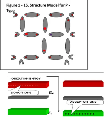
Question (9)
What is meant by the expression complete ionization? Solution
Figure 1 15. Structure Model for P -Type
In case of complete ionization, the density of holes equals to density of the acceptor ions denoted by negative charge slightly above the acceptor, band energy level.
Question (10)
How you can differnate between the both conduction material types? Solution
In the n-type material, the concentration of electrons is much larger than of holes (n>p), and the current is due to electrons and the conduction is occurred in the conduction band. In the p-type material, the concentration of holes is much larger than of electrons (p>n), and the current is due to holes, and the conduction is occurred in the valance band.
Question (11)
How you can compare between intransic , extrinsic, compensated material? Solution
In the case of Intransic material, electron concentration is equal to hole
concentration (n = p), and Fermi level is in the middle of energy gap
In the case of Extrinsic material, electron concentration is not equal to hole
concentration. In the case of n-type (n > p), where the conduction occurred by electrons in conduction band and Fermi level is shifted upward in the direction
of conduction band, and a new level named donor level, ED, exists. If (p>n),
results p-type material, conduction occurred by holes in valance band and a
new level acceptor level, EA, exists.
In the case of compensated material, NA- = ND+ we have extrinsic material have
the same properties of intrinsic
Question (12)
How you can compare between majority, and minority charge carriers in the Extrinsic material?
In the electrical neutrality law ni2 =np ,
In the n-type , electrons is majority and it can be written as nn and p the
holes is minority and it can be written as pn, so we can write the
electrical neutrality law as : ni2=nn pn ,
𝐩𝐧 = 𝐧𝐢
𝟐
𝐧𝐧 =
𝐧𝐢𝟐
𝐍𝐃
For p-type, p is majority and it written as pp, and electrons are minority and it
written as np, so we can write electrical neutrality law for p-type as:
ni2= pp np , 𝐧𝐩 = 𝐧𝐢𝟐 𝐏𝐩 = 𝐧𝐢𝟐 𝐍𝐀 Question (13)
what determine the probability that a given energy state occupies by electron? Solution
The accurate number of electrons dN having a value of energy in each range of
energy state E+ E at absolute temperature can be expressed by FERMI as:
𝒅𝑵 = 𝑪√𝑬𝒅𝑬 𝒆(𝑬−𝑬𝑭)⁄𝑲𝑻+𝟏 100% 50% 0 EC EF EV
Ef is defined as the highest electronic energy at absolute temperature. At E = Ef,
the probability of electron occupancy is 50%. It is important to note that, at 0K all the charge carriers frozen and lies in the lowest level of the energy gap. In conduction band, there is large number of states has small probability of occupation, there will be only a few electrons in the conduction band. In contrast, there many states in valance band, most of them occupied and the probability of occupation is unity, so there will be only a few unoccupied energy states in valance band.
Question (14)
When the FERMI level located in middle of the energy gap? Solution
FERMI level located in middle of the energy gap, If the number of energy states in conduction and valance band are the same. In addition, if the number of electrons in conduction and valance band are the same.
Question (15)
How you can explain the dependence of conductors and semiconductors with the temperature increasing?
Solution
In metals, Conductivity decreases by increasing temperature due to greater frequency of collisions of electrons.
Intrinsic Material Extrinsic Material Conductivity 0 100 200 300 T (oK) RE SIS TI V IT Y
In semiconductor, as shown, at low temperature, the charge carriers are frozen and the resistivity is extremely high, as the temperature raises, increasing fraction of carriers to ionize and the resistivity decreases rapidly because of increasing the ionized charges. When temperature is sufficiently high, most of dopants are completely ionized. The Conductivity begins to decrease and the resistivity is increased again just as in metals. At still higher temperature, there is further sharp decrease in resistivity due to appreciable excitation of all carriers and crossing the energy gap.
Question (16)
How the electron behaves at absolute temperature in a perfect semiconductor sample without and with subjected external electric field
Solution
When an electron introduced without subjected external electric field at absolute temperature in a perfect semiconductor sample. The electron will move freely random through the crystal as shown in figure. At room temperature, valance electrons are liberated by random motion through the crystal. Under thermal equilibrium condition, the random motion of electrons leads to zero current in any direction. The thermal vibration introduced due to collisions called scattering. The scattering phenomena increased as temperature increases for a maximum scattering velocity.
If we apply electric field to the crystal, the electrons gain a force q toward the positive pole as shown, and moves with acceleration given by:
𝒂 = − 𝒒𝜺
𝒎
And current flow. After time (), the electrons suffer of collisions decreases
velocity (𝝑) between each two consecutive collisions as ∆𝝑 = a , produces what
is called drift velocity (𝝑𝒅) .
𝝑𝒅 = ∆𝝑 = 𝝁𝜺
By increasing the subjected field, the drift velocity increases, due to the increasing of kinetic energy of the electrons. When electric field is higher increased, a critical value developed and reaches maximum scattering velocity; this velocity is not more increased by increasing electric field,
Question (17)
What is the main factors affecting the mobility of charge carriers in semiconductors?
Solution
There are three main factors affecting the mobility of charge carriers in semiconductors, they are:
(M/S)
5x10⁴
Field
Temperature: As temperature increases, the thermal kinetic energy increases the vibration of atoms and the charge carriers suffer from Collisions, the dependence of mobility in temperature given by:
𝝁𝑳 = 𝑲𝑻−𝟑 𝟐⁄
Impurities: The scattering of charge carriers results from the presence of ionized donors or acceptors or impurities. This charged centers will deflect the motion of carriers by the electrostatic forces between two bodies, so the density of such centers affect the velocity; it is also being noted that, the impurity scattering decreases as temperature increases.
𝝁𝑰 = 𝑲𝑻
𝟑 𝟐⁄
𝑵𝑰
Dislocations:
Dislocation is atomic misfit, where atoms not probably arranged, so it has a considerable role of scattering carriers. For example, in germanium, the dislocations behave as acceptors, and the mobility affects by:
𝝁𝑫 = 𝑲𝑻
Now if we combine these three parameters, we have a general expression to determine such effects in mobility of charge carriers.
𝟏 𝝁 = 𝟏 𝝁𝑳 + 𝟏 𝝁𝑰+ 𝟏 𝝁𝑫 = 𝜶𝑳 𝑻 𝟑 𝟐⁄ + 𝜶 𝑰𝑻−𝟑 𝟐⁄ + 𝜶𝑫 𝑻−𝟏 Question (18)
How is the drift and diffusion currents produced in semiconductor sample? Solution
The drift current due to Transport of charge carriers under electric field produces a drift current. The current flow in a sample having electron concentration (n) given by:
Substitute in the drift velocity, gives:
𝑰𝒏 = − 𝒒𝒏(𝝁𝒏𝜺)𝑨
L
V
The same steps can be done to determine the drift current due to the hole component in p-type material,
𝑰𝒑 = 𝒒𝒑(𝝁𝒏𝒑 𝜺)𝑨
In semiconductor, both carriers are included, so:
𝑰𝑻 = 𝒒𝑨𝜺(𝒏𝝁𝒏+ 𝒑𝝁𝒑)
THE DIFFUSION CURRENT due to diffusion of charges, the concentration of charge carrier is not uniform. Diffusion of electrons or holes results from their movement from higher concentration to lower concentration with gradient d/dx where
concentration of carriers is not distributed uniform and varieswith distance x.
Drift Electron Current I
n
Cross Sectional Area
Diffusion Of Electron Current I
n
Electron Concentration
So that, the diffusion current due to electrons given by:
𝑰𝒏 = 𝒒𝑨𝑫𝒏 𝝏𝑵
𝝏𝒙
And, the diffusion current due to holes is given by:
𝑰𝒑 = −𝒒𝑨𝑫𝒑 𝝏𝑷
𝝏𝒙
The total current of electrons and holes components given by the summing of its diffusion and drift currents as:
𝑰𝒏 = 𝒒𝑨 (𝒏𝝁𝒏𝑬 + 𝑫𝒏 𝝏𝒏 𝝏𝒙 ⁄ ) 𝑰𝒑 = 𝒒𝑨 (𝒑𝝁𝒑 𝑬 + 𝑫𝒑 𝝏𝒏 𝝏𝒙 ⁄ ) Question (19)
What is the parameters considered To calculate the flux (F) at a position (x), in semiconductor sample?
Solution
To calculate the flux (F) at a position (x), in semiconductor sample, it is average
of fluxes at positions (x – a/2) and at (x + a/2), these two fluxes given by (f1– f2),
and (f3– f4).Consider component (F1), is product of:
1. Intensity per unit area for impurities (charges) at the potential valley at (x – a).
2. The probability of a jump of any of these impurities (charges) to the next valley
at position (x)
3. The frequency of attempted jump (ⱱ)
Thus, we can write:
𝑭𝟏 = [𝒂𝑪(𝒙 − 𝒂)]𝒆𝒙𝒑 − 𝒒
𝑲𝑻(𝑾 −
𝟏
𝟐 𝒂𝝐)(ⱱ)𝑬𝒒(𝟏 − 𝟗𝟎)
Where, [𝒂𝑪(𝒙 − 𝒂)] is the density per unit area of the particles situated in
the valley at (x – a) to the valley at position (x), and (ⱱ)is frequency of attempted jump note that, the lowering of the barrier due to the electric
field (ε). Similar formulas can be written for (F2), (F3), and (F4). By combined
them to give a formula for the flux (F) at position (x),
𝑭(𝒙)= - (ⱱ𝒂𝟐 𝒆−𝒒𝑾 𝑲𝑻⁄ )𝝏𝑪 𝝏𝒙 𝒄𝒐𝒔𝒉 𝒒𝒂𝜺 𝟐𝑲𝑻+ (𝟐𝒂ⱱ𝒆 −𝒒𝑾 𝑲𝒕⁄ )C sinh -𝒒𝒂𝜺 𝟐𝑲𝑻
As extremely important, limiting from of this equation is obtained for the
case when the electric field is relatively small, i.e., ε «KT/q a. In this case,
we can expand the cosh and the sinh terms in the equation. Noting that
cosh (x) = 1 and sinh (x) = x for x → 0, this results in the limiting form of the
flux equation for a positively charged spices.
𝑭(𝒙) = − 𝑫 𝝏𝑪
𝝏𝒙 + 𝝁𝜺𝑪 ,
Chapter two
Question (19)
How a pn junction is formed? Solution
If two pieces of semiconductor materials with different conduction type are brought together in a contact, a junction is formed. Before contact there is a large electron concentration in the n-side and a large hole concentration in the p-side. After the two sides are brought into contact, electrons are diffused from the n-side to the p-n-side and holes are diffused from the p-n-side to the n-n-side. However, each electron that diffuses into the p-side leaves a positively charged donor atom behind in the n-side, likewise the holes that diffuse into the n-side leaves a negatively charged acceptor atom behind in the p-side. An electric field is built-up between the ionized donors and acceptor atoms in such a direction as to oppose further diffusion of electrons and holes and the system comes into equilibrium statement.
Question (21)
How pn junction comes in equilibrium statement? Solution
If two pieces of semiconductor materials with different conduction type are brought together in a contact, a junction is formed. Before contact there is a large electron concentration in the n-side and a large hole concentration in the p-side. After the two sides are brought into contact, electrons are diffused from the n-side to the p-n-side and holes are diffused from the p-n-side to the n-n-side. However, each electron that diffuses into the p-side leaves a positively charged donor atom behind in the n-side, likewise the holes that diffuse into the n-side leaves a negatively charged acceptor atom behind in the p-side. An electric field is built-up between the ionized donors and acceptor atoms in such a direction as to oppose further diffusion of electrons and holes and the system comes into equilibrium statement. DISTRIBUTION OF ACCEPTORS CONCENTRATION NA = 1022/cm3 DISTRIBUTION OF DONORS CONCENTRATION ND = 1022/cm3
ELECTRIC FIELD DISTRIBUTION DUE TO ACCEPTORS
ELECTRIC FIELD DISTRIBUTION DUE TO DONORS ++ ++ ++ +
-+
+
Question (22)
Compare between symmetrical and unsymmetrical pn junctions? Solution
Symmetrical junctions have equal and opposite doping on two sides, to the
left of junction, Where ND = NA ,Xm = Xn + Xp , and Xn = Xp
Question (23)
Why the depletion region acts as insulating region Solution
The depletion region acts as insulating region, since it contains no mobile carriers.
Question (24)
How you imagine the developing of the depletion region Xm for unsymmetrical
pn junction? Solution
for unsymmetrical pn junction, for example n – material (n+- p). Most of depletion
layer extends into the side has the lowest concentrations. It realized, that charge neutrality must maintained as many positive charges as negative charges must presented in space charge of the depletion region.
Question (25)
Draw a block energy band diagram for np junction, showing all the energy levels and its location in the two sides?
Solution
Note, acceptor levels in the p-type side and the donor levels in the n-type side,
most of them are ionized at room temperature (ND+ and ND+ ) . Since equilibrium
is a condition that cannot support current flow in an external wire joining the p and n regions, the energy of electrons and holes must be equal in the two regions. The Fermi level must be a single level through the material.
Question (26)
Why the depletion layer in pn diode is considered as the heart of the diode? Solution
The depletion layer in pn diode is considered as the heart of the diode, since all the electrical phenomena are occurred.
Question (27)
At the same concentration of electrons in a sample, and the same concentration of holes in a sample, we find the electron current is greater than the hole current, It seems that the conduction is due to electrons, explain such phenomena?
n- type p-type CBT CBT CBL CBL ND+ ND EF EF NA NA EVT EVT EVL EVL
Solution
𝑰𝑻 = 𝒒𝑨𝜺(𝒏𝝁𝒏+ 𝒑𝝁𝒑)
In intrinsic, 𝒏 = 𝒑 = 𝒏𝒊 , note that n >p, so in an intrinsic material the electrons
contribute more to conductivity than holes. It seems that the conduction is due to electrons, so the conduction in intrinsic material considered as in n-type material. So, if we consider the cross-sectional area A for the sample are equal
and 𝜺 in relation with the mobility , Let us consider the value of (𝒒𝑨𝜺 ) in the
current equation which simplified to 𝑰𝑻 = (𝒏𝝁𝒏+ 𝒑 𝝁𝒑) and the material under
consideration has n = p , then 𝑰𝑻 𝜶 (𝝁𝒏+ 𝝁𝒑) , and since 𝝁𝒏 > 𝝁𝒑 , then we
neglect the current due to holes and the total current is depend only with 𝝁𝒏 and
the total current considered as electron current 𝑰𝑻 𝜶 (𝝁𝒏)
Question (28)
In symmetrical pn junction , we find the electron current is greater than hole current, and we consider that the current due to electrons neglecting the hole current, explain such phenomena
Soluton As in Question (27)
10
-510
-410
-310
-210
-1For N-Type Materials
For P-Type materials
Question (29)
Why we consider that the current in intrinsic sample as as in n-type material? Solution
𝑰𝑻 = 𝒒𝑨𝜺(𝒏𝝁𝒏+ 𝒑 𝝁𝒑)
In intrinsic, 𝒏 = 𝒑 = 𝒏𝒊 , note that n >p, so in an intrinsic material the electrons
contribute more to conductivity than holes. It seems that the conduction is due to electrons, so the conduction in intrinsic material considered as in n-type material. So, if we consider the cross-sectional area A for the sample are equal
and 𝜺 in relation with the mobility , Let us consider the value of (𝒒𝑨𝜺 ) in the
current equation which simplified to 𝑰𝑻 = (𝒏𝝁𝒏+ 𝒑 𝝁𝒑) and the material under
consideration has n = p , then 𝑰𝑻 𝜶 (𝝁𝒏+ 𝝁𝒑) , and since 𝝁𝒏 > 𝝁𝒑 , then we
neglect the current due to holes and the total current is depend only with 𝝁𝒏 and
the total current considered as electron current 𝑰𝑻 𝜶 (𝝁𝒏)
Question (30)
In reverse bias condition, the current will disappear, explain? Solution
In reverse bias condition, the current will disappear, since the holes in the p - side, and electrons in the n - side are move away from the junction. Because in the reverse bias the barrier voltage is increased and charge carriers is decreased and the depletion layer thickness increased. And constitute small current known as
reverse saturation current IR or Io or Is .
Question (31)
How you can explain the forward and reverse bias condition? Solution
In forward bias, height of potential barrier decreased than the nominal value of VT increases flow of majority carrier’s (pP), and (nn), and the charge carriers
increased and current flow depend with VF
In reverse bias, height of potential barrier increased than the nominal value of VT,
reduces flow of majority carrier’s (pP), and (nn), also reduce flow of minority
carriers (pn), and (np). and current will be equal reverse saturation current (IR) , it
is a constant not depend with VR until certain limit. Until reverse voltage becomes
very large, then at critical voltage a large current surge through the diode and junction breakdown is occurred. It can damage the diode
Question (32)
Draw the IV characteristics for the diode at both the forward and reverse bias condition? Solution Question (33) Question (32)
I
F(ma) I
F(ma)
5 5
4 4
3 3
2 2
1 1
V
RV
F0.2 0.4 0.6
0.2 0.4 0.6
V
ZI
OQuestion (33)
What are the currents exists in the diode , can you write the equation for each component?
Solution
there are two components of current density flowing across the junction.
Current density component J1n is the component of the current density that
flows down the potential barrier with the electron flowing from p-region to n-region and it is the drift current density due to the free electrons under the
influence of the field because the potential barrier and J1n may be written as:
𝑱𝟏𝒏 = 𝒒𝒏𝝁𝒏𝜺 (𝟐. 𝟐)
Current density component J2n flow of electrons from n-region where free
electrons are majority carriers to p-region where they become minority current flows due to diffusion, thus,
𝑱𝟐𝒏 = 𝒒𝑫𝒏𝒅𝒏
𝒅𝒙(𝟐. 𝟑)
When applied, voltage is zero, sum of the two components is equal to zero, hence:
𝑱𝟏𝒏+ 𝑱𝟐𝒏 = 𝒒𝒏𝝁𝒏𝜺 + 𝒒𝑫𝒏𝒅𝒏
𝒅𝒙 = 𝟎 (𝟐. 𝟒)
𝑱𝟏𝒑 + 𝑱𝟐𝒑 = 𝒒𝒑𝝁𝒏𝒑𝜺 + 𝒒𝑫𝒑𝒅𝒑
𝒅𝒙 = 𝟎
So, there are four current components Two diffusion currents
(𝒒𝑫𝒏𝒅𝒏
𝒅𝒙 𝒂𝒏𝒅 𝒒𝑫𝒑
𝒅𝒑
𝒅𝒙) and two drift currents (𝒒𝒏𝝁𝒏𝜺 𝒂𝒏𝒅 𝒒𝒑𝝁𝒏𝒑𝜺). The total
current flowing will be nearly equal to sum of electron and hole diffusion currents at junction.
Question (34)
Draw the IV characteristics for the diode at both the forward and reverse bias condition as dependent on temperature?
T3> T2> T1
We deduce that, I/t = 0.08% /oC for Si, 0.11%/oC for Ge, also we have found
that the reverse saturation current increases by 7%/oC for Ge, Si. We conclude
that the reverse saturation current double it self-every 10oC rise in temperature.
The much larger value of the reverse saturation current for Ge than for Si, and since the temperature dependence is the same for both materials, then the elevated temperature in Ge devices will develop an excessive large reverse saturation current, where for Si, reverse saturation current will be quite modest. For more clarification, an increase in temperature from room temperature to 90
oC increases the reverse saturation current for Ge to hundreds of microamperes,
in Si it rises to tenth of microamperes
Reverse Bias Forward BiasV
J -V J
T
1T
2T
3 -IIdeal Curve Real curve
Question (35)
How you can explain that at same applied voltage, the current in Ge diode is more than the current in Si diode?
Problem (1):
Solution
As shown in figure, that at the same applied voltage, the current in Ge diode is greater than in Si diode, that is because the mobility of charge carriers in Ge diode
is greater than in Si diode. Normally, n > p for any material. For example, in
silicon n = 1800, p = 400 cm2/V. sec, and in germanium we find that n = 3800,
p = 1800 cm2/V. sec. The currents depended on the value of mobility. at same,
applied voltage, the current in Ge diode is more than the current in Si diode
Question (36)
How we can express such expressions, Applied voltage (Vo) , built – in or , barrier
voltage (VT) , forward voltage (VF) , reverse voltage (VR) , cut-in or offset or break
point or threshold voltage (V) , Zener or breakdown voltage (VZ)?
Solution I(ma) 10 8 6 4 2 1 0 0.2 0.4 0.6 0.8 1.00 V(Volt)
VG VSi For Ge Devices For Si Devices
10 mA
Applied voltage (Vo), is the battery voltage applied to in semiconductor diode
circuit, it can be positive or negative to be forward or reverse.
built – in or, barrier voltage (VT), is the voltage that be built – up during the pn
contact construction to hinder more diffusion of both charge carriers and bring the system in neutral electric mode.
forward voltage (VF), is the applied voltage to pn device, it decreases the
barrier voltage and increase charge carrier concentration and bring the diode in forward bias mode.
reverse voltage (VR), is the applied voltage to pn device, it increases the barrier
voltage and decrease charge carrier concentration and bring the diode in reverse bias mode.
cut-in or offset or break point or threshold voltage (V), is greater than the
barrier voltage, it is in forward bias mode but below which forward below which forward current is very small, less than 1% of its maximum.
Zener or breakdown voltage (VZ) , is in reverse bias mode , when reverse
voltage increases for a certain value , rush of reverse saturation current can damage the diode.
Question (37)
How we can express such expressions, forward current (IF), reverse current (IR),
reverse saturation current (IS) cut-in current (I) , Zener or breakdown current (IZ)?
Solution
Forward current (IF), in forward bias mode current flow between the diode
terminal, it is due to majority charge carriers, this current depend on the forward voltage, it has nonlinear behavior at certain forward voltage, less more forward voltage then it has linear characteristic
Reverse current (IR), in reverse bias mode, the current between the diode
terminal disappeared, it is due to minority charge carriers, this current is constant not depend on the reverse voltage.
Reverse saturation current (IS), in reverse bias mode, the current between
the diode terminal disappeared, it is due to minority charge carriers, this current is constant not depend on the reverse voltage.
Cut-in current (I), in forward bias mode current flow between the diode
levels which ionized first before the ionization of large concentration of carriers, this current exist in the range of built -in voltage and cut-in voltage, its value is not more than 1% of the maximum forward current.
Zener or breakdown current (IZ), in reverse bias mode, the reverse saturation
current is existing, it is due to minority charge carriers, this current is constant
not depend on the reverse voltage until certain reverse voltage (VZ). then
higher current is flow; this current can damage the diode.
Question (38)
Which types of resistance, we have in the pn diodes? Solution
we have two possible resistances to consider:
DC resistance; Dc resistance of the modelling diode combination is
𝑹𝒅𝒄 = RT - (𝑹𝒏+ 𝑹𝒑);
The Dc resistance of ideal part of diode, (rdc) can be calculated from:
𝒓𝒅𝒄 = 𝑽𝑱
𝑰𝑱 =
𝑽𝑱
𝑰𝑺 𝒆𝒙𝒑 [𝒒𝑽𝑲𝑻𝑱 − 𝟏]
Dynamic or small signal resistance (ac resistance) (ra) an important
parameter and it is equal,
𝒓𝒂 = 𝝏𝑽
𝝏𝑰
Rn VJ RP
Dynamic resistance ra is not constant depends upon the voltage and we find
that the dynamic conductance for PN ideal diode is given by:
𝒈 = 𝟏 𝑹= 𝝏𝑰 𝝏𝑽 = 𝑰𝒐𝒆𝑽⁄𝜼𝑽𝑻 𝜼𝑽𝑻 = 𝑰 + 𝑰𝒐 𝜼𝑽𝑻
For reverse bias, where V/VT << 1, conductance g = 1/R will be very small and
dynamic resistance r is very large. For forward bias, where V/VT >> 1 , I >> Io
and dynamic resistance r is given by:
𝒓𝒂 = 𝜼𝑽𝑻 𝑰
Ac resistance rac of ideal diode determined from slope of C.C at the operating
points or determined analytically as follows. It is convenient to calculate ac
conductance (gac),
𝑰𝑱 = 𝑰𝑺𝒆𝒙𝒑 [𝒒𝑽𝑱
𝑲𝑻 − 𝟏]
Ac resistance of real diode is then,
𝑹𝒂𝒄 = 𝒓𝒂𝒄+ 𝑹𝒏 + 𝑹𝒑
𝑹𝒂𝒄 = 𝑲𝑻
𝒒 (
𝟏
𝑰𝒔 + 𝑰𝑱) + 𝑹𝒏 + 𝑹𝒑
At room temperature, value of Rac,
𝒓𝒂𝒄 = 𝟐𝟓
𝑰𝒔 + 𝑰𝑱𝒐𝒉𝒎
Note that in some cases the ohmic series resistance will be important and in other is not. At very high current the forward ideal diode resistance becomes negligible compared with the series resistance. Since the series resistance in the real diode C.C becomes ohmic at high currents.
Question (39)
What are the parameters on which the junction current depend upon? Solution
Parameters on which the junction current depend upon are: physical properties of the junction, properties of the crystal, density of impurities, impurity distribution, and many other factors.
Question (40)
Draw a complete equivalent circuit for P-N diode? Solution
RJ
Total of the resistance combination is = RDC in series with combination of junction
resistance and capacitance which are in parallel connection RT = RDC + (RJ // CJ ) = (𝑹𝒏+ 𝑹𝒑) + (RJ // CJ )
CJ is the junction capacitance due to depletion layer which exhibits the behavior
of a capacitance having the same geometry and dielectric constant.
𝒒𝑵𝑨𝒙𝒑 = 𝒒𝑵𝑫𝒙𝒏
Problem (1)
Write the electronic configuration of silicon has 14 electrons in its atom,
determine in which sub shell and in which orbit and how many electrons in the highest sub shell energy.
Solution:
The electronic configuration of silicon as follows, 1S2 2S2 2p6 3S2 3p2
The highest sub shell energy lies in (M) orbit, in the sub shell (p) which is not fully occupied, it has only 2 electrons
problem (2)
Calculate the conductivity and the resistivity of n-type silicon wafer, which
contains 1016 electrons per cubic centimeter with an electron mobility of 1400
cm2/Vs.
Solution:
The conductivity is obtaining by adding the product of the electronic charge, q, the carrier mobility, and the density of carriers of each carrier type, or:
𝝈 = 𝒒(𝒏𝝁𝒏+ 𝒑𝝁𝒑)
As n-type material contains almost no holes, the conductivity equals:
𝝈 = 𝒒𝒏𝝁𝒏 = 𝟏. 𝟔𝒙𝟏𝟎−𝟏𝟗 𝒙𝟏𝟒𝟎𝟎𝒙𝟏𝟎𝟏𝟔 = 𝟐. 𝟐𝟒 𝟏𝜴𝒄𝒎
The resistivity equals the inverse of the conductivity
𝝆 = 𝟏 𝝈 = 𝟏 𝒒(𝒏𝝁𝒏+ 𝒑𝝁𝒑) In addition, equals ρ = 1/ σ = 1/2.24 = 0.446 Ω cm Problem (3)
A silicon wafer contains 1016 cm-3 electrons. Calculate the hole density and the
position of the intrinsic energy and the Fermi energy at 300 K. Draw the corresponding band diagram to scale, indicating the conduction and valence band
edge, the intrinsic energy level and the Fermi energy level. Use ni = 1010 cm-3.
Solution:
The hole density is obtained using the mass action law:
𝒑 = 𝒏𝒊
𝟐
𝒏 =
𝟏𝟎𝟐𝟎
𝟏𝟎𝟏𝟔 = 𝟏𝟎𝟒𝒄𝒎−𝟑
𝑬𝒊− 𝑬𝒄+ 𝑬𝒗 𝟐 = − 𝟑 𝟒 𝑲𝑻𝒍𝒏 𝒎𝒉∗ 𝒎𝒆∗ = 𝟑 𝟒 𝒙𝟎. 𝟎𝟐𝟓𝟖𝒍𝒏 𝟎. 𝟖𝟏 𝟏. 𝟎𝟖= 𝟓. 𝟓𝟖𝒎𝒆𝑽
The position of the Fermi energy relative to the intrinsic energy equals:
𝑬𝑭− 𝑬𝒊 = 𝑲𝑻𝒍𝒏 (𝑵𝒅
𝒏𝒊) = 𝟎. 𝟎𝟐𝟓𝟖𝒍𝒏
𝟏𝟎𝟏𝟔
𝟏𝟎𝟏𝟎 = 𝟑𝟓𝟕𝒎𝒆𝑽
Problem (4)
A piece of silicon has a resistivity which is specified by the manufacturer to be
between 2 and 5 Ohm cm. If the mobility of electrons is 1400 cm2/V-sec and that
of holes is 450 cm2/V-sec, what is the minimum possible carrier density and what
is the corresponding carrier type? Repeat for the maximum possible carrier density.
Solution
The minimum carrier density obtained for the highest resistivity and the material with the highest carrier mobility, i.e. the n-type silicon. The minimum carrier density therefore equals:
𝒏 = 𝟏
𝒒𝝁𝒏𝝆𝒎𝒂𝒙 =
𝟏
𝟏. 𝟔𝒙𝟏𝟎−𝟏𝟗𝒙𝟏𝟒𝟎𝟎𝒙𝟓= 𝟖. 𝟗𝟐𝒙𝟏𝟎
𝟏𝟒𝒄𝒎−𝟑
The maximum carrier density obtained for the lowest resistivity and the material with the lowest carrier mobility, i.e. the p-type silicon. The maximum carrier density therefore equals:
𝒑 = 𝟏 𝒒𝝁𝒑𝝆𝒎𝒂𝒙 = 𝟏 𝟏. 𝟔𝒙𝟏𝟎−𝟏𝟗 𝒙𝟒𝟓𝟎𝒙𝟐= 𝟔. 𝟗𝟒𝒙𝟏𝟎 𝟏𝟓𝒄𝒎−𝟑 Problem (5)
Calculate the intrinsic carrier density in silicon at 300, 400, 500 and 600 oK. if the
effective density of electrons in conduction band is 𝟐. 𝟖𝟏𝒙𝟏𝟎𝟏𝟗 and the
effective density of holes in valance band is 𝟏. 𝟖𝟑𝒙𝟏𝟎𝟏𝟗 .
Solution
𝒏𝒊(𝟑𝟎𝟎𝑲) = √𝑵𝒄𝑵𝒗𝒆𝒙𝒑 (−𝑬𝒈
𝟐𝑲𝑻)
= √𝟐. 𝟖𝟏𝒙𝟏𝟎𝟏𝟗𝒙𝟏. 𝟖𝟑𝒙𝟏𝟎𝟏𝟗 𝒆𝒙𝒑 ( −𝟏. 𝟏𝟐
𝟐𝒙𝟎. 𝟎𝟐𝟓𝟖)
= 𝟖. 𝟕𝟐𝒙𝟏𝟎𝟗𝒎−𝟑
To get the value of T differ than room temperature (300 oK) , and since Boltzmann
constant is not given , so we can get the required value from the ratio between
the value of KT at 300 oK (0.026 eV) and its value at 400 oK ,
At 300 oK = 0.026 eV , then KT at 400 oK is 400 x 0.026 / 300 = 0.0346 eV So, 𝒏𝒊(𝟒𝟎𝟎𝑲) = √𝑵𝒄𝑵𝒗𝒆𝒙𝒑 ( −𝑬𝒈 𝟐𝑲𝑻) = √𝟐. 𝟖𝟏𝒙𝟏𝟎𝟏𝟗𝒙𝟏. 𝟖𝟑𝒙𝟏𝟎𝟏𝟗 𝒆𝒙𝒑 ( −𝟏. 𝟏𝟐 𝟐𝒙𝟎. 𝟎𝟑𝟒𝟔) = 𝟒. 𝟓𝟐 𝐱 𝟏𝟎𝟏𝟐 𝒆𝒍𝒆𝒄𝒕𝒓𝒐𝒏𝒔 𝒊𝒏 𝒎−𝟑 At 300 oK = 0.026 eV , then KT at 500 oK is 500 x 0.026 / 300 = 0.0433 eV 𝒏𝒊(𝟓𝟎𝟎𝑲) = √𝑵𝒄𝑵𝒗 𝒆𝒙𝒑 (−𝑬𝒈 𝟐𝑲𝑻) = √𝟐. 𝟖𝟏𝒙𝟏𝟎 𝟏𝟗 𝒙𝟏. 𝟖𝟑 𝒙𝟏𝟎𝟏𝟗 𝒆𝒙𝒑 ( −𝟏. 𝟏𝟐 𝟐𝒙 𝟎. 𝟎𝟒𝟑𝟑) = 𝟐. 𝟏𝟔 𝐱 𝟏𝟎 𝟏𝟒 𝒆𝒍𝒆𝒄𝒕𝒓𝒐𝒏𝒔 𝒊𝒏 𝒎−𝟑 At 300 oK = 0.026 eV , then KT at 600 oK is 400 x 0.026 / 300 = 0.052 eV 𝒏𝒊(𝟔𝟎𝟎𝑲) = √𝑵𝒄𝑵𝒗 𝒆𝒙𝒑 ( −𝑬𝒈 𝟐𝑲𝑻) = √𝟐. 𝟖𝟏𝒙𝟏𝟎𝟏𝟗 𝒙𝟏. 𝟖𝟑𝒙𝟏𝟎𝟏𝟗 𝒆𝒙𝒑 ( −𝟏. 𝟏𝟐 𝟐𝒙 𝟎. 𝟎𝟓𝟐) = 𝟑. 𝟎𝟕 𝐱 𝟏𝟎 𝟏𝟓 𝒆𝒍𝒆𝒄𝒕𝒓𝒐𝒏𝒔 𝒊𝒏 𝒎−𝟑 Temperature oK 300 400 500 600 Intrinsic concentration 8.72 x 10⁹ 4.52 x 10¹² 𝟐. 𝟏𝟔 𝐱 𝟏𝟎𝟏𝟒 𝟑. 𝟎𝟕 𝐱 𝟏𝟎𝟏𝟓 Change % above RT --- 5.183 % 247.7% 3520%