Near Data Processing for Efficient and Trusted Systems
by Shaizeen Aga
A dissertation submitted in partial fulfillment of the requirements for the degree of
Doctor of Philosophy
(Computer Science and Engineering) in The University of Michigan
2018
Doctoral Committee:
Associate Professor Satish Narayanasamy, Chair Professor Todd Austin
Assistant Professor Reetuparna Das Professor Mingyan Liu
Shaizeen Aga [email protected] ORCID iD: 0000-0001-9552-0508
c
To my parents for their courage to defy norms:
My mother, Sherbanu Aga
ACKNOWLEDGEMENTS
The path from dreams to success does exist.
May you have the vision to find it,
the courage to get on to it,
and the perseverance to follow it.
Wishing you a great journey.
-Kalpana Chawla, Indian-American Astronaut
Her message aboard the space shuttle Columbia to students of her college in India.
First and foremost, I would like to express my gratitude to my parents. They have been a constant source of support and encouragement throughout my life. It is thanks to their courage to defy social norms which discouraged letting a girl child pursue education that I am here today. Many thanks also to my school and undergraduate professors who helped me believe in myself.
This dissertation is a product of countless interactions with my advisor Professor Satish Narayanasamy. I am grateful to him for encouraging me to pursue a doctorate when I wasn’t very confident in my ability to conduct research. He has helped and guided me over the entire course of my graduate studies. He has contributed immensely in my transforma-tion into a computer scientist who can think critically, express ideas crisply and for that I
will forever be grateful to him.
I am also grateful to my amazing committee members Professor Todd Austin, Professor Reetuparna Das, Professor Mingyan Liu and Professor Scott Mahlke for their insightful comments on my research and for taking time out to evaluate my dissertation. Specifically, Professor Reetuparna Das advised me on my Compute Caches project and her enthusiasm for this work helped me overcome various hurdles.
I have had the pleasure to collaborate with many worthy researchers and fellow graduate students over the course of my graduate studies. I am grateful to Sriram Krishnamoorthy from Pacific Northwest National Labs for his patience and help during my CilkSpec project. I am also grateful to Abhay Singh for countless discussions on memory models and his ability to discuss any technical topic under the sun with ease. Thanks to Supreet Jeloka who helped me understand the intricacies of SRAMs and Arun Subramaniyan for his help with Compute Caches project. Many thanks to Byoungchan Oh for helpful discussions on memories and Salessawi Ferede Yitbarek for always being encouraging and being ever so ready to discuss new research ideas. Finally, thanks to my lab-mates Chun-Hung Hsiao and Subarno Banerjee for many useful discussions.
Over the course of my time at University of Michigan, I have been blessed to have an amazing group of friends who have helped me immensely. Thanks to Daya for being super-helpful and for always being available to answer my questions. Thanks to Ankit for being a constant source of support and his poor jokes. Thanks to Divya and Megha for amazing food.
Last but not the least I would like to sincerely thank my extended family who make life worth living. Neel, for showing me the bright side of things and endeavoring to make me
happy. My amazing roommate Komal for countless discussions on surviving graduate life. My super supportive set of friends Trupti and Akshay for whole heartedly believing in my ability to achieve anything I put my mind to.
TABLE OF CONTENTS
DEDICATION . . . ii ACKNOWLEDGEMENTS . . . iii LIST OF FIGURES . . . ix LIST OF TABLES . . . xi ABSTRACT. . . xii CHAPTER I. Introduction . . . 11.1 Compute Caches: Efficient Very Large Vector Processing . . . 3
1.2 InvisiMem: Smart Memory Defenses for Memory Bus Side Channel 4 1.3 Sanctuary: Secure and Efficient Memory Management . . . 6
1.4 Organization . . . 8
II. Background . . . 9
2.1 NDP proposals without 3D Stacked Memory . . . 9
2.2 3D Stacked Memory . . . 12
2.2.1 NDP proposals with 3D Stacked Memory . . . 12
2.3 Breaking New Ground in NDP . . . 13
III. Compute Caches: Caches that Compute . . . 14
3.1 Introduction . . . 14
3.2 Background . . . 18
3.2.1 Cache Hierarchy and Geometry . . . 18
3.2.2 Bit-line Computing . . . 19
3.3 A Case for Compute Caches . . . 20
3.4.1 Instruction Set Architecture (ISA) . . . 23
3.4.2 Cache Sub-arrays with In-Place Compute . . . 24
3.4.3 Operand Locality . . . 26
3.4.4 Managing Parallelism . . . 29
3.4.5 Fetching In-Place Operands . . . 30
3.4.6 Cache Coherence . . . 32
3.4.7 Consistency Model Implications . . . 33
3.4.8 Memory Disambiguation and Store Coalescing . . . 33
3.4.9 Error Detection and Correction . . . 35
3.4.10 Near-Place Compute Caches . . . 35
3.5 Applications . . . 36
3.6 Evaluation . . . 38
3.6.1 Simulation Methodology . . . 38
3.6.2 Application Customization and Setup . . . 38
3.6.3 Compute Sub-Array: Delay and Area Impact . . . 40
3.6.4 Microbenchmark Study . . . 41
3.6.5 Application Benchmarks . . . 44
3.7 Related Work . . . 46
3.8 Discussion . . . 49
3.9 Conclusion . . . 51
IV. InvisiMem: A Low-overhead Secure Processor . . . 52
4.1 Introduction . . . 52
4.2 Motivation and Background . . . 57
4.2.1 Enclaves for Isolation . . . 58
4.2.2 Threat Model . . . 59
4.2.3 Memory Bus Side Channel and Cold Boot Defenses . . 60
4.2.4 Smart Memory . . . 62
4.3 InvisiMem Design . . . 63
4.3.1 Advantages of Smart Memory . . . 63
4.3.2 Protecting Memory Address and Type . . . 64
4.3.3 Guaranteeing Data Integrity and Freshness . . . 65
4.3.4 Mitigating Memory Bus Timing Channel . . . 66
4.3.5 Performance: OTP Pre-computation . . . 68
4.3.6 Space: Meta-Data in Smart Memory . . . 69
4.3.7 Remote Attestation and Key Exchange . . . 70
4.3.8 Key and Timestamp Management . . . 72
4.3.9 Near InvisiMem . . . 73
4.4 Implementation . . . 74
4.4.1 Hardware Support for Cryptographic Primitives . . . 74
4.4.2 InvisiMem far Security Protocol . . . 76
4.4.3 InvisiMem near Security Protocol . . . 77
4.4.4 Storing Meta-Data in Smart Memory . . . 77
4.5.1 Methodology . . . 78
4.5.2 Unsecure Smart Memory Performance and Energy . . . 81
4.5.3 Far InvisiMem . . . 82
4.5.4 Static Packet Rate for Timing Channel . . . 83
4.5.5 Near InvisiMem . . . 85
4.5.6 Memory Space Overhead . . . 85
4.5.7 Fragmented Vs Non-Fragmented . . . 86
4.6 Related Work . . . 87
4.6.1 3D Stacking for Security . . . 87
4.6.2 Secure Hardware . . . 87
4.7 Conclusion . . . 89
V. Sanctuary: Efficient Page Fault Channel Defense . . . 90
5.1 Introduction . . . 91
5.2 Motivation and Background . . . 96
5.2.1 Intel SGX . . . 96
5.2.2 Threat Model . . . 97
5.2.3 Path Oblivious RAM . . . 98
5.3 Sanctuary Design . . . 100
5.3.1 Secure Runtime . . . 100
5.3.2 Oblivious Page Management . . . 101
5.3.3 EPC-lite to reduce OPAM reliance . . . 110
5.4 Sanctuary Implementation . . . 112
5.4.1 Sanctuary Metadata . . . 112
5.4.2 OPAM Implementation . . . 115
5.5 Applications and Security Context . . . 117
5.6 Evaluation . . . 120
5.6.1 Methodology . . . 120
5.6.2 Memory Footprint of Applications . . . 122
5.6.3 Evaluation of Smart Tree Growth . . . 123
5.6.4 Benefits of Thin Nodes . . . 124
5.6.5 Sanctuary Performance . . . 125
5.7 Related Work . . . 127
5.7.1 Secure Hardware Proposals . . . 127
5.7.2 Prior Page Fault Channel Mitigations . . . 128
5.7.3 Optimizing SGX Performance . . . 129
5.8 Conclusion . . . 129
VI. Conclusion . . . 131
LIST OF FIGURES
Figure
3.1 Compute Cache overview. (a) Cache hierarchy. (b) Cache geometry (c) In-place compute in a sub-array. . . 18 3.2 SRAM circuit for in-place operations. Two rows (WLi and WLj) are
activated. AnANDoperation is performed by sensing bit-line (BL). All the bit-lines are initially pre-charged to ‘1’. If both the activated bits in a column have a ‘1’ (column ‘n’), then the BL stays high and it is sensed as a ‘1’. If any one of the bits were ‘0’ it will lower the BL voltage below
Vref and will be sensed as a ‘0’. ANORoperation can be performed by sensing bit-line bar (BLB). . . 19 3.3 Proportion of energy (top) for bulk comparison operation and area
(bot-tom). Red dot depicts logic capability. . . 20 3.4 In-place copy operation (from row i to j). . . 24 3.5 Cache organization example, address decoding ([i][j] = set i, way j),
al-ternate address decoding for parallel tag-data access caches . . . 26 3.6 Compute Caches in action . . . 31 3.7 Benefit of CC for 4KB operand. a) Throughput b) Dynamic energy . . . . 41 3.8 Total energy benefit of CC for 4KB operand. . . 41 3.9 a) Total energy of in-place vs near place for 4KB operand b) Savings in
dynamic energy for 4KB operand for different cache levels . . . 43 3.10 a) Total energy benefit b) Performance improvement of CC for applications 44 3.11 Performance overhead of CC for checkpointing . . . 45 3.12 Total energy with and without checkpointing . . . 46 4.1 Smart memory based secure designs. a) InvisiMem far b) InvisiMem near 55 4.2 Symmetric encryption of addresses is not enough. (a) Distinguishing
reads from writes (b) Correlation attack . . . 64 4.3 Time taken to respond by memory can leak sensitive inputs. . . 67 4.4 Existing client-host remote attestation and key exchange (left). Smart
memory authentication and key exchange under InvisiMem (right). . . 70 4.5 InvisiMem far Security Protocol for Read.td: timestamp stored with data. 75 4.6 InvisiMem far Security Protocol for Write. . . 75 4.7 (a) Fragmented Design (b) Non-fragmented Design . . . 78
4.8 Performance overhead of far-memory processor unsecure and secure de-signs w.r.t DRAM hp. . . 81 4.9 Energy overhead w.r.t DRAM hp. . . 81 4.10 ED2 overhead w.r.t InvisiMem far without timing channel defense for
various static memory access rates. . . 83 4.11 Overheads w.r.t InvisiMem far without timing channel defense for
vari-ous static memory access rates. . . 83 4.12 Comparison to dynamic scheme. . . 84 4.13 Performance overhead of near-memory designs w.r.t DRAM hp. . . 85 5.1 Memory organization under SGX (a) and under Sanctuary (b). CFI:
Con-fidentiality, Freshness, Integrity . . . 91 5.2 Accessingblock ainvolves read and write of path to leaf to which the
block is mapped. (a) Depicts stash after end of path read. (b) Depicts stash after end of path write. Block with dummy data is represented asφ. 98 5.3 Sanctuary page table entries (PTE). A virtual address maps to EPC or
non-EPC memory. For the former, PTE is as before (a) consisting of physical page number and PTE metadata. For the latter, we store leaf and tree level (b). This allows about 8TB ofnon-EPCmemory per enclave. . . 102 5.4 Smart growth. Adding nodes to a full tree (50% utilization). Naive
growth adds nodes gradually from left to right which will cause the page addition to fail as path to leaf 7 is full. Smart growth prioritizes adding nodes to path which is accessed. As a consequence, the addition succeeds. 103 5.5 Finding page 10 in new tree which was mapped to leaf 3 in old tree. We
employ deterministic remapping; even addresses get remapped to right paths and odd addresses to left paths. We also remember tree level with the mapping. To find the page, we find leaf in tree with #old levels and traverse the tree in relevant direction based on address. . . 105 5.6 Fast background spill processing. We store past failed spills in a sorted
order (by leaf id). Figure shows access of path to leaf 3 which has one empty node (checked) to which we can potentially spill a past failed spill. We also show the leaf ranges that can be spilled to each node. Simple range checks against these leaf ranges of available failed spills can help us process past failed spills quickly. . . 109 5.7 Thin nodes optimization: page movements reduce considerably with very
small increase in tree height. . . 109 5.8 Memory footprint (accessed) of applications. . . 122 5.9 Comparison of maximum spill failures (average) for naive tree growth
and smart growth. Smart tree growth considerably reduces spill failures by prioritizing accessed paths while adding space. . . 123 5.10 (a) Realized benefit of thin nodes optimization : page moves reduce
con-siderably while OPAM events do not increase. (b) Performance overhead for existingEPCsize (96MB) with thin nodes optimization. . . 123 5.11 Performance overhead with a four channel memory system for increasing
enclave-lite memory size (total isolated memory (usable) is depicted). . . 124 5.12 EPCmisses per kilo instructions. . . 124
LIST OF TABLES
Table
3.1 Cache energy per read access . . . 21
3.2 Compute Cache ISA. . . 23
3.3 Cache geometry and operand locality constraint. . . 28
3.4 Simulator parameters . . . 38
3.5 Cache energy (pJ) per cache-block (64-byte) . . . 41
4.1 Comparison of InvisiMem to ORAM-based defenses. Smart memory en-ables more efficient and simpler solutions. . . 58
4.2 Processor and memory model. . . 79
4.3 LLC MPKI and IPC for DRAM hp. . . 79
4.4 Request and response packet sizes (in bytes). . . 80
4.5 Memory space overheads. . . 86 5.1 Instructions (in billions) and CPI for unsecure baseline (native execution). 120
ABSTRACT
Near Data Processing for Efficient and Trusted Systems by
Shaizeen Aga
Chair: Satish Narayanasamy
We live in a world which constantly produces data at a rate which only increases with time. Conventional processor architectures fail to process this abundant data in an efficient manner as they expend significant energy in instruction processing and moving data over deep memory hierarchies. Furthermore, to process large amounts of data in a cost effective manner, there is increased demand for remote computation. While cloud service providers have come up with innovative solutions to cater to this increased demand, the security concerns users feel for their data remains a strong impediment to their wide scale adoption. An exciting technique in our repertoire to deal with these challenges is near-data pro-cessing. Near-data processing (NDP) is a data-centric paradigm which moves computation to where data resides. This dissertation exploits NDP to both process the data deluge we face efficiently and design low-overhead secure hardware designs.
augmen-tations to underlying SRAM design enable caches to perform commonly used operations. In-place computation in caches not only avoids excessive data movement over memory hierarchy, but also significantly reduces instruction processing energy as independent sub-units inside caches perform computation in parallel. Compute Caches significantly improve the performance and reduce energy expended for a suite of data intensive applications.
Second, this dissertation identifies security advantages of NDP. While memory bus side channel has received much attention, a low-overhead hardware design which defends against it remains elusive. We observe that smart memory, memory with compute capa-bility, can dramatically simplify this problem. To exploit this observation, we propose InvisiMem which uses the logic layer in the smart memory to implement cryptographic primitives, which aid in addressing memory bus side channel efficiently. Our solutions obviate the need for expensive constructs like Oblivious RAM (ORAM) and Merkle trees, and have one to two orders of magnitude lower overheads for performance, space, energy, and memory bandwidth, compared to prior solutions.
This dissertation also addresses a related vulnerability of page fault side channel in which the Operating System (OS) induces page faults to learn application’s address trace and deduces application secrets from it. To tackle it, we propose Sanctuary which obfus-cates page fault channel while allowing the OS to manage memory as a resource. To do so, we design a novel construct, Oblivious Page Management (OPAM) which is derived from ORAM but is customized for page management context. We employ near-memory page moves to reduce OPAM overhead and also propose a novel memory partition to reduce OPAM transactions required. For a suite of cloud applications which process sensitive data we show that page fault channel can be tackled at reasonable overheads.
CHAPTER I
Introduction
We are constantly being bombarded with new data everyday from varied sources. Nearly 90% of data that exists today has been produced in just the last two years, and we continue to generate nearly 2.5 quintillion bytes per day [3]. Analyzing this data holds the key to answering many unsolved problems, from accurate weather prediction to personalized medicine.
This data deluge, however, has exposed us to several challenges that need addressing. First, it has brought to light severe inefficiencies in conventional architectures which were not designed with this unprecedented data deluge in mind. Second, it has brought forth new pressing needs like increased demand for secure remote computations that need efficient solutions. The focus of this dissertation is to identify these inefficiencies, new pressing needs and address them efficiently with innovative architectural solutions.
An important shortcoming of conventional architectures that we focus on in this work is their compute centric nature. Today’s conventional architectures spend large amounts of energy and time in instruction processing and data movement over deep memory hi-erarchies and very little on actual computation. Vector units available today only reduce
instruction processing overhead to some extent. This makes conventional architectures ill-equipped to run current data centric applications which process large amounts of data. Given the wealth of interesting insights this data holds, it is paramount to design architec-tures which address these inefficiencies and which can process humongous amounts of data in an efficient manner both from performance and energy perspective.
Furthermore, there is an increased demand for remote computation to process the data explosion we are facing in a cost effective manner. Cloud computing solutions are being increasingly looked up to in order to meet this demand. While cloud service providers are innovating at a lightning pace in the breadth of services they provide, from large graph pro-cessing to genetic data propro-cessing, the security concerns users feels for their data remains a strong impediment to adoption of cloud computing. As a consequence, there is a press-ing need for low-overhead hardware designs which provide strong privacy and security guarantees.
An exciting technique in our repertoire to deal with these challenges is near-data pro-cessing (NDP). Prior works have observed that moving computation to where data is (as is done in NDP) is one way we can tackle the data deluge we are facing today. The research in this dissertation, however, harnesses NDP in novel ways and brings out hitherto untapped benefits of this paradigm.
To this end, we first push NDP to a new extreme where we not only move computation to where data is but transform existing memory elements (caches) into computation units. Second, this dissertation also shows that NDP not only has energy and performance effi-ciency benefits but it can also help us provide security guarantees in an efficient manner. As such, the research in this dissertation proposes low-overhead defenses to tackle memory
bus side channel and page fault side channel. Next, we give a brief overview of each of these solutions.
1.1
Compute Caches: Efficient Very Large Vector Processing
This dissertation identifies a novel way to exploit the NDP paradigm by enabling pro-cessor caches to perform computation. We propose the Compute Cache architecture which enables in-place computation in caches. To do so, Compute Caches use the emerging bit-line SRAM circuit technology [73, 76] to re-purpose existing cache elements and transform them into active very large vector computational units. Using such a transformation helps us support several operations: copy, search, compare and logical operations (and,or,xor, andnot) which are widely used primitives and can help accelerate a wide variety of appli-cations.
Efficiency of Compute Caches arises from two main sources: massive parallelism and reduced energy due to data movement. A cache is typically organized as a set of smaller memory arrays. A typical high-end processor has thousands of these memory arrays. All these memory arrays can potentially compute concurrently on data items stored in them, enabling us to efficiently exploit large scale data-level parallelism (e.g., 30 MB of cache can be repurposed as 960K bit-serial computation units). Furthermore, since the computation is done in-place within a cache sub-array, without transferring data in or out of it, the energy and performance overhead incurred in on-chip data movement — transferring data to and from the core, interconnects, and various levels of memory hierarchy — is drastically reduced.
We address several challenges in realizing the Compute Cache architecture. We discuss instruction set extensions and system software support needed to realize Compute Caches. We identify and solve a new problem unique to Compute Caches that we refer to asoperand locality, which is borne out of the requirement that the data operands be stored in caches such that they share the same set of bit-lines. We also discuss simple solutions to problems such as managing parallelism across various cache levels and banks that arise as a conse-quence of integrating compute capable caches into a conventional cache hierarchy while preserving properties such as coherence, consistency and reliability. To support Compute Cache operations without operand locality, we also study near-place processing in cache.
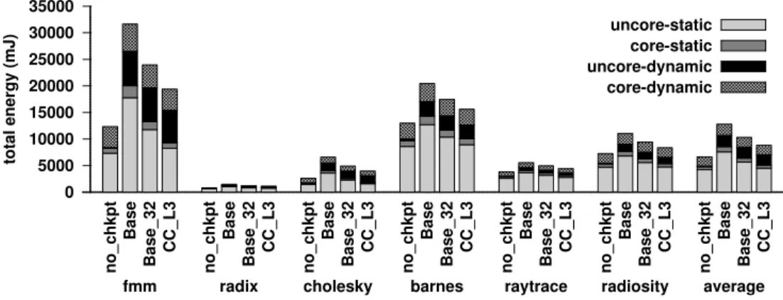
We re-designed several important applications (text processing, databases, checkpoint-ing) to utilize Compute Cache operations. We demonstrate significant speedup (1.9×) and energy savings (2.4×) compared to processors with conventional SIMD units. While our savings for applications are limited by the fraction of their computation that can be ac-celerated using Compute Caches (Amdahl’s law), our micro-benchmarks demonstrate that applications with larger fraction of Compute Cache operations could benefit even more (54×throughput, 9×dynamic energy savings).
1.2
InvisiMem: Smart Memory Defenses for Memory Bus Side
Chan-nel
While performance and energy benefits of NDP have been exploited before in alternate ways, this dissertation also identifies security advantages that NDP can furnish. Privacy concerns is one of the strongest impediment to wider adoption of cloud computing. An
important security concern for trusted cloud computing is the memory bus side channel. An attacker can learn sensitive information about an application by observing data and addresses over the memory bus. While it has received much attention, a low-overhead solution for it is still beyond reach.
Traditional solutions to fix this vulnerability employ the Oblivious RAM (ORAM) [60] construct to hide leaking addresses over the bus. ORAM is a cryptographic construction that obfuscates memory accesses and makes them indistinguishable from a random access pattern. A secure processor can implement ORAM by issuing several memory accesses for every ORAM access. Depending on the size of ORAM, an ORAM access may incur two to three orders of magnitude increase in memory bandwidth and latency compared to a normal DRAM access. In spite of recent advancements [111, 56, 93, 160], even with significant custom hardware support [56], an ORAM-enabled secure processor increases memory ac-cess latency by 20X, which can result in a performance overhead of about 4X. Beside hiding addresses accessed, it is also paramount to hide memory access times, memory ad-dress trace length and provide other security guarantees like data freshness. Providing these additional guarantees only adds to existing severe ORAM overheads.
This dissertation observes that smart memory, memory with compute capability and a packetized interface, can dramatically simplify this problem. Such smart memories are possible today due to recent advancements in 3D integration technology such as the Hybrid Memory Cube (HMC) [12] which make it possible to stack DRAM layers on top of logic layers, and connect them using Through Silicon Via (TSV).
Our proposed solution InvisiMem expands the trust base to include the logic layer in the smart memory to implement cryptographic primitives, which aid in addressing several
memory bus side channel vulnerabilities efficiently. This allows the secure host processor to send encrypted addresses over the untrusted memory bus, and thereby eliminates the need for expensive address obfuscation techniques based on ORAM. Additional measures are required for address confidentiality which we identify and implement efficiently. In ad-dition to address confidentiality, we also discuss how smart memory helps mitigate memory bus timing channel using constant heart-beat packets.
Furthermore, we also observe that smart memory can help reduce the overhead in-curred for guaranteeing data freshness. An adversary tapping the memory bus can rollback the state of a memory block by using older messages. To defeat such replay attacks, the secure processor needs to maintain additional state (version numbers) to ensure that a read response returns the latest version for a memory block ( [152, 56]). With compute capa-bility in memory, InvisiMem establishes a secure channel of communication between the secure processor and memory, such that it guarantees freshness without maintaining such version numbers in the secure host processor.
We demonstrate that InvisiMem designs provide strong defenses against memory bus side channels and efficient data freshness guarantee and have one to two orders of magni-tude of lower overheads for performance, space, energy, and memory bandwidth, compared to prior solutions.
1.3
Sanctuary: Secure and Efficient Memory Management
This dissertation also harnesses NDP to lower the overheads for page fault channel defense. Current state of the art secure processors like Intel SGX (Software Guard
Exten-sions) leave virtual memory management to the operating system. An untrusted operating system can exploit this to induce page faults on every memory access by the application. By doing this, a malicious OS can learn memory access trace of the application at page granularity. A recent work [151] has demonstrated how an application’s page access pat-tern obtained via page-fault side channel can be used to deduce the program path it took during execution which in turn can help deduce the application’s sensitive inputs or outputs. Specifically, they showed how the input image to an image processing application can be completely recovered. This can have catastrophic consequences for privacy of confidential data like medical images which are being processed by cloud services.
Current solutions to fix page fault channel [40] make the unrealistic assumption that all memory needed by an application is reserved a priori. Predetermining application mem-ory requirement is possible by either severely limiting application behavior (no dynamic memory allocations, no recursion etc.) or by reserving large amounts of memory a priori. The latter case can cause information leak if application memory requirement exceeds the reserved memory size during runtime, leading to OS controlled paging activity. Finally, yet importantly, these solutions rob the OS of it’s flexibility in managing memory as a resource; once allocated, memory cannot be reclaimed.
To address the insufficiency of prior works, this dissertation presents Sanctuary, a novel page fault channel defense which unlike prior solutions preserves operating system’s flex-ibility in managing memory as a resource by allowing on-demand page allocations and deallocations. We design a secure runtime which interfaces with the OS on behalf of the application to hide addresses accessed by the application and also secures address transla-tions for sensitive application pages. Our secure runtime uses a novel construct, Oblivious
Page Management (OPAM) which is derived from Oblivious RAM construct [60] but is customized for addressing challenges and exploiting opportunities that arise in the context of page management. The chief source of OPAM overhead comprises of page moves and we perform these page movements near-memory to lower their overheads. Finally, we also propose a novel memory partition which helps reduce the OPAM transactions needed in our system and further brings down the overheads of our solution. We study a suite of cloud applications and show that page fault channel can be fixed at reasonable overheads.
1.4
Organization
The rest of the dissertation is organized as follows. Chapter II presents some back-ground material on near data processing. Chapter III presents Compute Caches which enables computation in caches and delivers performance and energy wins. Chapter IV presents InvisiMem, a secure processor which solves memory bus side channels efficiently using 3D stacked memories. Chapter V discusses an efficient defense against page fault channel vulnerability. Finally, in Chapter VI we conclude the dissertation by summarizing our contributions.
CHAPTER II
Background
In this chapter we look at prior work on Near Data Processing (NDP) paradigm to put the research presented in this proposal in proper context. NDP is a data centric computa-tion paradigm in which computacomputa-tion is moved to where data resides. Prior work on Near Data Processing can be divided into two parts based on whether or not the proposals em-ploy 3D Stacked DRAM. We first present prior work which does not emem-ploy such “smart” memories. We then give a brief background on 3D stacked smart memory followed by proposals which do employ them to harness performance and energy efficiency. Finally, we talk about how the research presented in this proposal breaks new ground in both ex-panding the reach of Near Data Processing and identifying its new advantages which have been hitherto unexplored.
2.1
NDP proposals without 3D Stacked Memory
Traditional DRAM chips have abundant internal bandwidth thanks to large row buffers but only a tiny amount of data per access is shipped to processor (cache block). To solve
this, EXECUBE [86] augments a standard, low cost DRAM chip with logic array compris-ing of eight processors and interface ports. Each such processor can either work indepen-dently or in tandem with other processors in a SIMD fashion. Such processors then enjoy far more memory bandwidth than traditional systems which connect to off-chip memory via memory bus.
Terasys [58] transforms conventional memory into a SIMD processor array. In this proposal, a traditional SRAM array can either support normal read/write mode or a spe-cial PIM (processing in memory) mode. In PIM mode, processors associated with each column in SRAM array perform a specific command on a selected row in SRAM array. The processors present are bit serial that access and process bits from attached memory. Each cycle, the processors can either load or store data and perform computation on data using an ALU. Terasys also provides some reduction capabilities on the results produced by these processors such as combining results of all processors to send a single bit result to host processor.
IRAM [106] proposes unifying DRAM and logic into single DRAM chip in response to growing processor-memory performance gap. Such an organization can utilize internal DRAM bandwidth better as compared to traditional processor memory configuration. As memory is now effectively on-chip, memory latency is lower. Furthermore, energy ex-pended is lower too as far more memory is available on-chip than would be possible using SRAM as DRAM is far denser.
Active Pages [102] proposes partitioning applications between traditional processor and intelligent memory system such that data intensive parts of the application are carried out by the memory. “Active pages” consists of a page of data and functions which manipulate the
data. The memory system employed is capable of both storing the data and performing the data manipulations. This proposal implements memory system managing “active pages” using re-configurable architecture DRAM which integrates FPGA and DRAM technology. FlexRAM [77] models memory flexibly as either default DRAM chip or a PIM (pro-cessing in memory) chip which performs computation. This proposal models PIM chips based on Merged Logic DRAM (MLD) process which integrates logic and DRAM in a sin-gle chip. PIM chips consist of simple processing elements finely interleaved with DRAM cells which have high bandwidth access to memory. A low-issue superscalar RISC core is also modeled in each PIM chip to co-ordinate the processing of the simple processing elements without relying on host processor.
DIVA [49] or Data IntensiVe Architecture models PIM chips (memory with processing logic) as co-processors for a conventional system which can either be used to perform computation close to memory or be used as traditional DRAM chips. Each DIVA PIM chip is a memory device augmented with a processor and communication hardware for PIM chips to interact with each other. Form of active messages called “parcels” are used to communicate computation and synchronize PIM chips. DIVA memory is partitioned between that accessible to host processor only, PIM chips only and global memory that is accessible to both. DIVA also enables light weight address translations on PIM chips using segments.
While all prior proposals aim to add logic to memory to support general purpose pro-grams, Intelligent Memory Manager [112] augments memory with a simple processor which solely aims to aid the host processor by performing memory management func-tions (prefetching of data, relocation of data) on its behalf. Such funcfunc-tions typically tend to
pollute processor caches. By performing them using processor in memory, such pollution can be avoided.
2.2
3D Stacked Memory
Advancements in 3D integration have made possible 3D Stacked memories which are now commercially available [16]. A typical 3D Stacked memory consists of several layers of DRAM dies stacked on top of each other, with a logic layer at the bottom. The DRAM banks are organized into sets of independent vaults, and the various layers are connected using Through Silicon Vias (TSVs) [12]. High density, short length TSVs in conjunction with vaults which function independently and can be accessed in parallel are the chief sources of high bandwidth provided by such a system.
Two of the most popular 3D stacked designs present are HMC [12] and HBM [83]. Both of them employ multiple memory dies stacked together with a logic die at the base. HMC places memory controller logic in the logic die. While their internal implementations differ, most importantly, how they are integrated with the main host processor also differs. In case of HMC an high speed packet based serial interface connects it to the CPU. In case of HBM however, interaction with CPU is achieved using another silicon layer, termed silicon interposer.
2.2.1 NDP proposals with 3D Stacked Memory
Several proposals employ such 3D Stacked memories to harness performance for var-ious applications. Pugsleyet al. [109] model several simple processing cores in the logic
layer of 3D Stacked memory which perform the Map operation to accelerate MapReduce workloads. In TOP-PIM [159], the authors model GPU in logic layer of 3D Stacked mem-ory and study several GPGPU workloads to identify characteristics that make workloads amenable to be offloaded to GPU near memory. Ahnet al.[22] proposed a locality aware PIM design, which opportunistically decides when computation should be offloaded to memory and when it should be performed using host processor instructions.
2.3
Breaking New Ground in NDP
All prior proposals augment the main memory to play an active part in computation. For applications with no cache locality, compute capable memory is clearly an effective solution. But for cache friendly applications, always computing in memory may not be an efficient choice. However, the other extreme of computing the traditional way, as this pro-posal shows, incurs high instruction processing overheads and expends significant energy for moving data over memory hierarchy.
To address these limitations, this proposal introduces a new way to realize near-data computing by enabling processor caches to perform computation. Using our proposed solution, caches can perform simple operations common to wide variety of applications. Using our system, data can be moved to the cache level most suitable to it’s reuse profile.
Most near-data processing proposals presented in this chapter seek to attain perfor-mance and energy gains. Our proposal also identifies and exploits an hitherto untapped advantage of NDP to provide low-overhead security guarantees.
CHAPTER III
Compute Caches: Caches that Compute
This chapter presents Compute Caches, our novel proposal to enable computations in processor caches. With Compute Caches we add a new technique to exploit the near data processing paradigm. Compute centric architectures employ processor caches merely to stage data and they otherwise play no active role in computation. However, with Compute Caches, processor caches can now play an active and a powerful role in computation. Com-pute Caches not only provide advantages of vector processing but also help avoid excessive data movement over memory hierarchy.
3.1
Introduction
As computing today is dominated by data-centric applications, there is a strong impetus for specialization for this important domain. Conventional processors’ narrow vector units fail to exploit the high degree ofdata-parallelismin these applications. Also, they expend disproportionately large fraction of time and energy in moving dataover cache hierarchy, and in instruction processing, as compared to the actual computation [41].
We present the Compute Cache architecture for dramatically reducing these inefficien-cies through in-place (in-situ) processing in caches. A modern processor devotes a large fraction (40-60%) of die area to caches which are used for storing and retrieving data. Our key idea is to re-purpose and transform the elements used in caches into active computa-tional units. This enables computation in-place within a cache sub-array, without transfer-ring data in or out of it. Such a transformation can unlock massive data-parallel compute capabilities, dramatically reduce energy spent in data movement over the cache hierarchy, and thereby directly address the needs of data-centric applications.
Our proposed architecture uses an emerging SRAM circuit technology, which we refer to as bit-line computing [73, 76]. By simultaneously activating multiple word-lines, and sensing the resulting voltage over the shared bit-lines, several important operations over the data stored in the activated bit-cells can be accomplished without data corruption. A recently fabricated chip [73] demonstrates feasibility of bit-line computing. They also show a stability of more than six sigma robustness for Monte Carlo simulations, which is considered industry standard for robustness against process variations.
Past processing-in-memory (PIM) solutions proposed to move processing logic near the cache [87, 50] or main memory [107, 126]. 3D stacking can make this possible [22]. Compute Caches significantly push the envelope by enabling in-place processing using existing cache elements. It is an effective optimization for data-centric applications, where at least one of the operands (e.g., dictionary in WordCount) used in computation has cache locality.
Efficiency of Compute Caches arises from two main sources: massive parallelism and reduced data movement. A cache is typically organized as a set of sub-arrays; as many
as hundreds of sub-arrays, depending on the cache level. These sub-arrays can potentially compute concurrently on data stored in them (KBs of data) with little extensions to the ex-isting cache structures (8% of cache area overhead). Thus, caches can effectively function as large vector computational units, whose operand sizes are orders of magnitude larger than conventional SIMD units (KBs vs bytes). To achieve similar capability, the logic close to memory in a conventional PIM solution would need to provision more than hun-dred additional vector functional units. The second benefit of Compute Caches is that they avoid the energy and performance cost incurred not only for transferring data between the cores and different levels of cache hierarchy (through network-on-chip), but even between a cache’s sub-array to its controller (through in-cache interconnect).
We address several problems in realizing the Compute Cache architecture, discuss ISA and system software extensions, and re-designs several data-centric applications to take advantage of the new processing capability.
An important problem in using Compute Caches is satisfying theoperand locality con-straint. Bit-line computing requires that the data operands are stored in rows that share the same set of bit-lines. We architect a cache geometry, where ways in a set are judiciously mapped to a sub-array, so that software can easily satisfy operand locality. Our design al-lows a compiler to ensure operand locality simply by placing operands at addresses that are page aligned (same page offset). It avoids exposing the internals of a cache, such as its size or geometry, to software.
When in-place processing is not possible for an operation due to lack of operand lo-cality, we propose to use near-place Compute Caches. In near-place design, the source operands are read out from the cache sub-arrays, the operation is performed in a logic unit
placed close to the cache controller, and the result may be written back to the cache. Besides operand locality, Compute Caches brings forth several interesting questions. How to orchestrate concurrent computation over operands spreading across multiple cache sub-arrays? How to ensure coherence between compute-enabled caches? How to ensure consistency model constraints when computation is spread between cores and caches? Soft errors are a significant concern in modern processors. Can Error Correction Codes (ECC) be used for Compute Caches? When not possible, what are the alternative solutions? We discuss relatively simple solutions to address these problems.
Compute Caches support several in-place vector operations: copy, search, compare and logical operations (and, or,xor, and not) which can accelerate a wide variety of applica-tions. We study two text processing applications (word count, string matching), database query processing with bitmap indexing, copy-on-write checkpointing in OS, and bit matrix multiplication (BMM); a critical primitive used in cryptography, bioinformatics, and image processing. We re-designed these applications to efficiently represent their computation in terms of Compute Cache supported vector operations. Section 3.5 identifies a number of additional domains that can benefit from Compute Caches: data analytics, search, network processing etc.
We evaluate the merits of Compute Caches for a multi-core processor modeled after Intel’s SandyBridge [88] processor with eight cores, three levels of caches, and a ring inter-connect. For the applications we study, on average, Compute Caches improve performance by 1.9× and reduce energy by 2.4× compared to a conventional processor with 32-byte wide vector units. Applications with a higher fraction of Compute Cache operations can benefit significantly more. Through micro-benchmarks that manipulate 4KB operands, we
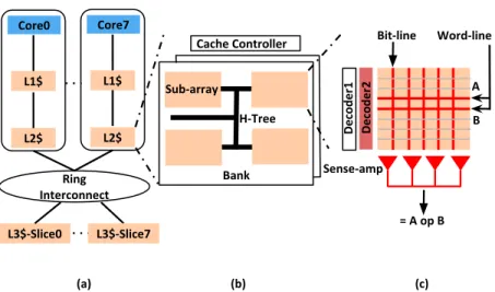
Core0 L1$ L2$ Ring Interconnect L3$-Slice0 H-Tree Sub-array Bank Cache Controller L3$-Slice7 Sense-amp Word-line Core7 L1$ L2$ Bit-line = A op B A B Decoder1 Decoder2 (a) (b) (c)
Figure 3.1: Compute Cache overview. (a) Cache hierarchy. (b) Cache geometry (c) In-place compute in a sub-array.
show that Compute Caches provide 9×dynamic energy savings over a baseline using 32-byte SIMD units while providing 54×better throughput on average.
3.2
Background
This section provides a brief background of cache hierarchy, cache geometry, and bit-line computing in SRAM.
3.2.1 Cache Hierarchy and Geometry
Figure 3.1 (a) illustrates a multi-core processor modeled loosely after Intel’s Sandy-bridge [88]. It has a three-level cache hierarchy comprising of private L1 and L2, and a shared L3. The shared L3 cache is distributed into slices which are connected to the cores via a shared ring interconnect. A cache consists of a cache controller and several banks ((Figure 3.1 (b)). Each bank has several sub-arrays connected by a H-Tree interconnect. For example, a 2 MB L3 cache slice has a total of 64 sub-arrays distributed across 16 banks. A sub-array in a cache bank is organized into multiple rows of data-storing bit-cells.
BLB0 BL0 Vref WLi WLj SA SA SA SA 0 1 0 1 0 1 1 0 BLBn BLn
WLiNORWLj WLiANDWLj
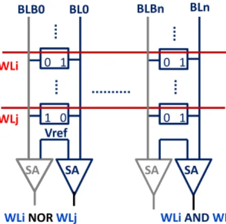
Figure 3.2: SRAM circuit for in-place operations. Two rows (WLi and WLj) are activated. AnANDoperation is performed by sensing bit-line (BL). All the bit-lines are initially pre-charged to ‘1’. If both the activated bits in a column have a ‘1’ (column ‘n’), then the BL stays high and it is sensed as a ‘1’. If any one of the bits were ‘0’ it will lower the BL voltage below Vref and will be sensed as a ‘0’. A NOR operation can be performed by sensing bit-line bar (BLB).
The bit-cells in the same row are connected to a word-line. The bit-cells along a column share the same bit-line. Typically, in any cycle, one word-line is activated, from where a data block is either read from, or written to, through the column bit-lines.
3.2.2 Bit-line Computing
Compute Caches use emerging bit-line computing technology in SRAMs [73, 76] (Fig-ure 3.2) which observes that, when multiple word-lines are activated simultaneously, the shared bit-lines can be sensed to produce the result ofand andnoron the data stored in the two activated rows. Data corruption due to multi-row access is prevented by lower-ing word-line voltage to bias against write of the SRAM array. Jeloka et al. [73]’s mea-surements across 20 fabricated test chips demonstrate that data-corruption does not occur even when 64 word-lines are simultaneously activated during such an in-place computa-tion. They show a stability of more than six sigma robustness for Monte Carlo simulations, which is considered industry standard for robustness against process variations. Also, note
core alu data-mov
Cache
Core Core
(a) Scalar Core
Cache Cache
(b) SIMD Core (c) Compute Cache Core
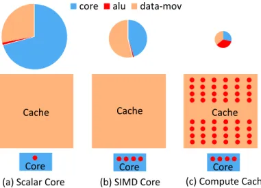
Figure 3.3: Proportion of energy (top) for bulk comparison operation and area (bottom). Red dot depicts logic capability.
that, by lowering the word-line voltage further, robustness can be improved at the cost of increase in delay. Even with it, Compute Caches will still deliver significant savings given its potential (Section 3.6, 54×throughput, 9×dynamic energy savings).
Section 3.4.2 discusses our extensions to bit-line computing enabled SRAM to support additional operations: copy, xor, equality comparison, search, and carryless multiplica-tion (clmul).
3.3
A Case for Compute Caches
In-place Compute Cache has the potential to provide massive data-parallelism, while also dramatically reducing the instruction processing and on-chip data movement over-heads. Figure 3.3 pictorially depicts these benefits by comparing a scalar core, a SIMD core with vector processing support, and Compute Caches.
The bottom half in Figure 3.3 depicts the area proportioning and processing capability of the three architectures. Significant fraction of die area in a conventional processor is for
Cache cache-ic (h-tree) cache-access
L1-D 179 pJ 116 pJ
L2 675 pJ 127 pJ
L3-slice 1985 pJ 467 pJ
Table 3.1: Cache energy per read access
caches. A Compute Cache re-purposes the elements used in this large area into compute units for a small area overhead (8% of cache area). A typical last-level cache consists of hundreds of sub-arrays distributed across different banks which can potentially compute concurrently on cache blocks stored in them. This enables us to exploit large scale data level parallelism (e.g. a 16MB L3 has 512 sub-arrays and can support 8 KB operands) dwarfing even a SIMD core.
The top row of Figure 3.3 shows relative energy consumption for a comparison op-eration over several blocks of 4KB operands (Section 3.6.4). In a scalar core, less than 1% of the energy is expended on the ALU operation, while nearly three quarters of the energy is spent in processing instructions in the core, and one-fourth is spent on data move-ment. While vector processing (SIMD) support (Figure 3.3 (b)) in general-purpose and data-parallel accelerators reduce the instruction processing overhead to some degree, it does not help address the data movement overhead. Compute Cache architecture (Fig-ure 3.3 (c)) can reduce the instruction processing overheads by an order of magnitude, by supporting SIMD operation on large operands (tens of KB). Also, it avoids the energy and performance cost due to data movement.
In-place Compute Cache reduces on-chipdata movement overhead, which consists of two components. First, is the energy spent on data transfer. This includes not only the significant energy spent on the processor interconnect’s wires and routers, but also the
H-Tree interconnect used for data transfer within a cache. A near-place Compute Cache solution can solve the former but not the latter. As shown in Table 3.1, H-Tree consumes nearly 80% of cache energy spent in reading from a 2MB L3 cache slice.
Second, is the energy spent when reading and writing in the higher-level caches. In a conventional processor, a data block trickles up the cache hierarchy all the way from L3 to L1 cache, and into a core’s registers, before it can be operated upon. An L3 Compute Cache can eliminate all this overhead. A shared L3 Compute Cache can also reduce the cost of sharing data between two cores, as it would avoid write-back from a source core’s L1 to shared L3, and then a transfer back to a destination core’s L1.
3.4
Compute Cache Architecture
Figure 3.1 illustrates the Compute Cache (CC) architecture. We enhance all the levels in the cache hierarchy with in-place compute capability. Computation is done at the highest level where the application exhibits significant locality. In-place compute is based on the bit-line computing technology we discussed in Section 3.2. We enhance these basic in-place compute capabilities to support xor and several in-place operations (copy, search, comparison, and carryless multiplication).
In-place computing is possible only when operands are mapped to sub-arrays such that they share the same bit-lines. We refer to this requirement as operand locality. We discuss a cache geometry that allows a compiler to satisfy operand locality by ensuring that the operands are page-aligned.
Opcode Src1 Src2 Dest Size Description cc copy a - b n b[i] =a[i] cc buz a - - n a[i] = 0 cc cmp a b r n r[i] = (a[i] ==b[i]) cc search a k r n r[i] = (a[i] ==k) cc and a b c n c[i] =a[i] &b[i] cc or a b c n c[i] = (a[i]||b[i]) cc xor a b c n c[i] =a[i]⊕b[i] cc clmulX a k c n ci =⊕(a[i] &k) cc not a - b n b[i] =!(a[i])
a,b,c,k: addresses r:register ∀i, i∈[1, n], X = [ 64/128/256 ]
Table 3.2: Compute Cache ISA.
across its several banks. It also decides the cache level to perform the computation and fetches the operands to that level. Given that a Compute Cache can modify data, we discuss its implication in ensuring coherence and consistency properties. Finally, we discuss design alternatives for supporting ECC in Compute Caches.
In the absence of operand locality, we propose to compute near-place in cache. For this, we add a Logic Unit in the cache controller. Although near-place cache computing requires additional functional units, and cannot save H-Tree interconnect energy inside caches, it successfully helps reduce the energy spent in transferring and storing data in the higher-level caches.
3.4.1 Instruction Set Architecture (ISA)
Compute Cache (CC) ISA extensions are listed in Table 3.2. It supports several vector instructions, whose operands are specified using register indirect addressing. Operand sizes are specified through immediate values and can be as large as 16K. It supports vector copy-ing, zerocopy-ing, and logical operations. It also supports vector carry less multiply instruction (cc clmul) at single/double/quad word granularity. It also supports equality comparison
and search. We limit the operand size (n) of these instructions to 64 words (512 bytes), so that the result can be returned as a 64-bit value to a processor core’s register. For the search instruction, the key size is set to 64 bytes. For smaller keys, the programmer can either duplicate the key multiple times starting from the key’s address (if its size is a word multiple), or pad the key and source data operands to be 64 bytes.
3.4.2 Cache Sub-arrays with In-Place Compute
BLB0 BL0 Vref WLi WLj SA SA SA SA 0 1 0 1 1 0 0 1 BLBn BLn Destination Enabled Copy_Wr Enable Wr_Enable D0 Db0 Dn Dbn 0 1 0 1 0 1 0 1
Figure 3.4: In-place copy operation (from row i to j).
Compute Caches is made possible by our SRAM sub-array design that facilitates in-place computation. We start with the basic circuit framework proposed by Jelokaet al.[73], which supports logicaland andnoroperations. To a conventional cache’s sub-array, we add an additional decoder to allow activating two wordlines, one for each operand. The two single-ended sense amplifiers required for separately sensing both the bit-lines attached to a bit-cell are obtained by re-configuring the original differential sense amplifier.
In addition toandandnoroperations, we extend the circuit to supportxoroperation by NOR-ing bit-line and bit-line complement. We realize compound operations such as
compare and search by using the results of bitwise xor. To compare two words, the individual bit-wisexor results are combined using a wired-NOR. Comparison is utilized to do iterativesearchover cache blocks stored in sub-arrays.
By feeding the result of the sense-amplifiers back to the bit-lines, one word-line can be copied to another without ever latching the source operand. We leverage the fact that the last read value is same as the data to be written in the next cycle, and coalesce the read-write operation to enable more energy-efficientcopyoperation as shown in Figure 3.4. By resetting input data latch before a write we can enable in-place zeroing of a cache block.
Finally, the carryless multiplication (clmul) operation is done using a logicalandon two sub-array rows, followed byxorreduction of all the resultant bits. This is supported by adding axorreduction tree to each sub-array.
Our extensions have negligible impact on the baseline read/write accesses as they use the same circuit as the baseline, including differential sensing. An in-place operation takes longer than a single read or write sub-array access, as it requires longer word-line pulse to activate and sense two rows to compensate for the lower word-line voltage. Sensing time also increases due to the use of single-ended sense amplifiers, as opposed to differential sensing. However, note that this is still less than the delay baseline would incur to accom-plish an equivalent in-place operation, as it would require multiple read accesses and/or write access. Section 3.6.3 provides the detailed delay, energy and area parameters for compute capable cache sub-arrays.
3.4.3 Operand Locality
For in-place operations, the operands need to be physically stored in a sub-array, such that they share the same set of bitlines. We term this requirement as operand locality. In this section, we discuss cache organization and software constraints that can together satisfy this property.Fortunately, we find that software can ensure operand locality as long as operands are page-aligned, i.e., have the same page offset. Besides this, the programmer
or the compiler does not need to know about any other specifics of the cache geometry.
Bank H-Tree
Sub-array
Cache {1 bank, 16 sets (S0-S15), 4 ways per set}
Bank Bits Physical Address Decoding Way 0 S0 S2 BP0 BP1 S4 BP2 BP3 BP4 BP5 BP6 BP7 Block Partition S1 (b) (a) S5 S6 S7 S12 S13 S14 S15 S8 S9 S10 S11 Way 1 Way 2 Way 3 S3 Block offset Set index Tag
Figure 3.5: Cache organization example, address decoding ([i][j] = set i, way j), alternate address decoding for parallel tag-data access caches
Operand locality aware cache organization: Figure 3.5 illustrates a simple cache with one bank each with four sub-arrays. Rows in a sub-array share the same set of bitlines. We define a new term,Block Partition(BP). Block partition for a sub-array is the group of cache blocks in that sub-array that share the same bitlines. In-place operation is possible between any two cache blocks stored within a block partition. In our example, since each row in a sub-array has two cache blocks, there are two block partitions per sub-array. In
total, there are eight block partitions (BP0-BP7). In-place compute is possible between any blocks that map to the same block partition ( e.g. blocks in setsS0andS2).
We make two design choices for our cache organization to simplify operand locality constraint. First, all the ways in a set are mapped to the same block partition as shown in Figure 3.5(a). This ensures that operand locality would not be affected based on which way is chosen for a cache block.
Second, we use a portion of set-index bits to select the block’s bank and block parti-tion, as shown in Figure 3.5(b). As long as these are the same for two operands, they are guaranteed to be mapped to the same block partition.
Software requirement: The number of address bits that must match for operand lo-cality varies based on the cache size. As shown in Table 3.3, even the largest cache (L3) in our model requires that only least 12 bits are the same for two operands (we assume pages are mapped to a NUCA slice closest to the core actively accessing them). Given that our pages are 4KB in size, we observe that as long as the operands are page aligned, i.e., have the same page offset, then they will be placed in the address space such that the least sig-nificant bits (12 for 4 KB page) in their addresses (both virtual and physical) match. This would trivially satisfy the operand locality requirement for all the cache levels and sizes we study. Note that, we only require operands to be placed at the same offset of 4KB mem-ory regions, and it is not necessary to place them in separate pages. For super-pages that are larger than 4KB, operands can be placed within a page while ensuring 12-bit address alignment.
We expect that for data-intensive regular applications that operate on large chunks of data, it is possible to satisfy this property. Many operating system operations that involve
Cache Banks BP Block size Min. address bits match
L1-D 2 2 64 8
L2 8 2 64 10
L3-slice 16 4 64 12
Table 3.3: Cache geometry and operand locality constraint.
copying from one page to another are guaranteed to exhibit operand locality for our system. Compiler and dynamic memory allocators could be extended to optimize for this property in future.
Finally, a binary compiled with a given address bit alignment requirement (12 bits in our work) is portable across a wide range of cache architectures as long as the number of address bits to be aligned is equal to or less than what they were compiled for. If the cache geometry changes such that it requires greater alignment, then the programs would have to be recompiled to satisfy that stricter constraint.
Column Multiplexing: With column multiplexing, multiple adjacent bit-lines are mul-tiplexed to a single bit data output, which is then observed using one sense-amplifier. This keeps area overhead of peripherals under check and improves resilience to particle strikes. Fortunately, in column multiplexed sub-arrays, adjacent bits in a cache block are inter-leaved across different sub-arrays such that their bitlines are not multiplexed. In this case, the logical block partition that we defined would be interleaved across the sub-arrays. Thus, an entire cache block can be accessed in parallel. Given this, in-place concurrent operation on all the bits in a cache block is possible even with column multiplexing.
Our design choice of placing ways of a set within a block partition does not affect the degree of column multiplexing as we interleave cache blocks of different sets instead.
within a block partition, so that operand locality is not dependent on which way is chosen for a block at runtime. However, this prevents us from supporting parallel tag-data access, where all the cache blocks in a set are pro-actively read in parallel with the tag match. This optimization is typically used for L1 as it can reduce the read latency by overlapping tag match with read. But it incurs a high read energy overhead (4.7× higher energy per access for L1 cache) for modest performance gain (2.5% for SPLASH-2[147]). Given the significant benefits of L1 Compute Cache, we think it is a worthy trade-off to forgo this optimization for L1.
3.4.4 Managing Parallelism
Cache controllers are extended to provision for CC controllers which orchestrate the execution of CC instructions. The CC controller breaks a CC instruction into multiple simple vector operations whose operands span at most a single cache block and issues them to the sub-arrays. Since a typical cache hierarchy can have hundreds of sub-arrays (16MB L3 cache has 512 sub-arrays), we can potentially issue hundreds of concurrent operations. This is only limited by two factors. First, the bandwidth of the shared interconnects used to transmit address/commands. Note that we do not replicate the address bus in our H-tree interconnects. Second, number of sub-arrays activated at same time can be limited to limit peak power drawn.
The controller at L1-cache uses aninstruction tableto keep track of the pend-ing CC instructions. The simple vector operations are kept track of in the operation table. The instruction table tracks metadata associated at instruction level (i.e., result, count of simple vector operations completed, next simple vector operation to be
gener-ated). The operation table, on other hand, tracks status of each operand associated with the operation and issues request to fetch the operand if it is not present in the cache (Sec-tion 3.4.5). When all operands are in cache, we issue the opera(Sec-tion to the cache sub-array. As operations complete they update the instruction table, and the L1-cache controller noti-fies the core when an instruction is complete.
To support search instruction, CC controller replicates key in all the block partitions where the source data resides. To avoid doing this again for the same instruction, we track such replications per instruction in akey table.
Finally, if the address range of any operand of a CC instruction spans multiple pages, it raises a pipeline exception. The exception handler splits the instruction into multiple CC operations such that each of its operands are within a page.
3.4.5 Fetching In-Place Operands
The Compute Cache (CC) controllers are responsible for deciding the level in the cache hierarchy where CC operations need to be performed, and issuing commands to the cache sub-array to execute them. To simplify our design, in our study, the CC controller always performs the operations at the highest-level cache whereall the operands are present. If any of the operands are not cached, then the operation is performed at lowest-level cache (L3). Cache allocation policy can be improved in future by enhancing our CC controller with a cache block reuse predictor [70].
Once a cache level is picked, CC controller fetches any missing operands to that level. The controller also pins the cache-lines the operands are fetched in while the CC operation is under way. To avoid the eviction of operands while waiting for missing operands, we
CORE free free free B : dirty A : clean free L1
1. Core issues cc_and
to L1 controller
L2
2. L1 forwards operation to L2
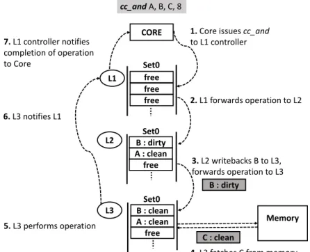
4. L3 fetches C from memory B : clean A : clean free L3 3. L2 writebacks B to L3, forwards operation to L3 cc_and A, B, C, 8 5. L3 performs operation 6. L3 notifies L1 7. L1 controller notifies completion of operation to Core Memory C : clean Set0 Set0 Set0 B : dirty
Figure 3.6: Compute Caches in action
promote the cache blocks of that operand to the MRU position in the LRU chain. However, on receiving a forwarded coherence request, we release the lock to avoid deadlock and re-fetch the operand. Getting a forwarded request to a locked cache line will be rare for two reasons. First, in DRF [20] compliant programs, only one thread will be able to operate on a cache block while holding its software lock. Second, as operands of a single CC operation are cache block wide, false sharing will be low. Nevertheless, to avoid starvation in pathological scenarios, if CC operation fails to get permission after repeated attempts (set to two), processor core will translate and execute a CC operation as RISC operations.
Figure 3.6 shows a working example. Core issues operation cc and with address operands A, B and C to L1 controller ( 1). Each is of size 64 bytes (8 words) spanning an entire cache block. For clarity, only one cache set in each cache level is shown. None of the operands are present in L1 cache. Operand B is in L2 cache and is dirty. L3 cache has
clean copy of A and a stale copy of B. C is not in any cache.
L3 cache is chosen for the CC operation, as it is the highest cache level where all operands are present. L1 and L2 controllers will forward this operation to L3 (2, 3 ). Before doing so, L2 cache will first back B to L3. Note that caches already write-back dirty data to next cache level on eviction and we use this existing mechanism.
On receiving the command, L3 fetches C from memory (4 ). Note that, as an optimiza-tion, C need not be fetched from memory as it will be over-written entirely. Once all the operands are ready, L3 performs the CC operation ( 5 ) and subsequently notifies the L1 controller ( 6) of it’s completion, which in turn notifies the core ( 7).
3.4.6 Cache Coherence
Compute Cache optimization interacts with the cache coherence protocol minimally and as a result does not introduce any new race conditions. As discussed above, while the controller locks cache lines while performing CC operation, on receipt of a forwarded coherence request, the controller releases the lock and responds to the request. Thus, a forwarded coherence request is always responded to in cases where it would be responded to in the baseline design.
Typically, higher-level caches writeback dirty data to the next-level cache on evictions. Coherence protocols already support such writebacks. In the Compute Cache architecture, when a cache level is skipped to perform CC operations, any dirty operands in the skipped level need to be written back to next level of cache to ensure correctness. To do this, we use the existing writeback mechanism and thus require no change to the underlying coherence protocol.
3.4.7 Consistency Model Implications
Current language consistency models (C++ and Java) are variants of the DRF model [20], and therefore a processor only needs to adhere to the RMO memory model. While ISAs providing stronger guarantees (x86) exist, they can be exploited only by writing assem-bly programs. As a consequence, while we believe stronger memory model guarantees for Compute Caches is an interesting problem (to be explored in future work), we assume RMO model in our design. In RMO, no memory ordering is needed between data reads and writes, including all CC operations. Individual operations within a vector CC instruction can also be performed in parallel by the CC controller.
Programmers usefenceinstructions to order memory operations, which is sufficient in the presence of CC instructions. Processor stalls commit of a fence operation until pre-ceding pending operations are completed, including CC operations. Similar to conventional vector instructions, it is not possible to specify a fence between scalar operations within a single vector CC instruction.
3.4.8 Memory Disambiguation and Store Coalescing
Similar to SIMD instructions, Compute Cache (CC) vector instructions require addi-tional support in the processor core for memory ordering. We classify instructions in CC ISA into two types. CC-R type (cc cmp, cc search) only read from memory. The rest of the instructions are CC-RW type as they both read and write from memory. Under RMO memory model, CC-R can be executed out-of-order, whereas CC-RW behaves like a store. In the following discussion, we refer to CC-R as load, and CC-RW as store.
Conventional processor cores use a load-store queue (LSQ) to check for address con-flicts between a load and the preceding uncommitted stores. As vector instructions can access more than a word, it is necessary to enhance the LSQ with the support for checking address ranges, instead of just one address. For this reason, we use a dedicated vector LSQ, where each entry has additional space to keep track of address ranges for the operands of a vector instruction.
Similar to LSQ, we also split the store buffer into two, one for scalar stores and an-other for vector stores. The vector store buffer supports address range checks (max 12 comparisons/entry). Our scalar store buffer permits coalescing. However, it is not possible to coalesce CC-RW instructions with any store, because their output is not known till they are performed in a cache. As the vector store buffer is non-coalescing, it is possible for the two store buffers to contain stores to the same location. If such a scenario is detected, the conflicting store is stalled until the preceding store is complete which ensures program order between stores to the same location. We augment the store buffer with a field which points to any successor store and a stall bit. The stall bit is reset when the predecessor store completes.
Data values are not forwarded from vector stores to any loads, or from any store to a vector load. Code segments where both vector and scalar operations access the same location within a short time span is likely to be rare. If such a code segment is frequently executed, the compiler can choose to not employ Compute Cache optimization.
![Figure 3.5: Cache organization example, address decoding ([i][j] = set i, way j), alternate address decoding for parallel tag-data access caches](https://thumb-us.123doks.com/thumbv2/123dok_us/10226256.2926467/40.918.246.736.435.728/figure-organization-example-address-decoding-alternate-decoding-parallel.webp)