Technology (IJRASET)
Implementation of Sub-Threshold Source
Coupled Logic for Ultra-Low Power Application
B.V.Ramana#1, S.Md.Imran Ali#2, P.Nagashyam#3, Y.Sandeep*4, Sudharshan#5
#12345
BITS, Electronics and Communication Engineering, JNTUA
Abstract— This thesis work generally focuses on the use of sub-threshold source combined logic (STSCL) for building digital circuits and systems working at very low voltage and promise to provide desirable performance with excellent energy savings. Industries like bio-engineering and smart sensors require the energy consumption to be effectively very low for long battery life. Alongside interacting with the ultra-low power requirements, the device must also be reliable, robust, and perform well under harsh conditions. In this thesis work, logic gates are designed and analysed, using STSCL. These gates are further used for implementation of digital subsystems in small-sized smart dust sensors which would operate at very low supply voltages and consume extremely low electricity.
The simulated results are studied, analysed and as opposed with same CMOS-based digital circuits. The results show on the good thing about STSCL-based digital systems over CMOS.
Keywords— CMOS, STSCL, Sub-threshold,
I. INTRODUCTION
Ultra-low electricity requirements have become obligatory in many aspects of digital circuits and systems. The demands are incredibly full of app fields, such as bio-engineering and smart sensors. Attaining low power dissipation includes minimization of the entire seapage current. For a CMOS logic gate, the main concerns with respect to leakage are static management (due to gate-to-channel tunneling and sub-threshold off-state leakage) and dynamic dissipation. Pertaining to process technologies above sixty five nm, the dissipation credited to static leakage is comparatively negligible regarding active power, but as technology scales down to forty-five nm and below, the static leakage exhibits bigger impacts on the overall power consumption of CMOS logic.
Thus this work studies the source combined logic (SCL) and seeks at using it for implementation, in replacement of CMOS, for conventional digital systems to identify and observe any features of this differential form of reason over CMOS. This work thereby attempts to find whether an improved low electric power configuration can be performed for conventional systems without the enhancements, just by jogging source coupled logic at sub-threshold region.
Source coupled reasoning (SCL), operating in the sub-threshold region, is analyzed and analyzed in this work along with CMOS logic to see the good thing about having lower fixed and dynamic leakage management for 65 nm and 45 nm MOS. The SCL style is a dual-rail differential logic style and has an additional routing complexity due to its dual rail feature, but provides noise protection and twice the indicate output swing when compared with CMOS logic. Now, operating the SCL logic in the sub-threshold region permits the option to run the gates at low source voltage, down to zero. 2 V, since current density for sub limit procedure is really small for SIMPLY devices. Allowing the way power dissipation to be very low as the dynamic power is quadratic ally proportional to the supply voltage in line with the popular formula
Pdynamic = α.f.c.v2
II. LITERATURESURVEY
CMOS is also sometimes termed as complementary-symmetry metal-oxide-semiconductor (or COS-MOS). The words "complementary-symmetry" refer to the fact that the standard design style with CMOS uses complementary and symmetrical pairs of p-type and n-type metal oxide semiconductor field effect transistors (MOSFETs) for logic functions.
Two important characteristics of CMOS devices are high noises immunity and low stationary power consumption.[3] Since one transistor of the pair is actually off, the series combo takes in significant power only briefly during switching between on and off states. As a result, CMOS devices do not produce as much waste products heat as other varieties of logic, for example transistor-transistor logic (TTL) or NMOS logic, which normally have some standing current even when not changing condition. CMOS also allows a top density of logic functions on a chip. That was generally forthis reason that CMOS became the most used technology to be implemented in VLSI chips.
Technology (IJRASET)
from another PMOS diffusion. Similarly, all NMOS diffusion must have either an input from ground or from another NMOS receptor. The composition of a PMOS transistor creates low resistance between its source and drain contacts when a low gate volts is applied and high resistance if a high door voltage is applied. Upon the other hand, the composition of an NMOS transistor creates high level of resistance between source and drain when a low gateway voltage is applied and low resistance every time a high gate voltage is applied. CMOS accomplishes current lowering by complementing every nMOSFET with a pMOSFET and connecting both gates and both drains together. A high voltage on the gates will cause the nMOSFET to conduct and the pMOSFET to not conduct, while a low voltage on the entrance causes the reverse. This kind of arrangement greatly reduces ability consumption and heat technology. However, during the turning time, both MOSFETs do briefly as the gateway voltage goes from one state to another. This kind of induces a brief increase in power consumption and turns into a serious issue at highs Attributes of CMOS logic:
A. Dissipates low power: The ability waste is dependent on the ability supply voltage, frequency, outcome load, and input climb time. At 1 Megahertz and 50 pF weight, the power dissipation is typically 10 nW every gate.
B. Short propagation holdups hindrances impediments: Depending on the ability, the propagation delays are usually around 25 natursekt to 50 nS..
C. Noise immunity approaches 50 percent or 45% of the full logic swing.
D. Levels of the logic indication will be essentially similar to the power delivered since the input impedance is so high.
Domino CMOS logic provides higher velocity and easier testability in contrast with static and energetic CMOS logic. The Dominospiel CMOS logic gate with a conditional inverter may be used to relieve the inversion problem natural in the original Dominospiel CMOS logic. It retains the speed and testability of Domino logic while bettering logic flexibility.
III.PROPOSEDWORK
Right now, a few things need to be kept under consideration, that in CMOS or SCL circuits, by reducing source voltage the gate hold off increases which inadvertently raises the procedure time further resulting in logic move degradation and poor performance.
Physique 1 shows a sub-threshold source coupled logic (STSCL) inverter/buffer (since the routine is differential we can swap the outputs to obtain an inversion), examined in this work, utilizing MOS transistors with their weak inversion regions.
Technology (IJRASET)
A. Sub-threshold source coupled logic
In this chapter primary will be on different entrances implemented by using the STSCL. The circuit level diagrams of all gates are given along with their output responses.
IV. RESULT
The layout diagrams have been drawn for the CMOS and STSCL Inverters by using software called Micro wind. The Micro wind has the following versions like Micro wind 3.1, Micro wind 3.5 etc, By using Micro wind 3.1 we have drawn the layouts and also simulation has been done to find out the performances of the CMOS and STSCL Inverters and also the AND gates of
CMOS and STSCL
[image:4.612.179.457.189.713.2].
Figure 4: Layout diagram for the CMOS Inverter
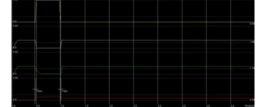
Figure 5: Timing (analog simulation) diagram for the CMOS Inverter
Technology (IJRASET)
Figure 7: Timing (analog simulation) Diagram for the STSCL Inverter The results are tabulated below based on the simulation verification of the both inverters.
TABLEI
PERFORMANCE COMPARISON OF A CMOS & STSCL INVERTER FOR DIFFERENT PARAMETER
Parameter CMOS
Inverter
STSCL Inverter Power
Consumption
0.103mw 23.102µw
Delay 0.979ns 0.979ns
Frequency 1.02GHz 1.02GHz
V. CONCLUSION
Sub-threshold region procedure is highly beneficial in order to reach a very low power-energy consumption specification. This sort of specs would be required for implementation of e. g. modern-day distributed sensor systems. Designers nowadays apply electric power reduction techniques in every degree of abstraction in order to achieve optimum level of power reduction. These kinds of reduction schemes must be used such that the value of maintaining the system performance is not sacrificed.
The area required for designing the STSC cellular library is notably higher than for CMOS. The area drawback is bearable when ultra-low energy usage per computation features high priority. Also, further minimization of the bias current is possible by resizing the differential NMOS network in the STSCL; this will lead to an additional reduction in conditions of energy consumption.
The major problems that can be faced with STSCL entrance for processes, is the occurrence of higher door leakage (can possibly be reduced by introducing devices with high-k dielectric), also reduction of bias current would require increasing the width of NMOS devices that can inadvertently improve the impact of the parasitic capacitance and might also raise the dynamic power intake. Thus, device sizing should be done properly, before heading for circuit implementation with STSCL standard cells.
Latest articles and papers show that current CMOS process or CMOS standard skin cells can be tailored and modified to run at sub-threshold region of procedure. The problem with such modifications, however, has long been the inconsistency in maintaining the CMOS gates to perform under sub threshold region of operation.
The reason being that basic CMOS technology is scaled and fabricated to operate under normal threshold condition. Different problems include process details, like sub threshold mountain factor, deeply impact CMOS logic procedure at sub-threshold region. To mitigate this problem, processes are needed to have better incline factor.
The impact of the several conditions mentioned above can be reduced, which in turn will permit the CMOS gates to perform at sub-threshold region really steady manner, but the cost increases. Transition from basic bulk CMOS technology to SOI technology, use of double gate CMOS, varying threshold voltage sub-threshold CMOS, etc. are a few examples where device level modification have been done in attempt of using CMOS to run at sub-threshold region for low voltage-low power digital app. All these device level modification will however in the end raise the architecture cost considerably and may switch out to be not that affordable.
REFERENCES
[1] Tajalli, E. J. Brauer, Y. Leblebici and E. Vittoz (2008), Sub-threshold Source-Coupled Logic Circuits for Ultra-Low-Power Applications, in IEEE JOURNALS of Solid-State Circuits, VOLUME: 43,Issue: 7, page(s): 1699-1710.
Technology (IJRASET)
design, in IEEE International Symposium of Circuits and Systems, ISCAS 2009, page(s): 2553-2556.[3] M. Alioto, University of California, Berkeley (U.S.A.), Sub-threshold VLSI circuits for ultra-low power/minimum-energy applications: from basics to advanced design strategies, Presented at Dipartimento di Ingegneria dell'Informazione, Universita di Siena – Italy.
[4] M. Azaga and M. Othman (2008), Source Couple Logic (SCL): Theory and Physical Design, in American Journal of Engineering and Applied Sciences 1 (1), page(s): 24-32.
[5] K.M. Cao, W.C. Lee, W. Liu, X. Jin, P. Su, S.K.H Fung (2000), BSIM4 gate leakage model including source-drain partition, in Electron Device Meeting, 2000, IEDM Technical Digest, page(s): 815-818.
[6] C. Enz, F. Krummenacher, E. Vittoz, Charged based MOS transistor Modeling: The EKV Model for Low-Power and RF-IC Design. New York: Wiley, 2006.
AUTHORSBIOGRAPHIES
Mr.B.V.Ramana has pursued his B.Tech from St.Johns College of Engg.& Tech, Yemmiganur and M.Tech from Sree Vidyanikethan Engineering College,Tirupathi. Presently he is working as Asst.Prof in Dept of ECE in Brindavan Institute of Technology & sciences, Kurnool. He has published 4 International Journals . His research areas of interest are Electronic circuit analysis & design, VLSI, Linear integrated circuit design, fault detection and testing of digital circuits ,Fault model analysis.
Mr.S.MD.Imran Ali has pursued his B.Tech from SAFA College of Engg.& Tech, Kurnool and M. Tech from KTMC , Kondair. Presently he is working as Asst.Prof in Dept of ECE in Brindavan Institute of Technology & sciences, Kurnool. He has published 5 International Journals .His research areas of interest are VLSI for signal & Image processing, Wireless communications, Antenna design, Analog & Digital communications, Digital integrated circuit design.
Mr P. Nagashyam of E.C.E department is pursuing his B.Tech in Brindavan Institute of Technology and science, Kurnool. His area of interest is VLSI.
Mr Y. Sandeep of E.C.E department is pursuing his B.Tech in Brindavan Institute of Technology and science, Kurnool. His area of interest is VLSI.