Investigation on the micro structural and surface
morphological properties of SILAR grown CdO
thin films by altering dipping cycle
M. Karunakaran1, M. Rajini2, S.Maheswari3, K.Kasirajan4, S.Dinesraj5 1,2,4,5
Department of Physics, Alagappa Government Arts College, Karaikudi – 630 003, India.
3
Department of Physics, Caussanel College of Arts and Science, Muthupettai - 623 523, India.
Abstract: Cadmium oxide (CdO) thin films were prepared by successive ionic layer adsorption and reaction (SILAR) method by altering dipping cycle. The prepared films were annealed at 2500C for 2 h. The prepared films were characterized by X-ray diffraction (XRD), optical spectroscopy and scanning electron microscopy (SEM) measurement. The XRD analysis reveals that the films were polycrystalline with cubic structure. Both crystallinity and the grain size were found to increase with increasing dipping. SEM analysis shows the porous nature of the surface with spherical nano clusters. Energy dispersive spectroscopic analysis (EDX) confirmed the presence of Cd and O elements.
Keywords: CdO, SILAR, X-ray diffraction, Crystallite size, SEM and FWHM.
I. INTRODUCTION
Transparent conducting oxides (TCOs) are potential candidates for energy efficient devices like solar cells, light emitting diodes, photo detectors because of their high transparency in the visible region and high electrical conductivity at room temperature [1]. Various oxides such as SnO2, In2O3, ITO, FTO, and CdO are used as transparent electrodes in solar cells and other optoelectronic
devices [2]. Cadmium oxide (CdO) is an II-VI compound n-type degenerate semiconductor with a simple cubic structure having a direct band gap of 2.3 eV [3]. Deposition techniques such as sputtering [4], metal-organic chemical vapor deposition (MOCVD) [6], pulsed laser deposition (PLD) [5], chemical vapor deposition (CVD) [7], spray pyrolysis [9], sol-gel technique [8], chemical bath deposition (CBD) [10] and successive ionic layer adsorption and reaction (SILAR) [11] technique have already been employed to prepare CdO thin films. Among these deposition techniques, SILAR has many advantages such as low cost, simplicity and reproducibility. Moreover anion and cation precursor in different baths offers good control over the deposition parameters such as pH, deposition temperature and time, etc [12]. The only disadvantage of this technique is the formation of hydroxide phase while oxide growth and slow growth rate. In this work, CdO thin films were prepared by SILAR method and the influence of dipping cycle on the structural, optical and transport properties of the CdO thin films are discussed in detail.
II. EXPERIMENTAL PROCEDURE
CdO thin films were prepared using a modified SILAR technique involving double dip. CdO thin films were grown using a two-step modified SILAR using a solution comprising 0.1 M cadmium acetate [Cd(CH3COO)2.2H2O) ( 99% e-Merck), 0.2 ammonium
hydroxide with a pH value of 70.2 deposited at bath temperature of 90 C under optimized condition. The complexing agent ammonium hydroxide was used to stabilize the crystallite size [13-14]. In normal SILAR four beakers were used. Anionic and cationic precursor solutions are taken in separate beakers. But in a modified SILAR all the precursor solutions are taken in a single beaker [15]. Before deposition, the glass substrates were cleaned in hot chromic acid followed by cleaning with an alkali and acetone. The well-cleaned substrates were immersed in the chemical bath for a known standardized time followed by immersion in hot water for the same time for hydrogenation. The process of solution dip (step 1) followed by hot water dipping (vary step 2) is repeated for known number of times such as 10, 15 and 20 cycle. The cleaned substrate was alternatively dipped for a predetermined period in ammonium cadmium bath and water bath kept at room temperature and near boiling point, respectively. The thickness of the coated films was measured using the surf test SJ – 301 stylus type surface roughness and thickness measuring instrument. X-ray diffraction analyses were obtained using the model X‟pert PRO (Analytical) X-ray powder diffractometer with Ni filtered CuKα
Spectrophotometer. The CdO thin film formed was confirmed by XRD (Rigaku Ultima III) analysis and the micro structural analyses of the samples were performed using SEM (JEOL Model JSM - 6390LV).
III. RESULTS AND DISCUSSION
A. Thickness Studies
Figure 1 shows film thickness variation as a function of solution concentration values. The film thickness was estimated by the weight gain method using the formula [16].
t = m / A --- (1)
[image:3.612.184.426.247.442.2]where ‘t’ is the thickness of the film, ‘m’ is the weight gain, ‘A’ is the area of the coated film and ‘’ is the density of the film. The film thickness increased with increase of dipping cycle. The film thickness was estimated to be approximately 610 nm, 635 nm and 680 nm for dipping cycle of 10, 20 and 30 respectively.
Figure 1. Film thickness variation of CdO thin films prepared at various dipping cycle.
B. XRD Studies
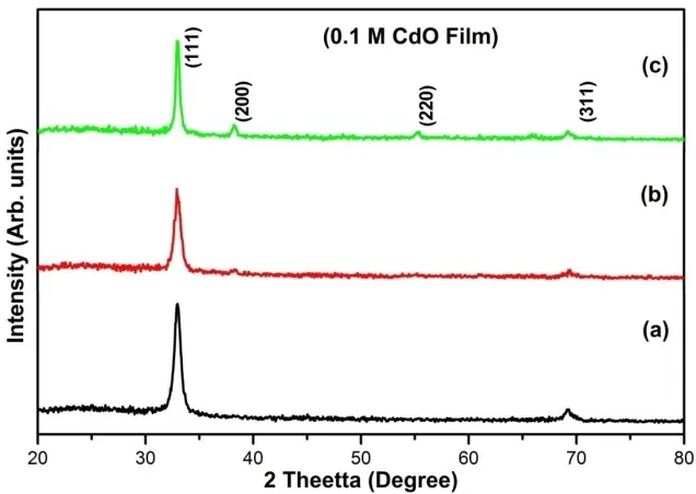
Figure 1 (a - c) shows the XRD pattern of the CdO thin films deposited using different dipping cycles. All the diffraction peaks of XRD pattern could be indexed to cubic crystal structure of CdO, which is in good agreement with the standard data for CdO (JCPDS data file no. 78-0653). This is in accordance with the reports on CdO thin films prepared by SILAR method. The grown CdO have exhibited strong orientation along (1 1 1) plane and also it has shown reflections along (2 0 0), (2 2 2) and (311) planes too. The intensity of the diffraction peak was also found to decrease with increasing dipping cycle and get sharper with decreasing full width half maximum (FWHM). This can be attributed to the improvement in crystallinity of CdO thin films. No other peaks appear.
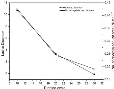
The structural parameters of CdO thin films are given in Table 1. The crystallite size is calculated using Debye - Scherrer’s formula [17-18]
D = k / cos --- (1)
Where k is the shaping factor which takes value from 0.89 to 0.94, ‘’ is the wavelength of the Cu-k line, ‘’ is the full width at
half maxima (FWHM) in radians and ‘’ is the Bragg’s angle.
Dislocation density (δ) for (111) plane is evaluated using the relation
δ = 1/D2 --- (2)
The strain (ε) is calculated from the following relation
The stacking fault probability (α) with peak shift Δ(2θ) was calculated by
tan
2
3
45
2
2
--- (4)The Lattice distortion (L.D) is calculated from using the formula
L.D = / 4 tan --- (5) The Number of crystallites per unit area is calculated from the following relation
[image:4.612.148.466.241.467.2]Nc = t / D3 --- (6)
Figure 2: CdO thin films of 0.1 M at (a) 10 dip (b) 20 dip (c) 30 dip
No. of Dipping
Crystallite size (D) nm
Strain
(ε) x 10-3
Dislocation density
δ x 1014
lines/m2 Stacking fault probability (α) Lattice Distortion (L.D)
No. of Crystals per unit area
(N) x 1016
10 16.19 2.13 38.13 1.29 10.95 0.42
20 27.02 1.28 13.69 2.16 3.09 0.25
30 40.40 0.85 6.12 3.54 0.78 0.17
Table 1. Microstructural properties of various dipping cycle prepared CdO thin films
[image:4.612.73.538.496.674.2]Figure 3: Variations of crystallite size and strain
[image:5.612.188.418.509.689.2]Figure 4: Variations of dislocation density and stacking fault probability
C. Morphological studies
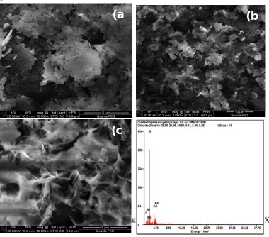
Figure 6 (a-c) shows the surface morphology of CdO thin films prepared at various dipping cycle such as 10, 20 and 30. SEM micrograph reveals the presence of uniformly sized spheroidal nanoclusters distributed over the surface. Obviously the tiny nanoclusters get agglomerated with each other while increasing the annealing temperature leads to the forming of bigger grains. The surface of the film is found to be heterogeneous, having porous surface with small pinholes. When the dipping increases, the pinholes over the surface get disappeared. The film prepared at 30 dipping cycle is found to have bigger grains with nanopores on the surface. The obtained spherical morphology with nanopores on the surface may deliver better performance for dye sensitized solar cells and gas sensor devices.
Fig 6 (a-c): SEM micrograph of CdO thin films (a) 10 dip (b) 20 dip (c) 30 dip (d) EDX
D. Elemental Analysis
Elemental analysis of CdO thin films was carried out by EDX. Figure 6 (d) represents the EDX spectrum of CdO thin film prepared at 30 dipping cycle. Analysis shows the presence of only Cd and O elements and Si peak which corresponds to the glass substrate. EDX analysis confirms the presence of Cd and O elements.
IV. CONCLUSION
CdO thin films were fabricated on glass substrate using modified SILAR method by altering dipping cycle. XRD studies show that all the films are polycrystalline in nature with cubic structure having preferential orientation along (2 0 0) plane. It is observed from the SEM images and XRD patterns that the grain sizes of the structures were increased with dipping cycle. The EDX analysis conform the presence of Cd and O elements in the prepared thin films.
REFERENCES
[1] Saha, S. Das, K.K. Chattopadhyay, Sol. Energy Mater. Sol. Cells 91 (2007) 1692-1697.
[2] K. Gurumurugan, D. Mangalaraj, S.K. Narayandass, C. Balsubramanian, Phys. Stat. Sol. 143 (1994) 85-91.
(a
)
(c
)
(b
[image:6.612.101.481.189.523.2][4] K. Gurumurugan, D. Mangalaraj, Sa.K. Narayanadass, J. Cryst. Growth 147 (1995) 355-360. [5] Z. Zhao, D.L. Morel, C.S. Ferekides, Thin Solid Films 413 (2002) 203-211.
[6] R.K. Gupta, K. Ghosh, R. Patel, S.R. Mishra, P.K. Kahol, Mater.Lett. 62 (2008) 4103-4105. [7] X. Liu, C. Li, S. Han, J. Han, C. Zhou, Appl. Phys. Lett. 82 (2003) 1950-1952.
[8] R. Ferro, J.A. Rodriguez, Thin Solid Films 347 (1999) 295-298.
[9] R. Maity, K.K. Chattopadhyay, Sol. Energy Mater. Sol. Cells 90 (1995) 597-606. [10] A.J. Varkey, A.F. Fort, Thin Solid Films 239 (1994) 211-213.
[11] M.A. Yilidirim, A. Ates, Sens. Actuators A 155 (2009) 272-277.
[12] B. Gokul, P. Matheswaran, R. Sathyamoorthy J. Mater. Sci. Technol., 2013, 29(1), 17-21.
[13] M. Karunakaran, R. Chandramohan, S. Balamurali, S. Gomathi, K. Kabila, T. Mahalingam, Int. J. Thin Film. Sci. Tec. 3, No. 2, (2014) 61-65. [14] M. Mahaboob Beevia , M.Anusuyab, V.Saravananc, Int J Chem Eng Appl. (2010) 1 (2), 151-154.
[15] M. Karunakaran, K. Rubanancy, M. Rajini, G. Kavitha and R. Chandramohan, 02, No.01, (2016), 84-89.
[16] S. Valanarasu, V. Dhanasekaran, M. Karunakaran, R. Chandramohan, T. Mahalingam J. Nanosci. Nanotechnol.13, (2013) 1–6. [17] B.D. Cullity, Elements of X-Ray Diffraction, Addison-Wesley Publications Company Inc, Reading, Massachusetts, 1956.
[18] Valanarasu S, Dhanasekaran V, Karunakaran M, Chandramohan R, Mahalingam T. Role of solution pH on the microstructural properties of spin coated cobalt oxide thin films. J. Nanosci. Nanotechnol. 2013; 13:1–6.
[19] Dhanasekaran V, Mahalingam T. Surface modifications and optical variations of (− 111) lattice oriented CuO nanofilms for solar energy applications. Mater. Res. Bull. (2013), 48(9), 3585–3593.
[20] Hussain S, Sathiyaraj K, Joseph Prince J. Tunability of ZnO optical band on varying Zn2+ concentration. International Journal for Research in Applied Science
& Engineering Technology. (2014), 2(10), 100-105.