5
III
March 2017
Technology (IJRASET)
Design and Implementation of Dc-Dc Buck Boost
Converter by using 8051 Microcontroller
Shital J Sawant1, Snehal H Patil2, Savita M Patil3 , Pranita P Patil4 , Varsha S Nikam5 , Renu C Lohana6 1,2,3,4,5,6
Electrical Engineering Department, NMCOE, Shivaji University, India
Abstract: This paper presents design and implementation of DC-DC Buck Boost converter by using 8051 microcontroller. The switched mode dc-dc converters are most widely used electronic circuits for its high conversion efficiency and flexible output voltage. These converters are designed to regulate the output voltage against the changes in the input voltage. Many existing and developing electrical and electronic technologies require the voltage of different levels that are supplied from an available source voltage such as a battery. DC-DC Buck Boost converters are devices designed especially for maintaining constant DC output voltage, if the supply voltage is variable. The demand for compact power supplies has grown significantly. Power supplies with low cost, high efficiency and smaller size are required. To control the output voltage of the converter, the controller is designed to change the duty cycle of the converter. In this converter, IGBT switch is digitally controlled by 8051 microcontroller. The circuit is simulated in MATLAB SIMULINK and then the results are verified with hardware implementation. This paper focuses on the hardware design and implementation of DC-DC Buck Boost converter. This converter is used as a voltage regulating device and mainly used where the load is very sensitive.
Keywords: DC-DC Buck Boost converter, Duty cycle, 8051 microcontroller, IGBT’s.
I. INTRODUCTION
DC – DC Buck Boost converters are electronic devices which are used whenever we want to change DC electrical power efficiently from one voltage level to another. High frequency switching converters are used as interfaces between DC systems of different voltage levels. These converters are known as high-frequency DC - DC converters. They are used in the power supplies and other electronic equipment. This switching converter can also be used as an interface between DC and AC systems. High voltage DC is required for several applications in the field of electrical engineering and applied physics such as X-ray units, electron microscopes which require high DC voltages of the order of 100 kV or more. It is also used in electrostatic precipitator railway coaches, UPS system and drives application.
The converter is able to deliver output voltages both higher as well as lower than (or even equal to) the input voltage, so it is referred as a buck-boost power converter. In this topology, basically IGBT is used as switch operating at 30 kHz switching frequency and 8051 microcontroller is used for controlling the operation of converter. This controller adjusts the duty ratio and gives proper output. The input range of this DC to DC converter is 90 V-250 V & output range is 200 V, 5 A.
II. DC-DCBUCKBOOSTCONVERTERSYSTEM
The Buck-Boost or Inverting regulator takes a DC input voltage and produces a DC output voltage that is opposite in polarity to the input. The negative output voltage can be either larger or smaller in magnitude than the input voltage. The Inverting regulator is shown in Fig.1[2],[3].
Technology (IJRASET)
When the switch is ON, the input voltage is forced across the inductor, causing an increasing current flowing through it. During the ON time, the discharge of the output capacitor is the only source of load current. The charge lost from the output capacitor during the ON time should be replenished during the OFF time.
When the switch turns OFF, the decreasing current flows through the inductor causing the voltage at the diode end to swing negative. This action turns on the diode, allowing the current in the inductor to supply both the output capacitor and the load. As shown in Fig. 2, the load current is supplied by inductor when the switch is OFF(Boost mode) and by the output capacitor when the switch is ON(Buck mode). Waveforms of buck-boost converter is as shown in Fig.3.
Fig .3 Waveforms of buck-boost converter
III. HARDWAREDESIGNANDIMPLEMENTATION
A. Block Diagram
[image:3.612.198.432.406.540.2]The block diagram of Buck Boost Converter is as shown in Fig. 4. It consists of switching device, capacitor, inductor, SMPS, driver card, feedback circuit and microcontroller.
Fig.4 Block Diagram of Buck Boost Converter
Basically, the input voltage is varied from 90 to 250V. Switching devices used may be IGBT or MOSFET, but here 3 IGBT’s are used for switching purpose. Capacitor is used to store the energy in the form of electric field, while inductor is used to store the energy in the form of magnetic field. Feedback circuit consist of ADC (Analog to Digital Controller) & it compare the input voltage & output voltage and gives the digital signal to the microcontroller. Microcontroller is a decision making device. It takes difference between the input and output voltages and decides whether to buck or boost the voltage so as to get the constant output voltage. The gate pulses are provided to the IGBT’s. SMPS (Switched Mode Power Supply) is used to provide 5V DC supply to the microcontroller & 12V DC supply to the Driver card. Driver card is used for driving the IGBT’s. The voltage across the load is maintained constant by varying the duty cycle D[2],[3].
Technology (IJRASET)
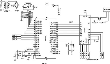
Ton is ON time(conducting period) of IGBT, [image:4.612.86.532.107.368.2]Toff if OFF time(non-conducting period) of IGBT as shown in Fig. 3.
Fig.5 Connections of microcontroller with ADC and IGBT
Initially, 230V AC supply is step down to 12V AC by using step down transformer and then it is rectified to 12V DC supply. This 12V DC supply is then fed to IGBT and driver circuit and to the microcontroller unit. IGBT’s are connected to port 1 to the pin
no.1.0, 1.1, 1.2. Port 0 is always grounded through 1 kΩ resistors. LCD display is connected to port 3. Here 0808 Analog to Digital
converter is used. It is connected to port 2. Quartz crystal oscillator having frequency 11.059MHz is used. The circuit connections for microcontroller are as shown in Fig. 5.
Fig. 6 IGBT & Driver Circuit
[image:4.612.156.466.472.655.2]Technology (IJRASET)
IV. COMPONENTDESCRIPTION
A. Microcontroller 89C51
The AT89C51 is a high performance, low-power, CMOS 8-bit microcontroller. It has 128 bytes of RAM and 4K bytes of flash programmable and erasable read only memory(EPROM). This device is manufactured using Atmel’s high-density non-volatile memory technology. The Atmel AT89C51 is a powerful microcomputer which provides a highly flexible and cost-effective solution to many embedded control applications.
The AT89C51 microcontroller is designed with static logic for operation down to zero frequency. It supports two software selectable power saving modes. 8051 microcontroller is a small computer on a single integrated circuit. The microcontroller is a decision making device which decides on and off operation of the converter.
1) Features of 89C51:
a) Compatible with MCS-51TM Products.
b) 4K Bytes of In-system Programmable Flash Memory Endurance
c) 1,000 Write / Erase Cycles.
d) Fully Static Operation: 0 Hz to 24 MHz
e) Three-level Program Memory Lock
f) 128 x 8-bit Internal RAM
g) 32 Programmable I / O Lines.
h) Two 16-bit Timer / Counters
i) Six Interrupt Sources
j) Programmable Serial Channel
k) Low-power Idle and Power-down Modes
B. Three Terminal Voltage Regulator
A voltage regulator is a three terminal regulator in which the output voltage is set at some predetermined value. This regulator does not require an external feedback connection. Hence, only three terminals are required for device of such types, input (Vin), output (Vo) and a ground terminal. The voltage regulator operates at a preset output voltage and the internal current limiting resistor is also provided to the device. The main advantages of this regulator are the simplicity of connections to the external circuit and the minimum number of external components required. The voltage regulator is used for providing the regulated voltage to the microcontroller unit.
1) Features:
a) Internal thermal overload protection.
b) No external components required.
c) Output transistor safe area protection.
d) Internal short circuit current limit.
e) Circularity allows start up even if output is pulled to negative voltage.
2) Absolute Maximum Ratings:
a) Input voltage = 35 V
b) Internal power dissipation = Internally limited.
c) Operating temperature range = 0° C to 70° C
d) Maximum junction temperature = + 125°C
e) Storage temperature range = - 65° C to 150°C
f) Lead temperature = + 230° C
C. Capacitors
Capacitors store electric charge. Capacitor is used to smooth varying DC supplies by acting as a reservoir of charge. It is also used in filter circuits because capacitors easily pass AC (alternating) signals but it blocks DC (constant) signals. Electrolytic capacitors
are used having rating of 1000 μF. Here, capacitor is used for stepping up (boosting) of the voltage.
Technology (IJRASET)
Diodes allow electricity to flow in only one direction. Here diodes are used for making bridge rectifier. Bridge rectifier consists of two parallel branches of diodes. Each branch consists of two diodes. Diodes are made up with semiconductor materials such as silicon, germanium and selenium. Diodes vary in both physical size and voltage capacity.
E. Light Emitting Diodes (LEDs)
LEDs emit light when an electric current passes through them. LED lamp is used as load.
They are available in different colors like red, orange, amber, yellow, green, blue and white. Blue and white LEDs are much more expensive than the other colours. The colour of an LED is determined by the semiconductor material and not by the coloring of the plastic body. LED lamp is used as a load.
F. Presets
These are miniature versions of the standard variable resistor. Presets are designed to be mounted directly on the circuit board and adjusted only when the circuit is built. For example, to set the sensitivity of a light sensitive circuit and frequency of an alarm tone. A small screwdriver is required to adjust presets.
Presets are much cheaper than standard variable resistors, hence they are sometimes used where a standard variable resistor would normally be used. Multi-turn presets are used where very precise adjustments are necessary to be made.
G. LCD display
This display consists of two internal byte resistors, one for the commands (RS=0) and second for character to be displayed (RS=1). It also consists of a user programmed RAM area that can be programmed to generate any desired character that can form using a dot matrix. Port 1 is used to furnish the command or data byte and ports 3.2 to 3.4 furnish register select and read/write levels. The display takes varying amounts of time to accomplish the function. LCD display is used to indicate the bucking and boosting operation of converter[4].
H. Optocoupler
The optocoupler is also called as optoisolator. Its main function is to prevent changing voltage on one side of circuit from damaging components on the other side of circuit. Here, 4N25 optocoupler is used. It consists of LED whose light energy is given to transistor. It is made up of light emitting device and light sensitive device wrapped up in one package. There is no direct connection between transistor and LED.
V. SYSTEMHARDWAREDESIGNING
System hardware designing is divided into 2 sections CPU Board
Input Board
A. CPU Board Designing
In this project, 89C51 micro-controller is used as CPU. 89C51 micro-controller requires some extra supporting hardware like + 5 volt power supply, POR as well as manual RESET, Clock generator and pull up resisters.
1) Power Supply:: For getting +5 volts supply, the + 12 volts supply from power supply output is taken and it is given to 7805 voltage regulator. The minimum input to 7805 is +7 V DC and maximum input is + 35 V DC. Here, + 12 V DC is used as an input to the 7805. Therefore, the output of the 7805 is constant regulated +5 Vdc.
2) POR and Manual RESET: When the power supply of the CPU board is switched ON, then micro-controller is RESET to start
the program execution from 0000H memory location. Therefore, POR (Power On Reset) is must. For this purpose, RC differentiator circuit is used. RC differentiator circuit provides logic high pulse to RESET pin of 89C51, when power supply is switched ON. Sometimes, manual RESET may be required. For this purpose, one push to ON tact switch is used. When this tact switch is pressed, then logic high signal is given to the RESET pin of the micro-controller 89C51.
3) Clock Generator: The maximum clock frequency of the micro-controller 89C51 is 24 MHz. Therefore, any frequency within 24
Technology (IJRASET)
4) External Pull Up Resistor: In micro-controller port 0 does not have internal pull up resistor, therefore external pull up resistor is used at port 0. At other ports, external pull up resistor is optional.
B. INPUT Board Designing
In INPUT board, operation mode is selected. The selection switches are used to select the following modes- PCB Etching Machine Start and PCB Etching Machine Stop. Again in input mode, limit switches are used. They are normally open. When direction is detected, then they will close. Logic 1 is for direction detection, otherwise logic 0 is gated[1].
VI. HARDWAREIMPLEMENTATIONOFDC-DCBUCKBOOSTCONVERTER
Fig. 6 Completely mounted DC-DC Buck Boost Converter
230V, 50Hz AC supply is given to the step-down transformer to reduce the voltage to 12V. After that, 12V supply is given to the bridge rectifier and to convert AC into DC. Then, DC is fed to microcontroller, IGBT and driver circuit. The microcontroller is programmed such that the LCD display indicates bucking or boosting operation of converter. Feedback circuit consist of ADC (Analog to Digital Controller) & it compares the input voltage with output voltage and gives the digital signal to the microcontroller. Microcontroller determines the ON and OFF periods and the corresponding PWM pulses are fed to the gate of IGBT.
VII. EXPERIMENTALRESULTS
The input voltage and the output voltage is measured using the multimeter, during the boost mode and buck mode. The hardware results are displayed in Table I below. It is observed that the converter increases voltage during boost mode and decreases voltage during buck mode. The results are quiet satisfactory to maintain constant voltage. Thus the results are verified by hardware implementation.
TABLE I
INPUT AND OUTPUT VOLTAGES FOR BOOST AND BUCK MODE
Operation Input Voltage Output Voltage
Boost Mode 90V 199V
Technology (IJRASET)
VIII. CONCLUSION
Thus, with variable input voltage, the load voltage is maintained constant by using DC-DC buck boost converter. This buck boost converter system is controlled by AT89C51 microcontroller. Hardware implementation is successfully carried out by interfacing microcontroller with ADC and PWM analysis. The high power quality buck boost converter is better solution for speed control of DC series motor and battery powered products.
IX. ACKNOWLEDGMENT
We are thankful to our guide Asst. Prof. Ms. Lohana R. C. of Nanasaheb Mahadik College of Engg (NMCOE), Peth affiliated to Shivaji University, Kolhapur for her co-operation, constant inspiration and support to implement this work.
REFERENCES
[1] Bhim Singh, Rahul Pandey, “Improved Power Quality Buck-Boost Converter fed LLC Resonant Converter for Induction Heater”, IEEE 6th International
Conference on Power Systems(ICPS), Electronic ISBN: 978-1-5090-0128-6, Print on Demand(PoD) ISBN: 978-1-5090-0129-3, Mar 2016. [2] K. B. Khanchandani and M. D. Singh, “Power Electronics”, 2nd Edition, Mc Graw Hill education (INDIA), ISBN-0-07-058389-7, 2015. [3] M. H. Rashid, “Power Electronics: Circuits, Devices and Applications”, 3rd Edition, Prentice Hall, 2003.
[4] Jaber Abu-Qahouq and Issa Batarseh, “Generalized Analysis of Soft-Switching DC-DC Converters”, IEEE 31st Power Electronics Specialists Conference
(PESC), Vol. 3, June 2000.