N A N O E X P R E S S
Open Access
Axially connected nanowire core-shell p-n
junctions: a composite structure for
high-efficiency solar cells
Sijia Wang, Xin Yan, Xia Zhang
*, Junshuai Li and Xiaomin Ren
Abstract
A composite nanostructure for high-efficiency solar cells that axially connects nanowire core-shell p-n junctions is proposed. By axially connecting the p-n junctions in one nanowire, the solar spectrum is separated and absorbed in the top and bottom cells with respect to the wavelength. The unique structure of nanowire p-n junctions enables substantial light absorption along the nanowire and efficient radial carrier separation and collection. A coupled three-dimensional optoelectronic simulation is used to evaluate the performance of the structure. With an excellent current matching, a promising efficiency of 19.9% can be achieved at a low filling ratio of 0.283 (the density of the nanowire array), which is much higher than the tandem axial p-n junctions.
Keywords:Solar energy; Nanophotonics and photonic crystals; Semiconductors
Pacs codes:88.40.H-; 88.40.jp; 81.07.Gf
Background
The development of high-efficiency photovoltaic (PV) systems has been a topic of intensive research recently. Most efficient solar-energy-harvesting devices are fabri-cated using compound III-V semiconductor materials in an advanced multi-junction structure [1-3]. However, the higher costs of III-V materials, increased complexity, and manufacturing price have been inhibiting the commercial application of multi-junction solar cells. A possible solu-tion of this problem is to adopt III-V semiconductor nano-wires (NWs) for solar cells.
NWs exhibit excellent properties for PV applications. It has been widely demonstrated that NWs with a well-defined geometrical structure can achieve higher light absorption than their thin-film counterparts with reduced material use, by combining intrinsic anti-reflection and enhanced light trapping [4-9]. In addition, the unique geometry of the NW enables the formation of advanced heterostructures, which can improve the performance of solar cells substantially. For example, benefiting from the highly effective lateral stress relaxation at the NW sidewall
[10,11], high-quality p-n junctions with different bandgaps can be stacked into a single NW, which dramatically expands the absorption spectrum. Another promising structure is the core-shell p-n junction, which enables substantial light absorption along the long axis of the NW and efficient radial carrier separation and collection [12,13]. Furthermore, the pure ‘axial’ or ‘radial’ tandem solar cell also has its limit. Because the photogeneration events happen most frequently at the center of NWs, the axial junction cannot intrinsically block the generated car-riers from reaching the surface and recombining like the radial junctions. Due to a similar reason, the radial tandem solar cell faces a challenge in efficient absorption for the shell junctions away from the core of NWs. Thus, it is not difficult to imagine that a composite structure which combines the advantages of the‘axial’and‘radial’ structures would provide much higher efficiency compared with homogeneous ones.
In this paper, we propose a novel NW composite nanostructure for high-efficiency solar cells. The structure consists of several core-shell p-n junctions with different III-V materials which are axially connected by the tunnel diode in a NW. The stacked subcells with different bandgaps can exploit the solar spectrum very effectively. The core-shell p-n junction in each subcell provides an * Correspondence:[email protected]
State Key Laboratory of Information Photonics and Optical Communications, Beijing University of Posts and Telecommunications, No. 10. Xitucheng Road, Beijing 100876, China
efficient collection of photogenerated carriers, which leads to a high photocurrent. A coupled three-dimensional (3-D) optoelectronic simulation is used to explore the photo-voltaic efficiency of the structure. Finite-difference time-domain (FDTD) method is employed to investigate the light absorption characters and light trapping effects of the NW array. After the optimization, a high conversion efficiency of 19.9% is obtained at a low filling ratio of 0.283 (the filling ratio is defined as the area ratio between the total top surface of the NW arrays and the substrate), which is much higher than that of the tandem axial p-n junction counterpart.
Methods
Device design
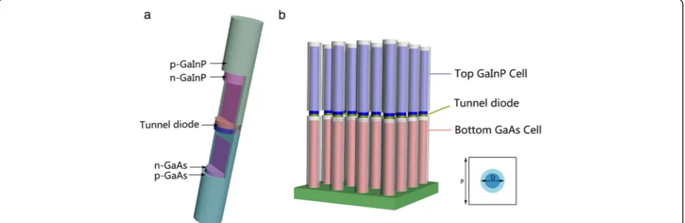
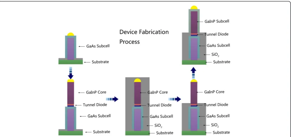
The schematic of the structure is shown in Figure 1a. Each subcell consists of an n-type NW core encapsu-lated in a p-type NW shell, which can be achieved by controlling the growth temperature to realize the switch between the core shell and axial growth [14-17]. The growth of GaAs nanowire arrays can be achieved using gold seed particles in arrays which can be arranged by a nanoimprint lithography. The core diameter and the period of arrays can be controlled by tuning the sizes and array pitches of the Au seeds [18]. The detailed fab-rication process is shown in Figure 2. Different subcells can be connected by using a p++-n++tunnel diode which bridges the p-shell of lower subcell and n-core of the subcell above. The high-performance single nanowire tunnel diodes have been reported recently [19]. Thus, the composite structure is practically achievable via trad-itional vapor-liquid-solid (VLS) growth method [20,21]. In the simulation, the top cell is composed of Ga0.5In0.5P
with a bandgap of 1.8 eV, while GaAs with a bandgap of 1.42 eV is chosen for the bottom cell, for the purpose of absorbing the incident sunlight sufficiently with a practical
lattice-matching. For each subcell, a core-shell p-n junc-tion configurajunc-tion is employed with a n-type core NW and a p-type shell NW, which are uniformly doped to 1 × 10¹⁷ and 3 × 1018 cm−3, respectively, while the doping concentration of the n-type GaAs substrate is 1 × 1017 cm−3. The lengthL of each subcell is fixed to 2 um, which is comparable to the film thickness in III-V solar cells. As shown in Figure 1b, the tandem NWs are arranged in a square array, where the D/P ratio determined by the period of the square lattice (P) and the diameter of NWs (D) is set to 0.5. For small D/P ratio, the incident light cannot be coupled into the NW and absorbed efficiently, resulting in a decrease in the conversion efficiency. However, higher D/P ratio means more consumption of Ga and In element, which are not found abundant in the earth crust and thus very expensive. Meanwhile, the efficiency does not always increase with increasing D/P ratio and has a upper limit. Thus, we select a relative lowD/Pratio of 0.5 to achieve a good balance between the light absorp-tion and material consumpabsorp-tion [22]. The tunnel diode is assumed to be ideal (i.e., resistive or optical absorption losses are neglected) [23]. To isolate the GaInP shell from the tunnel diode in electrics, a transparent dielectric ma-terial, e.g., SiO2is placed around the tunnel diode.
Simulation method
[image:2.595.58.540.535.692.2]Optical properties of the structure are investigated using Sentaurus Electromagnetic Wave (EMW) Solver module package. The axially connected NW core-shell p-n junc-tions are theoretically analyzed by using 3-D FDTD simu-lations [24-26]. The minimum cell size of the FDTD mesh is set to 5 nm, and the number of nodes per wavelength is 20 in all directions. By placing periodic boundary condi-tions, the simulations can be carried out in a unit cell to model the periodic array structure. A perfect matching
layer (PML) is used under the GaAs substrate to assume semi-infinite substrates for simplified computation. The wavelength-dependent complex refractive index used in the simulations is obtained from the SOPRA N&K Data-base [27]. Normally, incident light is defined with power intensity and wavelength values from a discretized AM 1.5G solar spectrum. The AM 1.5G spectrum is divided into 62 discrete wavelength intervals, from 290 to 900 nm. The corresponding unpolarized feature of sunlight is modeled by superimposing the transverse electric (TE) and transverse magnetic (TM) mode contributions. To obtain the total optical generation under AM 1.5G illumi-nations, the power-weighted photogeneration rates of a single wavelength are superimposed from the FDTD simulation results [28,29]. The optical generation rate Gph
is obtained from the Poynting vector S:
Gph¼
∇ →
⋅S→
2ℏω ¼
ε″E→2
2ℏ ð1Þ
whereE is the electric field intensity at each grid point,
ω is the angular frequency of the incident light,ℏ is the reduced Planck's constant, and ε'' is the imaginary part of the permittivity.
For the electrical modeling, the 3-D optical generation profiles are incorporated into the finite-element mesh of the NWs in the electrical tool [29]. The device electrical simulation takes the doping-dependent mobility (GaAs only) and bandgap narrowing, radiative, Auger and Shockley-Reed-Hall (SRH) recombinations into con-sideration. The material parameters critical for device
simulations are mostly obtained from the Levinshtein model [30], which is shown in Table 1. The Arora model [29,31] is adopted in the calculation of the doping-dependent mobility, which reads:
μdop¼μminþ
μd
1þðN=N0ÞA
ð2Þ
where A is 0.6273 (0.8057) and N0 is 7.345 × 10¹⁶ (5.136 × 10¹⁷)/cm3for the electrons (holes). The current-voltage relationship which is calculated by:
J¼Jsc−J0 expV=Vc−1
ð3Þ
whereJ is the current density of the solar cell, Jsc is the photocurrent density,J0is the reverse saturation current density, and V is the voltage between the terminals of the cell. Vc is the thermal voltage, which can be given by:
Vc¼KBTc
q ð4Þ
[image:3.595.60.539.88.314.2]in which KB is the Boltzmann constant, Tc is the cell temperature, and q is the elementary charge. For the tandem structure of dual-junction cell, the short-circuit current is determined by the smallest one of the subcell, and the open-circuit voltage is presented as the sum of subcells' voltages. To obtain high conversion efficiency, a current matching between the top GaInP cell and the bottom GaAs cell is needed. It has been reported that the light absorption and reflection of NWs is highly
Figure 2The fabrication process of the proposed structure.After growing the tunnel diode and GaInP core nanowire, we mask the device by SiO2, and then the SiO2mask is etched to the position which is a little higher than where the tunnel diode lies, in order to isolate GaInP shell
sensitive to the NW diameter due to the diameter dependent dispersion properties in the NWs [32,33]. To determine the ideal structure for current matching, a wide range of diameters (150 ~ 400 nm) are considered.
[image:4.595.57.538.100.183.2]Results and discussion
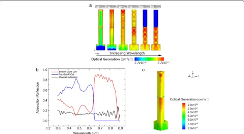
Figure 3a displays vertical cross sections of optical gen-erations through the center of NWs with increasing wavelengths under 1 kW/m2illuminations. The result shows a clear separation of absorption spectrum. At
λ= 350 nm, photocarriers are mainly generated at the surface of the NWs, showing a fairly short absorption length due to the high absorption capacity of GaInP and GaAs. At slightly longer wavelengths such as 450 nm, we can see that the majority of light is absorbed at the top GaInP cell. As wavelength increases, the optical
generation becomes more spread through the NWs, while more and more light can be transmitted and absorbed by the bottom cell.
Figure 3b shows the absorption and reflection spectra of the simulated GaInP/GaAs solar cell at a fixed D/P ratio of 0.5. As can be seen in the spectra, different cells absorb light in different ranges, which shows a promis-ing ability to achieve an excellent current matchpromis-ing when the subcells are axially connected. It can be seen that the total reflectance is lower than 0.2 from 290 to 900 nm due to the low effective refractive index, show-ing a good anti-reflection capacity. And the total ab-sorptance for two junctions is higher than 80% which demonstrates the incident sunlight can be coupled into the nanowires efficiently with the excellent light trapping and anti-reflection.
Table 1 Key material parametersa
Parameters Values
Minimum mobility (cm2/V · s) 2.136 × 10³(21.48) 2.3 × 10³(1.12 × 10²)
SRH lifetime (ns) 1 (1) 10 (10)
Effective density of states (/cm3) 4.42 × 10¹⁷(8.47 × 10¹⁷) 1.17 × 10¹⁸(1.98 × 10¹⁹)
Auger coefficient (cm6/s) 1.9 × 10⁻³¹(1.2 × 10⁻³¹) 3.0 × 10⁻³⁰
Surface recombination velocity (cm/s) 107(107) 107(107)
a
[image:4.595.58.538.429.692.2]Unless mentioned specifically, all simulations in this work use the parameters in this table by default. The numbers in the front and in the parentheses are for the electrons and holes, respectively.
Figure 3Optical generation and total photogeneration profiles, absorbance of the subcells and overall reflectance. (a)Optical generation profiles calculated by FDTD for wavelengths at 350, 450, 550, 650, 750, and 850 nm under 1 kW/m2.(b)The absorptance of the
Benefiting from the good light trapping and anti-reflection schemes, the incident sunlight can be effi-ciently absorbed by NWs at a low filling ratio. The total optical generation profiles in a quarter of the structure are shown in Figure 3c. Most of the photocarriers are generated in the first hundreds of nanometers of the NWs with a filling ratio of 0.196, implying an excellent optical absorption capacity in NWs.
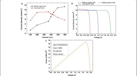
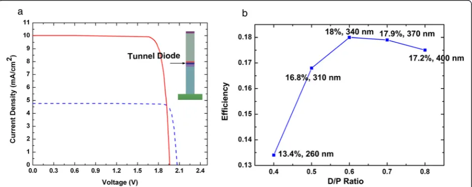
By tuning the diameters of NWs, the current matching is achieved at the NW diameter of 310 nm finally. The current densities for each subcell as a function of the NW diameter (150 to 400 nm) are shown in Figure 4a. For smaller diameters, the photocurrents are limited by the low light-trapping ability. Then, the photocurrents increase with the increasing diameter at first. When the diameter is further increased, the photocurrent in the top GaInP cell decreases due to the reduced absorption of dominant modes. More light not absorbed by the top cell is coupled into the bottom cell, resulting in a rapid increase of current density. And the simulated current-voltage characteristics of the subcells are shown in Figure 4b with an excellent current matching. The total J-V characteristic yields a short-circuit current (Jsc) of
10.02 mA/cm2and an open-circuit voltage (Voc) of 1.96 V.
The power conversion efficiency (PCE) and the filling fac-tor (FF) of the proposed structure, which can be obtained from the power-voltage characteristics shown in Figure 4c,
are 16.8% and 0.855, respectively. In comparison, GaAs (GaInP) radial single junction devices with a length of 2 um under the same condition yields 13%, 21.3 mA/cm2, 0.811 V (12.8%, 12.3 mA/cm2, 1.26 V). In consideration that the material consumption is just 0.2 of the thin-film solar cells, the performance is comparable to the state-of-the-art GaInP/GaAs dual-junction solar cells (27%) under the illumination of 1 sun (AM 1.5G) [34]. A sin-gle GaAs-based solar cell has been recently reported to have a short-circuit current density over 160 mA/cm2 [35,36]. There is a main difference in the calculation of short-circuit current density (Jsc) and efficiency between
the single nanowire and nanowire arrays, that is, the area used to divide the short-circuit current (Isc) is the
top surface area of nanowire in the single nanowire case, instead of the substrate area in the case of nanowire arrays. Therefore, the Jsc of nanowire array is always
lower than the single nanowire device. The highest ever recorded efficiency of nanowire arrays is 13.8%, which is reported by Wallentin's work [18]. Fine adjustments of bandgap combination and more subcells with a lower bandgap such as Ge are believed to enhance the per-formance even further.
Comparison with axial p-n junctions
[image:5.595.56.540.423.693.2]To assess the advantage of core-shell p-n junction NW, the PV performance of the tandem axial p-n junctions
on n-type GaAs substrate with the same volume and doping concentration is also simulated. For a relatively low loss of light when transmitted in the n-doped region, the NW axial p-n junction is employed with a short n-type region (100 nm) and a long p-type region (1,900 nm), at a fixedD/Pratio of 0.5. A coupled optoelectronic simulation and current matching which is same as the abovemen-tioned are carried out to obtain the J-Vcharacteristics. Figure 5a shows the comparison of J-V characteristics between the axial and core-shell p-n junctions. As can be seen from the figure, the axial one yields a higherVoc
(2.07 V) but a much lowerJsc(4.77 mA/cm2), which
re-sults in lower efficiency (8.87%). The higherVocmay be
explained by the larger depletion region in the axial p-n junctions. The width of the depletion region mainly depends on the material and doping concentration. However, the p-doped region (shell) in the radial p-n junctions is very thin, which may cause smaller deple-tion region. And the much lowerJsccan be explained by
the large absorption area along the axial direction and efficient carrier collection in core-shell p-n junctions. For the majority of wavelengths absorbed in GaInP/ GaAs, light is transmitted through the NW as shown in Figure 3a, which cannot be absorbed sufficiently by the axial p-n junction due to the small area and fixed pos-ition of depletion region. Subsequently, the short collec-tion length in NW core-shell p-n junccollec-tions promote the efficient collection of the photocarriers, which provides a further higher current density.
Device optimization
As mentioned above, the performance of the structure with a fixed D/P ratio of 0.5 is not optimal for the
maximum efficiency. And the nanowire density has an important impact on the device performance [37]. In this section, the PV performance with differentD/Pratio is simulated as shown in Figure 5b. With increasingD/P ratio, the conversion efficiency increases first and then decreases, obtaining a highest efficiency of 18% at aD/P ratio of 0.6 and NW diameter of 340 nm. The Jsc is
11.1 mA/cm2and Vocis 1.94 V. This phenomenon can
be understood by the increased light reflection at the top surface of NWA. The effective refractive index of the NW arrays increases asD/Pratio increases, resulting in the decline of anti-reflection capacity. Furthermore, in consideration to the fact that GaAs and Ga0.5In0.5P is
lattice matched, high-quality nanowires with little defect are expected to be achieved. Thus, a largerτSRHof 10 ns
can be adopted and a further improved efficiency of 19.9% (Jsc= 11.5 mA/cm2andVoc= 2.04 V) can be obtained
with aD/Pratio of 0.6 after the current matching. There is still some room for improvement in the optimization of the device, and a more precise and optimal estimate of effi-ciency will be presented in our future work.
Conclusions
[image:6.595.59.539.504.694.2]In summary, a novel NW structure for solar cells that axially connects core-shell p-n junctions with different bandgaps is proposed in this paper. A coupled three-dimensional optoelectronic simulation is used to evaluate the performance of the proposed structure. FDTD method is employed in the optical simulation. An excellent current matching of subcells is achieved by adjusting the diameter of the NWs. The simulation results reveal a high conver-sion efficiency of 16.8% at a low filling ratio of 0.196. Comparison with tandem axial p-n junctions is made,
indicating that core-shell p-n junctions have a much higher photocurrent under the same conditions. Some device optimization is made and a maximum efficiency of 19.9% is achieved by tuning theD/Pratio of the NW arrays and τSRH. By adopting optimized bandgaps or
more junctions, the performance of the proposed struc-ture is expected to be further improved.
Abbreviations
EMW:electromagnetic wave; FDTD: finite-difference time-domain; FF: filling factor; Jsc: short-circuit current; NWs: nanowires; PCE: power conversion
efficiency; PML: perfect matching layer; PV: photovoltaic; TE: transverse electric; TM: transverse magnetic; VLS: vapor-liquid-solid; Voc: open-circuit
voltage.
Competing interests
The authors declare that they have no competing interests.
Authors' contributions
SW, XY, XZ, JL, and XR performed the simulations and analyzed the results. SW, XY, and XZ conceived and designed the structure and simulations and participated in writing the manuscript. All authors read and approved the final manuscript.
Authors' information
SW, XY (Ph.D), XZ (professor), JL (Ph.D), and XR (professor) are from the State Key Laboratory of Information Photonics and Optical Communications, Beijing University of Posts and Telecommunications, Beijing 100876, China.
Acknowledgements
This work was supported by the National Basic Research Program of China (2010CB327600), the National Natural Science Foundation of China (61020106007 and 61376019), the Natural Science Foundation of Beijing (4142038), the Specialized Research Fund for the Doctoral Program of Higher Education (20120005110011), the Fundamental Research Funds for the Central Universities (2015RC13) and the 111 Program of China (B07005). The authors also acknowledge the support from the EDA Center of Chinese Academy of Sciences.
Received: 27 October 2014 Accepted: 10 January 2015
References
1. Green MA. Third generation photovoltaics: advanced solar energy conversion. Heidelberg: Springer; 2005.
2. Bosi M, Pelosi C. The potential of III-V semiconductors as terrestrial photovoltaic devices. Prog Photovoltaics. 2007;15:51–68.
3. King RR, Law DC, Edmondson KM, Fetzer CM, Kinsey GS, Yoon H, et al. 40% efficient metamorphic GaInP/GaInAs/Ge multijunction solar cells. Appl Phys Lett. 2007;90:183516.
4. Garnett E, Yang P. Light trapping in silicon nanowire solar cells. Nano Lett. 2010;10:1082–7.
5. Hu L, Chen G. Analysis of optical absorption in silicon nanowire arrays for photovoltaic applications. Nano Lett. 2007;7:3249–52.
6. Kupec J, Witzigmann B. Dispersion. Wave propagation and efficiency analysis of nanowire solar cells. Opt Express. 2009;17:10399–410. 7. Lin C, Povinelli ML. Optical absorption enhancement in silicon nanowire
arrays with a large lattice constant for photovoltaic applications. Opt Express. 2009;17:19371–81.
8. Björn C, Sturmberg P, Dossou KB, Botten LC, Asatryan AA, Poulton CG, et al. Modal analysis of enhanced absorption in silicon nanowire arrays. Opt Express. 2011;19:A1067–81.
9. Michallon J, Bucci D, Morand A, Zanuccoli M, Consonni V, Kaminski-Cachopo A. Light trapping in ZnO nanowire arrays covered with an absorbing shell for solar cells. Opt Express. 2014;22:A1174–89.
10. Elif E, Greaney PA, Chrzan DC, Sands TD. Equilibrium limits of coherency in strained nanowire heterostructures. J Appl Phys. 2005;97:114325. 11. Glas F. Critical dimensions for the plastic relaxation of strained axial
heterostructures in free-standing nanowires. Phys Rev B. 2006;74:121302.
12. Kayes BM, Atwater HA, Lewis NS. Comparison of the device physics principles of planar and radial p-n junction nanorod solar cells. J Appl Phys. 2005;97:114302. 13. LaPierre RR. Numerical model of current-voltage characteristics and efficiency
of GaAs nanowire solar cells. J Appl Phys. 2011;109:034311. 14. Chen C, Braidy N, Couteau C, Fradin C, Weihs G, LaPierre R. Multiple
quantum well AlGaAs nanowires. Nano Lett. 2008;8:495–9.
15. Martensson T, Svensson C, Wacaser B, Larsson M, Seifert W, Deppert K, et al. Epitaxial III−V nanowires on silicon. Nano Lett. 2004;4:1987–90.
16. Boulanger JP, LaPierre RR. Polytype formation in GaAs/GaP axial nanowire heterostructures. J Cryst Growth. 2011;332:21–6.
17. Borgström M, Deppert K, Samuelson L, Seifert W. Size-and shape-controlled GaAs nano-whiskers grown by MOVPE: a growth study. J Cryst Growth. 2004;260:18–22.
18. Wallentin J, Anttu N, Asoli D, Huffman M, Åberg I, Magnusson MH, et al. InP nanowire array solar cells achieving 13.8% efficiency by exceeding the ray optics limit. Science. 2013;339:1057–60.
19. Wallentin J, Persson JM, Wagner JB, Samuelson L, Deppert K, Borgström MT. High-performance single nanowire tunnel diodes. Nano Lett. 2010;10:974–9. 20. Mariani G, Zhou Z, Scofield A, Huffaker DL. Direct-bandgap epitaxial
core-multishell nanopillar photovoltaics featuring subwavelength optical concentrators. Nano Lett. 2013;13:1632–7.
21. Czaban JA, Thompson DA, LaPierre RR. GaAs core-shell nanowires for photovoltaic applications. Nano Lett. 2009;9:148–54.
22. Bu S, Li X, Wen L, Zeng X, Zhao Y, Wang W, et al. Optical and electrical simulations of two-junction III-V nanowires on Si solar cell. Appl Phys Lett. 2013;102:031106.
23. LaPierre RR. Theoretical conversion efficiency of a two-junction III-V nanowire on Si solar cell. J Appl Phys. 2011;110:014310.
24. Xie WQ, Liu WF, Oh JI, Shen WZ. Optical absorption in c-Si/a-Si: H core/shell nanowire arrays for photovoltaic applications. Appl Phys Lett. 2011;99:033107. 25. Zanuccoli M, Semenihin I, Michallon J, Sangiorgi E, Fiegna C. Advanced
electro-optical simulation of nanowire-based solar cells. J Comput Electron. 2013;12:572–84.
26. Huang N, Lin C, Povinelli ML. Limiting efficiencies of tandem solar cells consisting of III-V nanowire arrays on silicon. J Appl Phys. 2012;112(6):064321. 27. MN Polyanskiy. Refractive index database. http://refractiveindex.info.
Accessed 4 Apr 2014.
28. Wen L, Zhao Z, Shen Y, Guo H, Wang Y. Theoretical analysis and modeling of light trapping in high efficiency GaAs nanowire array solar cells. Appl Phys Lett. 2011;99:143116.
29. Synopsys. Sentaurus device user guide (version G-2013.03). Mountain View: Synopsys. 2013.
30. Levinshtein M, Rumyantsev S, Shur M. Handbook series on semiconductor parameters: ternary and quaternary III-V compounds vol. 2. Singapore: World Scientific; 1999.
31. Arora ND, Hauser JR, Roulston DJ. Electron and hole mobilities in silicon as a function of concentration and temperature. Electron Devices, IEEE Transactions on. 1982;29:292–5.
32. Wen L, Li X, Zhao Z, Bu S, Zeng X, Huang J, et al. Theoretical consideration of III-V nanowire/Si triple-junction solar cells. Nanotechnology.
2012;23:505202.
33. Dhindsa N, Chia A, Boulanger J, Khodadad I, LaPierre R, Saini SS. Highly ordered vertical GaAs nanowire arrays with dry etching and their optical properties. Nanotechnology. 2014;25:305303.
34. Pan D, Shulong L, Lian J, Wei H, Lifeng B, Hui Y, et al. A GaAs/GaInP dual junction solar cell grown by molecular beam epitaxy. J Semicond. 2013;34:104006.
35. Wang X, Khan MR, Lundstrom M, Bermel P. Performance-limiting factors for GaAs-based single nanowire photovoltaics. Opt Express. 2014;22:A344–58. 36. Krogstrup P, Jørgensen HI, Heiss M, Demichel O, Holm JV, Aagesen M, et al.
Single-nanowire solar cells beyond the Shockley-Queisser limit. Nat Photonics. 2013;7:306–10.