International Journal of Emerging Technology and Advanced Engineering
Website: www.ijetae.com (ISSN 2250-2459,ISO 9001:2008 Certified Journal, Volume 5, Issue 3, March 2015)
317
Design and Comparative Analysis of EEAL Sequential Circuit
for Low Power VLSI Application
Kamal Prakash Pandey
1, Kamlesh Kumar Dwivedi
2, Kamlesh Kumar Yadav
31Associate Professor, 2Assistant Professor, 3M.Tech Student Department of Electronics & Communication Engineering, 1,3SIET, 2Infinity Institute of Technology, Allahabad, India
Abstract—A new design of adiabatic circuit, called Energy Efficient Adiabatic Logic (EEAL) is proposed [1]. In adiabatic logic, which dissipates less power than static CMOS logic, have been adiabatic circuits called energy efficient adiabatic logic introduced as a promising new approach in low power circuit design[2]. In this paper, my primary aim is to improve power delay product (PDP) of the proposed adiabatic circuits as compared with conventional CMOS circuits. In this paper work, we use two phase split level sinusoidal power supply which is used for low power high speed adiabatic circuits and diode is replaced by MOS transistor at charging and discharging path whose gate is controlled by power clock. By using this technique power dissipation of the diode is eliminated. In this paper we have designed and simulated EEAL Based Master-Slave JK Flip Flop, and EEAL Based 3-bit Counter .All the simulation in this paper have been implemented by VIRTUOSO SPECTRE simulator of cadence with the 0.18 micrometer UMC technology MOS transistor model under 1.8- volts peak to peak split level sinusoidal power clock supply. From the simulation result, we have find that proposed logic circuits can save significant amount of energy compared to CMOS.
Keywords—Low power adiabatic logic, Energy Efficient, Flip-flop, Counter, Power Dissipation
I. INTRODUCTION
In modern applications, like portable devices, energy has become an important concern: as end users require smaller devices with longer battery life, energy dissipation and fabrication space can be considered as critical concern. The main source of power dissipation in digital circuits is the dynamic power. Several methods to reduce the power dissipation have been reported. One of the methods to reduce the dynamic power dissipation is the circuits based on adiabatic logic. The logic circuits based on adiabatic logic are gaining prime importance due to their low power dissipation characteristic. Adiabatic logic reduces the energy dissipation by reducing the dissipation across resistances of conducting MOSFETs and recovering the part of energy given to the output back to the source, which extends the battery life. Several adiabatic logic styles have been reported by different authors in their research work [16][17].
II. RULES OF ADIABATIC LOGIC DESIGN
[image:1.612.346.531.361.523.2]In adiabatic circuits instead of dissipating the power is reused. By externally controlling the length and shape of signal transitions energy spent to flip a bit can be reduced to very small values. Since diodes are thermodynamically irreversible they are not used in the design of Adiabatic Logic. MOSFETs should not be turned ON when there is significant potential difference between source and drain. And should not be turnoff when there is a significant current flowing through the device.
Figure 2. Charge Recovery Logic
International Journal of Emerging Technology and Advanced Engineering
Website: www.ijetae.com (ISSN 2250-2459,ISO 9001:2008 Certified Journal, Volume 5, Issue 3, March 2015)
318
Although diodes are fundamentally non-adiabatic, fortunately, transistors, despite being non-ideal switches, remain acceptable for adiabatic operation, so long as two basic rules are followed:(1) never turn on a transistor when there is a significant (non-negligible) voltage difference between its source and drain terminals.(2) Never turn off a transistor when there is significant current flowing through its channel.
Recently, power consumption has been a fundamental constraint in both high-performance and portable, energy-limited systems. In conventional CMOS circuits, power dissipation primarily occurs during device switching. A sudden flow of current through channel resistive elements results in half of the supplied energy being dissipated at each transition. In CMOS technology, as for energy dissipation, circuit designers are focusing on how to reduce VDD and CL. However, power dissipation can also be reduced by reducing the current flow in to the transistors. Low-power circuit systems achieved by implementing the concept of adiabatic switching and energy recovery have been widely applied, and various energy-recovery circuits with adiabatic circuitry for ultra-low. Power implementation has been presented. The essential idea of adiabatic charging is to design a circuit that allows all the nodes to be charged or discharged at a constant current. Power dissipation is minimized by decreasing the peak current flow through transistors. This flow is accomplished by using ramp-like power/clock signals. The system draws some of the energy that is stored in the capacitors during a given computation step and uses this energy in subsequent computations. However, for a single and two-phase clock circuits, diode- based families have several disadvantages such as output amplitude degradation and the energy dissipation across the diodes in the charging path. However, for a single and two- phase clock circuits, diode-based families have several disadvantages such as output amplitude degradation and the energy dissipation across the diodes in the charging path. Proposed adiabatic logics that are easily derived from CMOS has how improvement in power dissipation as compared to different adiabatic logics. Proposed fundamental logic significantly exhibit lower power dissipation. [18].
III. VLSICIRCUIT DESIGN FOR LOW POWER
Choices between static versus dynamic topologies, conventional CMOS versus pass-transistor logic styles and synchronous versus asynchronous timing styles have to be made during the design of a circuit. In static CMOS circuits, the component of power due to short circuit current is about the 10% of the total power consumption.
However, in dynamic circuits we don't come across this problem, since there is no any direct dc path from supply voltage to ground. Only in domino-logic circuits there is such a path, in order to reduce sharing, hence there is a small amount of short-circuit power dissipation.
Another factor that fuels the need for low power chips is the increased market demand for portable consumer electronics powered by batteries. The craving for smaller, lighter and more durable electronic products indirectly translates to low power requirements. Battery life is becoming a product differentiator in many portable systems. Being the heaviest and biggest component in many portable systems, batteries have not experienced the similar rapid density growth compared to the electronic circuits. The main source of power dissipation in these high performance battery-portable digital systems running on batteries such as note-book computers, cellular phones and personal digital assistants are gaining prominence. For these systems, low power consumption is a prime concern, because it directly affects the performance by having effects on battery longevity. In this situation, low power VLSI design has assumed great importance as an active and rapidly developing field. In this article we discuss circuit and logic design approaches to minimize Dynamic, Leakage and Short Circuit power dissipation. Power optimization in a processor can be achieved at various abstract levels. System/Algorithm/Architecture has a large potential for power saving even these techniques tend to saturate as we integrate more functionality on an IC. So optimization at Circuit and Technology level is also very important for miniaturization of ICs.
[image:2.612.329.560.589.683.2]Total Power dissipated in a CMOS circuit is sum total of dynamic power, short circuit power and static or leakage power. Design for low-power implies the ability to reduce all three components of power consumption in CMOS circuits during the development of a low power electronic product. In the sections to follow we summarize the most widely used circuit techniques to reduce each of these components of power in a standard CMOS design.
International Journal of Emerging Technology and Advanced Engineering
Website: www.ijetae.com (ISSN 2250-2459,ISO 9001:2008 Certified Journal, Volume 5, Issue 3, March 2015)
319
This paper is divided into six sections. Section 1, deals the introduction part. Section2, Rules of Adiabatic logic Design. In section3, VLSI circuit design for low power. In section 4, Proposed EEAL Based Master-Slave JK Flip Flop. In section 5, Proposed EEAL Based 3-bit Counter Conclusion is given in the section 6.
IV. PROPOSED EEALBASED MASTER-SLAVE JKFLIP
FLOP
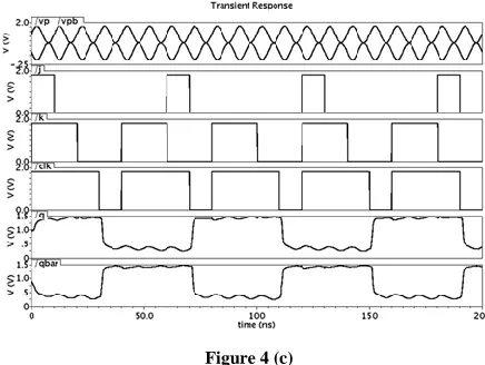
The latches are generally designed by connecting two inverters or two NAND/NOR gates in a cross coupled manner. The proposed EEAL master slave JK flip flop was designed using proposed NAND gates and proposed inverter as shown in figure 4(a). The structure of proposed NAND gate is shown in figure 4(b The inputs are J and K along with the clock signal clk Q and Q are the outputs where Q is the complement of Q The supply voltages are slowly varying complementary split level sinusoidal waveforms (V_P&V P
Q
_
Q J
K clk
Figure4 (a)
A
B
OUTPUT CL
GND P2 P1
T1 T2
N1
N2 Sin
DC
Sin
DC VP
_
VP
Figure 4 (b)
Figure 4 (c)
Figure 4. Proposed EEAL JK flip flop (a) Block diagram,(b) EEAL NAND logic gate (c) Simulation waveform
Table 4(d)
Power Measurement of JK Flip Flop
Circuit
Power consumed (µW)
CMOS JK flip flop
10.22
Proposed JK flip flop
4.39
In order to realize operation of JK flip flop, consider the truth table for JK flip flop. It is required output follow the previous state when both input are „0‟andoutput become complement of previous state when both input are „1‟ Simulated timing waveforms are shown in figure 4(b The combination of inputs at each negative edge of clock pulse 10 01 11 are given in the form of strings The output Q and Q changes according to the inputs at each negative edge of clock pulse Q „1‟ and Q „0‟ when J „1‟ and K „0‟ Similarly Q „0‟ and Q „1‟ when J „0‟ and K „1‟ Output Q will be complemented when J „1‟ and K „1‟ Further the outputs Q and Q are lathed to their corresponding values other than the negative edges of clock pulses.
V. PROPOSED EEALBASED 3-BIT COUNTER
[image:3.612.332.550.137.301.2]International Journal of Emerging Technology and Advanced Engineering
Website: www.ijetae.com (ISSN 2250-2459,ISO 9001:2008 Certified Journal, Volume 5, Issue 3, March 2015)
320
KJ Q
_ Q
Q
_ Q J
K
J
K Q
_ Q 1
1
1
1
1
1
Q0
Q1
Q2
clk
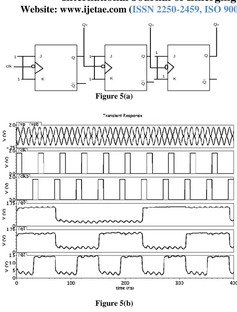
Figure 5(a)
Figure 5(b)
Figure5. Proposed EEAL 3 bit Counter (a) Block diagram, (b) Simulation waveform
Table 5(c)
Power Measurement of 3 bit counter
Circuit
Power consumed (µW)
CMOS counter
16.9
Proposed counter
9.14
Simulated timing waveforms of 3 bit up-counter are shown in figure 5(b). Q2 is always toggle at each negative edge of clock pulse (J and K are high). Q1 is toggle at negative edge of Q2. Similarly Q0 is toggle at negative edge of Q1.The combination of outputs (Q2Q1Q0) at different negative edge of clock pulse is “000,001,010 011 100 101 110 111” This is asynchronous counter thus its delay will be large but due to its simplicity it have been frequently used in literature.
It may be observed that the output waveforms have ripples that are due to the continuous charging and discharging through the sinusoidal type power clocks. The power dissipation due to these ripples or glitches is very small so can be neglected
VI. CONCLUSION
Simulation results obtained from the proposed sequential circuits have got strong validation and give low power dissipation at low frequencies range. The comparison of the proposed circuit with other traditional methodologies has proved that power consumption with the proposed logic is for less as compared to other CMOS circuit. In conclusion, an energy efficient adiabatic technique that would reduce the power consumption. It was found that the proposed adiabatic logic style is advantageous when applied to low-power digital devices operated at low frequencies.. In future these logics can be designed at other technologies to further reduce the power consumption and voltage swing can be improved and further work on minimization of chip area can also be done on various technologies.
REFERENCES
[1] N nuar Y Takahashi T Sekine “ diabatic logic versus CMOS for low power application” IEEE Proc ITC-CSCC2009, july2009, pp.302-305.
[2] Gaurav Singh Ravi Kumar Manoj Kumar Sharma “Comparative Analysis of Conventional CMOS and Energy Efficient Adiabatic Logic Circuits” IJET E Volume3 Issue9 September2013 [3] Mukesh Tiwari, Jai Karan Singh, Yashasvi Vaidhya, “ diabatic
Positive Feedback Charge Recovery Logic for Low Power CMOS Design” IJCTEE Volume2 Issue5 October 2012
[4] Anamika Mishra, Anju Jaiswal, A. Jaiswal K Niketa “Design and Analysis of Conventional CMOS and Energy Efficient Adiabatic Logic for Low Power VLSI pplication” IJE T Volume3 Issue 12 May 2014
[5] P .Vijayasalini. Nirmal Kumar, S.P. Dhivya “Design and analysis of Low power Multiplier and 4:2 Compressor Using diabatic Logic” IJETAE, Volume3, Issue1, Januery2013.
[6] B.Dilli Kumar, M. Bharathi “Design of Energy Efficient Arithmetic Circuits Using Charge Recovery Adiabatic Logic” IJEATAT, volume4, issue1-2013.
[7] M Sowjanya S bdul Malik “Efficiency of diabatic Logic for Low power VLSI Using Cascaded ECRL and PFAL Inverter “IJER Vlume3 Issue4 Jul ug2013
[8] Samik Samanta, Member of IEEE “Power Efficient VLSI Inverter Design Using Adiabatic Logic and Estimation of Power Dissipation using VLSI-ED Tool “IJCCT Volume2 Issue2, 3, 4, 2010. [9] Shipra Upadhyay, RA Mishra, RK Nagaria, SP Singh and Amit
Shukla “Triangular Power Supply Based Adiabatic Logic Family” WASJ, IDOSI, 2013.
[10] J. M. RABAEY, AND M. PEDR M “Low Power Design Methodologies “KluwerAcademic Publishers, 2002
[11] H J M VEENDRICK “Short-circuitDissipation of Static CMOS Circuitry and its Impact on the Design of Buffer Circuits ”IEEE JSSC, pp. 468-473, August 1984
[image:4.612.52.293.115.433.2]International Journal of Emerging Technology and Advanced Engineering
Website: www.ijetae.com (ISSN 2250-2459,ISO 9001:2008 Certified Journal, Volume 5, Issue 3, March 2015)
321
[13] Maksimovic D., Oklobdzija V.G., Nikolic B., Current K.W., “Clocked CMOS adiabatic logic with integrated single phase power clock supply” IEEE Transaction on very large scale integration system, 2000, 8, (4), pp.460-463.
[14] Kramer Denker J S Flower B Moroney J “Second-order adiabatic computation with 2N-2P and 2N-2N-2P logic circuit” Proc. Intern. Symp. Low power design, 1995, pp. 191-196
[15] Hu Jianping; Cen Lizhang; Liu Xiao; “ new type of low power adiabatic circuit with complementary pass-transistor logic” SIC, 2003. Proc. 5th international Conference on Vol.2, Oct.2003, pp.1235-1238,
[16] G Dickinson and J S Denker “ diabatic Dynamic Logic” IEEE Journal of Solid – State Circuits, Vol. 30, No. 03, pp. 311 -315, March 1995.
[17] K Takahashi and M Mizunuma “ diabatic dynamic CMOS logic circuits” IEICE Trans Electron Vol J81CII, Issue 10, pp. 810 -817, October 1998
[18] N. Anuar, Y. Takahashi, T. Sekine, Two phase clocked adiabatic static CMOS logic and its logic, J. Semiconductor Technol. Sci. 10 (1) (2010) 1–10.