Functionality of Self-Seeded
Germanium Nanowires Through
Synthesis Determined Core-Shell
Interface States
Stephen Connaughton
A thesis submitted to the University of Dublin, Trinity College, in application for the degree of Doctor of Philosophy
School of Physics Trinity College Dublin
Declaration
I declare that this thesis has not been submitted as an exercise for a degree at this or any other university and it is entirely my own work.
I agree to deposit this thesis in the University's open access institutional repository or allow the Library to do so on my behalf, subject to Irish Copyright Legislation and Trinity College Library conditions of use and acknowledgment.
taught me over the past 5 years. I would also like to thank Professor John Donegan for his help at the end of my project.
Collaboration is vital in any Ph.D, and especially in this one as I relied on others to provide samples for me. For this reason I would like to sincerely thank Dr. Richard Hobbs, Dr. Olan Lotty and Prof. Justin Holmes. In addition of course I did not work in isolation within the group. Niall Kinahan, Tarek Lutz, Stefan Hansel, Peter Gleeson and Maria Koleśnik all gave me invaluable help during my first years. Great thanks also goes to Olga Varona of Intel, who worked on this project with me for several months. In later years I must thank Eleanor Holmes and Akshara Verma in particular for the regular bitchin’ coffee. A lot of my time in CRANN has been taken up with setting up/fixing/maintaining the machines, and for that Mike Finneran has always offered constant and indispensable help. Finally I am very grateful to Kyle Ballantine, my Mathematica guru.
Great thanks goes to Sinéad, without whose support the past 5 years would have been unbearable, and without whose help this thesis may never have been submitted. I also must thank my parents, Michael and Maureen, who have seen me through 22 long years of school. Perhaps I will get a real job soon. When I think back on my years as a Ph.D. student I will of course always be reminded of José Caridad, who was my collaborator, colleague and friend. I learned a lot from you both in the lab and the pub, much of it still baffling.
Kind thanks goes to various others who have been friends over the years. In particular I would like to thank Brendan and Zara for many fun nights and parties, simply too many to remember. There are some ex-members of the group that I have not yet thanked, but they are certainly not forgotten. Firstly James: I would like to thank you for all of your help as we tried to work out what we were doing in the early days and for the uncountable good memories since the first year of undergrad. The Dooleyfests have been a highlight of the past 5 years. Of course I also couldn’t mention those trips without also thanking Rónán and the eponymous Dooley. To Andrea a.k.a Dj Pani: there are many great nights to thank you for, but I would especially like to thank you and Canly for your hospitality during our trip to Milan. The group was a lot more fun with Robert “prime” in it. I hope that we may find ourselves working together again soon. I feel like I have been accepted as an honorary member of the Duesberg group over the past 2 years. Thanks must therefore go to Toby and Nina especially for the Halloween parties, Niall for the small inland ocean of beer I must owe you, Maria for the various baked goods, Hugo for always bigging up the Bray massive, Kay and Hye-Yong for the house parties and dancing lessons, and also to Christian, Riley, Chanyong and Ehsan. Finally of course thanks to Georg himself for the many stories.
Table of Figures ... vi
List of Tables ... viii
Summary ... ix
1. Introduction ... 1
1.1 Historical context ... 1
1.2 Germanium nanowires ... 5
References ... 8
2. Theory of Electrical Transport in Nanowires ... 11
2.1 Resistivity, Mobility and Basic Measurement Principles ... 12
2.1.1 Definition of Resistivity and Mobility... 12
2.1.1 Measuring Resistivity ... 14
2.1.2 Measuring Field Effect Mobility ... 16
2.2 Electrons in a Periodic Potential ... 20
2.2.1 Bloch Waves ... 20
2.2.2 Parabolic Bands and Effective Mass ... 22
2.2.3 Heavy Holes, Light Holes and the Split off Band ... 23
2.2.4 Non-parabolicity in Nanostructures ... 24
2.2.5 Density of States ... 24
2.3 Origin of Surface States ... 26
2.4 Schottky Barrier ... 28
2.4.1 Origin of Schottky barrier ... 28
2.4.2 Schottky Barrier Height and Fermi Level Pinning ... 30
2.4.3 Modelling Current Flow Through Schottky Barriers ... 34
2.5 Kubo-Greenwood Formula ... 38
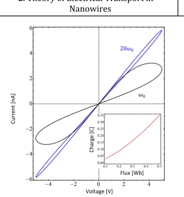
2.6 Memristance ... 41
2.7 Temperature Dependence of the Resistivity of Solids ... 46
2.7.1 Temperature Dependence of Mobility ... 46
2.7.2 Temperature Dependence of the Carrier Concentration ... 47
2.7.3 Variable Range Hopping ... 48
References ... 50
3. Experimental approach ... 53
3.1 Nanowire Material ... 53
3.2 Electrical contacting of single nanowires ... 55
3.2.4 Removal of shell and metallisation for electrical contacting ... 58
3.3 Imaging of nanowires ... 59
3.3.1 Atomic force and optical microscopy ... 59
3.3.2 Scanning electron microscopy ... 59
3.3.3 Transmission electron microscopy ... 60
3.4 Electrical measurement set up ... 62
References ... 64
4. Variation in Electrical Response with Altered Growth Parameters ... 67
4.1 Shell Removal ... 67
4.2 Electrical measurements ... 69
4.3 Memristance model ... 75
References ... 82
5. Diameter Dependence of the Resistivity of Quasi-Metallic Germanium Nanowires 85 5.1 Experimental findings ... 85
5.2 Carrier Concentration and Associated General Resistivity Expressions ... 87
5.2.1 Regime 1: 𝑹 ≫ 𝒅... 88
5.2.2 Regime 2: 𝑹 < 𝒅 ... 90
5.3 Mobility Calculation in Regime 2 (𝑹 < 𝒅) ... 92
5.3.1 Wavefuction of the Charge Carriers ... 93
5.3.2 Fermi Level Position ... 94
5.3.3 Hole-Phonon Scattering ... 95
5.3.4 Coulomb Scattering ... 97
5.3.5 Surface Roughness Scattering ... 100
5.3.6 Details of Calculation ... 100
5.3.7 Origins of the Diameter Dependence of the Resistivity ... 105
5.4 Comparison of Theory and Experiment ... 107
5.4.1 Resistivity in Regime 1 (𝑹 ≫ 𝒅) ... 107
5.4.2 Resistivity in Regime 2 (𝑹 < 𝒅) ... 108
References ... 112
6. Temperature Dependence of Resistance ... 115
6.1 High Resistance Samples with a Gate Effect ... 115
6.1.1 4-Point Data ... 116
6.1.2 2-Point Data ... 119
7. Conclusions and Future Work ... 137
References ... 140
Appendices ... 143
A. Derivation of the Kubo Formula ... 145
References ... 149
B. No Energy Discharge from a Memristive System ... 151
References ... 152
C. Solution of Schrödinger for an Infinite Cylindrical Well ... 153
References ... 157
D. Derivation of Momentum Relaxation Rate due to Phonon Scattering ... 159
C. 1 Acoustic phonon scattering. ... 161
C. 2 Optical Phonon Scattering ... 165
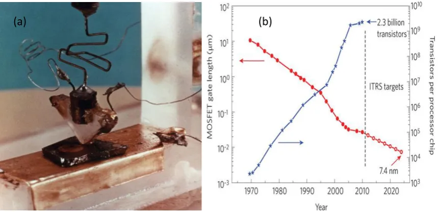
Figure 1.1 (a)A picture of the first transistor ever made. (b)A graph depicting Moore’s
law. ... 1
Figure 1.2 Schematic illustration of the VLS process. ... 4
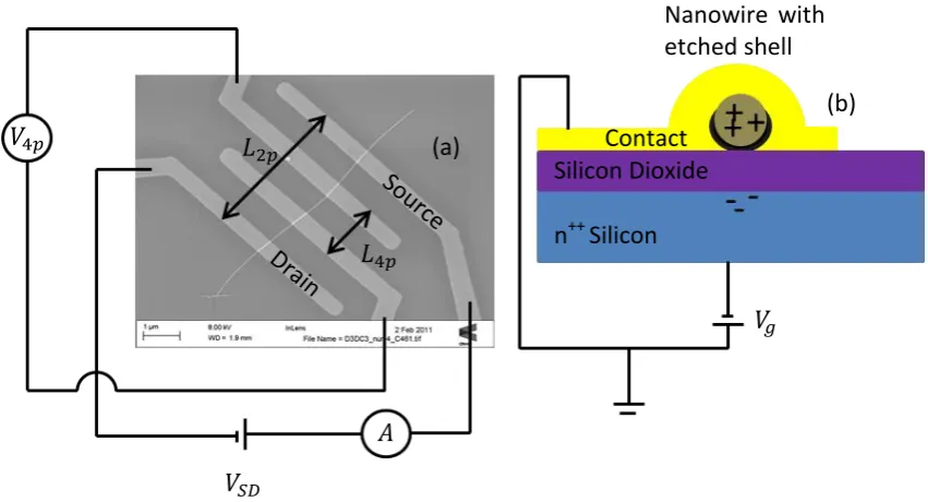
Figure 2.1 Schematic diagram of nanowire field effect transistor ... 16
Figure 2.2 A depiction of the three bands at the top of the valence band in germanium ... 23
Figure 2.3 Representation of the wavefunction at the surface that give rise to surface states. ... 27
Figure 2.4 Schematic depiction of the formation of a Schottky barrier. ... 31
Figure 2.5 Schematic diagram of Schottky barrier formation in the presence of surface states ... 33
Figure 2.6 Examples of theoretical IV curves for Schottky barriers ... 37
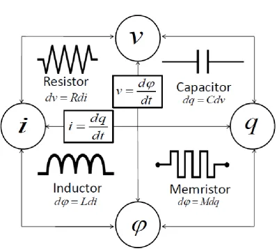
Figure 2.7 Schematic diagram showing the relationships between current, voltage, flux and charge. ... 41
Figure 2.8 A example of a pinched hysteresis loop ... 45
Figure 3.1 TEM image of typical germanium nanowire. ... 54
Figure 3.2 Images of a nanowire field effect transistor being created. ... 57
Figure 3.3 Comparisson of SEM and TEM images of a germanium core. ... 60
Figure 3.4 Circuit diagram of our electrical set up. ... 63
Figure 4.1 SEM image of wires from each batch showing the difference in the damage to the shell... 68
Figure 4.2 Difference in electrical characteristics of wires grown under two different growth conditions. ... 70
Figure 4.3 Extracted conductivity plotted against gate voltage for a wire grown in batch 1 ... 72
Figure 4.4 Schematic diagram of the underlying mechanism of the memristor model . 75 Figure 4.5 Comparisson between memristive device theory and experimentel curves. 79 Figure 5.1 Diameter dependence of the resistivity of batch 2 wires showing little or no gate effect. ... 86
Figure 5.2 Schematic diagram of the volume in which holes are predominantly located for (a) a wire with a diameter above 20 nm (regime 1)and (b) a wire with a diameter less than 20 nm (Regime 2). ... 87
Figure 5.3 Green’s function for Coulomb scattering as a function of radial position in the wire ... 99
Figure 5.4 Position of subband minima and Fermi level as a function of nanowire diameter. ... 102
Figure 5.5 (a) modelled density of states and (b) the average subband bottom’s spacing as a function of wire diameter. ... 103
Figure 5.6 Modelled form factor for scattering from the first to the second subband. 106 Figure 5.7 (a) ratio of space charge region width d to nanowire radius R as a function of diameter (b) comparison between theory and experiment above 20 nm. ... 107
Figure 5.8 (a) Resistivity and (b) mobility calculated from the Kubo-Greenwood formula for wires with diameters from 11 nm to 22 nm. ... 109
electronic devices. While the electrical properties of nanowires grown using a metallic seed as a catalyst have been extensively reported we study self-seeded nanowires in this thesis. Such wires are core-shell in nature and are grown without any intentional doping. Self-seeded nanowires have been previously proposed as an attractive alternative to conventionally grown wires due the alleviation of complications arising from unintentional doping from the metallic seed. The results in this thesis demonstrate that the electrical properties of the self-seeded, core-shell nanowire are dominated by doping from the interfaces states which is in turn dependent on the details of the nanowire growth.
We first examine the room-temperature electrical properties of two sets of wires grown under different growth conditions. A significant difference in electrical behaviour was seen. One batch showed a p-type gate response and memristive behaviour, while the other showed little or no gate effect, and low resistivity. It is proposed that the observed behaviour results from differences in the density of the charge traps located at the interface between the core and the shell of the nanowire, leading to a difference in the nanowire doping. The difference stems from a change in the structural and chemical properties of the shell which is caused by the altered growth conditions. A model is developed in this thesis to explain how the interface states lead to the observed memristive behaviour. In contrast a high density of surface states leads to the observed gate voltage invariance and low resistive response.
diameter of approximately 14 nm. The results are modelled and two separate regimes are found. Above diameters of 20 nm the mobile holes in the wire are confined to an annular region close to the surface of the wire due to the electrostatic attraction of the electrons in the interface states. In this region we model the change in resistivity as resulting from the change in the carrier concentration arising from the difference in scaling between the surface of the wire and the volume of the annular region to which the mobile holes are confined. Below 20 nm diameters we model the mobility using the one-dimensional Kubo-Greenwood formula. Unlike previous applications of this formula to nanowires we take into account explicitly the effects of the aforementioned diameter dependent carrier concentration arising from the surface state doping. The peak-like feature is reproduced by the theory.
1.1Historical context
[image:19.595.106.538.434.642.2]Since the development of the transistor by John Bardeen, Walter Brattain and William Shockley at Bell labs in 1947 semiconductor technology has become central to almost every facet of life. The original transistor was a point contact bipolar junction transistor (BJT), an image of which is shown in Figure 1.1 (a), which was built using a crystal of n -type germanium [1]. Germanium was the focus of much of the early work due to its superb electrical properties. At room temperature the mobility of holes in bulk germanium, 1900 cm2V-1s-1 [2], is the highest of any semiconducting material [3]. It is more than 4 times the value in silicon of 450 cm2V-1s-1 [2]. The electron mobility in germanium is 3900 cm2V-1s-1, which is 2.5 times the value in silicon of 1500 cm2V-1s-1
Figure 1.1 (a)A picture of the first transistor ever made. (b)A graph depicting Moore’s law. In (a) the germanium is the dark material sitting directly under the semi-transparent triangle. Either side of the triangle is covered in a thin film of gold, which has a small gap made in it at the apex of the triangle. The two gold sides are the emitter and collector contacts. At the top of the insulating triangle a spring can be seen which pushes the contacts into the germanium. Underneath the germanium is the metallic gate. (b) shows two versions of Moore’s law. The blue line shows the number of transistors on a single processor chip and the red line shows the gate length of a device from 1970 to 2010. Data points after that are projections. The change in the rate of increase of the number of transistors per chip in 2005 is associated with the introduction of hafnium oxide and the move from geometric to equivalent scaling
group led by Shockley in Bell labs were originally trying to create a field-effect-transistor (FET) [1], a design concept patented as early as 1921 by Julius Edgar Lilienfeld [4]. The first attempts to make such devices proved unsuccessful. This was due to the fact that there exists at the surface of silicon and germanium states that trap mobile electrons and screen out the applied electric field [5]. It was this insight by Bardeen that led the group to develop the point contact BJT, which in fact relied on the existence of such states to operate [1].
The great breakthrough for silicon came in 1959 when it was discovered that a thermally grown layer of silicon dioxide greatly reduced the number of charge traps at the silicon surface [6]. This allowed the development of the first working field effect transistor, the metal-oxide-semiconductor field effect transistor (MOSFET), which was patented in the following year [7]. A thermally grown layer of germanium oxide did not passivate the surface, and so was unsuitable for use in MOSFETs. As MOSFETs were cheaper and easier to produce in integrated circuits than other transistors they became dominant and so too did silicon [8], a fact that remains true to this day.
There are indications that silicon may soon fall out of favour due to the relentless drive towards the miniaturisation of transistors. As famously pointed out by Moore in 1965 [8] the size of a transistor halves approximately every 18 months1. This trend has continued for almost 50 years, as shown in Figure 1.1 (b). This shrinking brought many benefits. Smaller devices were cheaper due to the fact that more could
1 In fact Moore originally stated: “The complexity for minimum component cost has increased at a rate of
time for a charge carrier to traverse the distance from the source to the drain electrode. Transistors followed this trend until about the year 2000, a period of time the international technology roadmap for semiconductors (ITRS) refers to as the “era of geometric scaling” [9]. After this time continued scaling by simply shrinking device lengths was no longer feasible, and we entered an era of “equivalent scaling” [9]. That is to say that the underlying transistor design was changed to bring in device performance enhancements. In the near future this may include changing the channel material from silicon to a high mobility material, such as germanium.
One area that has already undergone significant redesign is the gate oxide. By 2006 the gate dielectric was approximately 1.2 nm thick. Further scaling beyond this was not possible without unacceptably large leakage currents, due to the fact that electrons could tunnel through such a thin barrier. Therefore transistors chip manufacturers changed to using materials with a higher dielectric constant, such as hafnium oxide [10]. Hf02 has a dielectric constant of 25 [11] compared to 3.9 in SiO2 [12], allowing gate control to be maintained with a thicker oxide and was introduced to commercial devices in 2007 by Intel [13]. Germanium nanowire devices with HfO2 dielectrics have already been demonstrated, further suggesting that germanium may be utilised in future electronic devices [14].
suggests that bottom up grown high mobility nanowires may be needed to continue device scaling after 2021 [9].
These technological challenges in the semiconductor industry have spurred research into the growth and characterisation of semiconducting nanowires [15, 16]. This has of course included work on field effect transistors [17-23], but it has also been suggested that nanowires may find a use in optoelectronic [15, 24-28], chemical sensing [15, 29-31] and spin based applications [32-35], for example. In addition the hard confinement of carriers in these structures allow the study of fundamental quantum effects, such as quantised conduction [36, 37] and coulomb blockade [38].
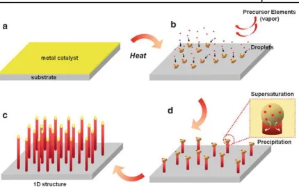
[image:22.595.64.495.61.330.2]Chemically derived semiconducting nanowires are most commonly grown using the vapour-liquid-solid (VLS) mechanism and its related derivatives such as vapour-solid-solid and solution-vapour-solid-solid-vapour-solid-solid. VLS growth was first described in 1964 [39] to explain the growth of silicon whiskers with diameters of the order of microns. In the 90s it was suggested that this mechanism could be used to grow wires with nanoscaled diameters [40, 41]. The starting point of growth for a nanowire using this technique is a metallic seed on the substrate, frequently gold. The substrate is then heated and a gas containing the desired nanowire material is flowed through the chamber. The metallic particles liquefy and absorb the seed material from the vapour until a supersaturated mixture is formed from which the semiconductor precipitates. This is shown schematically in Figure 1.2, which is taken from [42]. The advantage of this technique is that it allows growth of nanowires of a wide range of materials, and allows size control of the nanowires by control of the initial seed diameters and growth times. To make functional nanowire devices it will be necessary to control the doping of the nanowires. This can in principle be achieved by incorporating dopant atoms into the precursor gas from which the nanowire is grown [42]. This is however complicated by the fact that the number of dopants in a wire, 𝑁 has a standard distribution of √𝑁 [43]. For a 10 nm × 10 nm × 1 µm wire with a nominal doping of 1018
fact that seed atoms become incorporated either into or onto the nanowire and can cause unintentional doping [46-52].
A further complication is the surface states that plagued early research into field effect transistors. Due to the high surface to volume ratio of a nanowire these surface effects can dominate the electronic properties of the nanowires. This problem is especially acute in the case of germanium wires due to the high density of surface states – 1014 cm-2 as compared to 1012 cm-2 for silicon for example [53].
As a result there has been a lot of effort put in to determine if the observed electrical properties of germanium nanowires are due to the intentional dopants, unintentionally incorporated seed atoms or surface states. Hanrath et al. [54] grew nominally intrinsic Ge nanowires using a Au seed. The wires showed p-type behaviour when a gate was applied, which was attributed to doping from electron traps at the surface of the wire. Doping from the Au seed was not ruled out however. Wang et al.
However, the effect that the difference in growth conditions had on this density was not discussed.
low resistivity samples show quasi-metallic behaviour in agreement with the results of Chapter 4. Finally Chapter 7 will be present the conclusions and discuss future work.
References
[1] J. Bardeen, Semiconductor research leading to the point contact transistor, Great Solid State Physicists of the 20th Century, (2003) 234.
[2] S.M. Sze, Semiconductor Devices: Physics and technology, John Wiley & Sons, New York, 2002.
[3] R. Pillarisetty, Academic and industry research progress in germanium nanodevices, Nature, 479 (2011) 324-328.
[4] J.S.E. LILIENFELD, Method and apparatus for controlling electric currents, in, Google Patents, America, 1930.
[5] J. Bardeen, Surface States and Rectification at a Metal Semi-Conductor Contact, Physical Review, 71 (1947) 717-727.
[6] M.M. Atalla, E. Tannenbaum, E. Scheibner, Stabilization of Silicon Surfaces by Thermally Grown Oxides*, Bell System Technical Journal, 38 (1959) 749-783.
[7] K. Dawon, Electric field controlled semiconductor device, in: U.P. Office (Ed.), USA, 1963.
[8] G.E. Moore, Cramming more components onto integrated circuits, in, McGraw-Hill New York, NY, USA, 1965.
[9] I. Roadmap, International Technology Roadmap for Semiconductors, 2013 edn, Executive Summary. Semiconductor Industry Association, (2013).
[10] A. Huang, Z. Yang, P.K. Chu, Hafnium-based high-k gate dielectrics, Advances in Solid State Circuits Technologies, (2010) 333-350.
[11] M. Balog, M. Schieber, M. Michman, S. Patai, Chemical vapor deposition and characterization of HfO2 films from organo-hafnium compounds, Thin Solid Films, 41 (1977) 247-259.
[12] S.M. Sze, Physics of Semiconductor Devices, Wiley, New York, 1981.
[13] X. Duan, Y. Huang, R. Agarwal, C.M. Lieber, Single-nanowire electrically driven lasers, Nature, 421 (2003) 241-245.
[14] D. Wang, Y.-L. Chang, Q. Wang, J. Cao, D.B. Farmer, R.G. Gordon, H. Dai, Surface Chemistry and Electrical Properties of Germanium Nanowires, Journal of the American Chemical Society, 126 (2004) 11602-11611.
[15] C.M. Lieber, Nanoscale science and technology: building a big future from small things, Mrs Bulletin, 28 (2003) 486-491.
[16] V.G. Dubrovskii, G.E. Cirlin, V.M. Ustinov, Semiconductor nanowhiskers: Synthesis, properties, and applications, Semiconductors, 43 (2009) 1539-1584.
[17] J. Xiang, W. Lu, Y. Hu, Y. Wu, H. Yan, C.M. Lieber, Ge/Si nanowire heterostructures as high-performance field-effect transistors, Nature, 441 (2006) 489-493.
letters, 6 (2006) 2785-2789.
[20] G. Zheng, W. Lu, S. Jin, C.M. Lieber, Synthesis and Fabrication of High-Performance n-Type Silicon Nanowire Transistors, Advanced Materials, 16 (2004) 1890-1893.
[21] G. Liang, J. Xiang, N. Kharche, G. Klimeck, C.M. Lieber, M. Lundstrom, Performance Analysis of a Ge/Si Core/Shell Nanowire Field-Effect Transistor, Nano Letters, 7 (2007) 642-646.
[22] Y. Li, F. Qian, J. Xiang, C.M. Lieber, Nanowire electronic and optoelectronic devices, Materials today, 9 (2006) 18-27.
[23] J. Goldberger, A.I. Hochbaum, R. Fan, P. Yang, Silicon Vertically Integrated Nanowire Field Effect Transistors, Nano Letters, 6 (2006) 973-977.
[24] Y. Ahn, J. Park, Efficient visible light detection using individual germanium nanowire field effect transistors, Applied Physics Letters, 91 (2007) 162102-162102-162103.
[25] A.B. Greytak, C.J. Barrelet, Y. Li, C.M. Lieber, Semiconductor nanowire laser and nanowire waveguide electro-optic modulators, Applied Physics Letters, 87 (2005) -. [26] S. Gradečak, F. Qian, Y. Li, H.-G. Park, C.M. Lieber, GaN nanowire lasers with low lasing thresholds, Applied Physics Letters, 87 (2005) -.
[27] M. Björk, B. Ohlsson, T. Sass, A. Persson, C. Thelander, M. Magnusson, K. Deppert, L. Wallenberg, L. Samuelson, Nanoletters 2, 87 (2002), Appl. Phys. Lett, 80 (2002) 1058. [28] W. Lu, C.M. Lieber, Nanoelectronics from the bottom up, Nature materials, 6 (2007) 841-850.
[29] F. Patolsky, G. Zheng, O. Hayden, M. Lakadamyali, X. Zhuang, C.M. Lieber, Electrical detection of single viruses, Proceedings of the National Academy of Sciences of the United States of America, 101 (2004) 14017-14022.
[30] F. Patolsky, G. Zheng, C.M. Lieber, Nanowire-Based Biosensors, Analytical Chemistry, 78 (2006) 4260-4269.
[31] G. Zheng, F. Patolsky, C.M. Lieber, Nanowire biosensors: a tool for medicine and life science, Nanomedicine : nanotechnology, biology, and medicine, 2 (2006) 277. [32] E.-S. Liu, J. Nah, K.M. Varahramyan, E. Tutuc, Lateral Spin Injection in Germanium Nanowires, Nano Letters, 10 (2010) 3297-3301.
[33] S.A. Wolf, D.D. Awschalom, R.A. Buhrman, J.M. Daughton, S. von Molnár, M.L. Roukes, A.Y. Chtchelkanova, D.M. Treger, Spintronics: A Spin-Based Electronics Vision for the Future, Science, 294 (2001) 1488-1495.
[34] R. Jansen, Silicon spintronics, Nature materials, 11 (2012) 400-408.
[35] I. Žutić, J. Fabian, S. Das Sarma, Spintronics: Fundamentals and applications, Reviews of Modern Physics, 76 (2004) 323-410.
[36] I. van Weperen, S.R. Plissard, E.P.A.M. Bakkers, S.M. Frolov, L.P. Kouwenhoven, Quantized Conductance in an InSb Nanowire, Nano Letters, 13 (2012) 387-391.
[37] M. Wawrzyniak, J. Martinek, B. Susła, Conductance quantization in nanowires formed at the metal-semiconductor interface, in: Journal of Physics: Conference Series, IOP Publishing, 2009, pp. 012035.
[40] H. Omi, T. Ogino, Self-assembled Ge nanowires grown on Si(113), Applied Physics Letters, 71 (1997) 2163-2165.
[41] A.M. Morales, C.M. Lieber, A Laser Ablation Method for the Synthesis of Crystalline Semiconductor Nanowires, Science, 279 (1998) 208-211.
[42] G.-C. Yi, Vapor–Liquid–Solid Growth of Semiconductor Nanowires, Springer, Berlin Heidleberg, 2012.
[43] T. Mizuno, J. Okumtura, A. Toriumi, Experimental study of threshold voltage fluctuation due to statistical variation of channel dopant number in MOSFET's, Electron Devices, IEEE Transactions on, 41 (1994) 2216-2221.
[44] A.B. Greytak, L.J. Lauhon, M.S. Gudiksen, C.M. Lieber, Growth and transport properties of complementary germanium nanowire field-effect transistors, Applied Physics Letters, 84 (2004) 4176-4178.
[45] P. Xie, Y. Hu, Y. Fang, J. Huang, C.M. Lieber, Diameter-dependent dopant location in silicon and germanium nanowires, Proceedings of the National Academy of Sciences, 106 (2009) 15254-15258.
[46] S. Zhang, E.R. Hemesath, D.E. Perea, E. Wijaya, J.L. Lensch-Falk, L.J. Lauhon, Relative Influence of Surface States and Bulk Impurities on the Electrical Properties of Ge Nanowires, Nano Letters, 9 (2009) 3268-3274.
[47] J. Hannon, S. Kodambaka, F. Ross, R. Tromp, The influence of the surface migration of gold on the growth of silicon nanowires, Nature, 440 (2006) 69-71.
[48] S. Kodambaka, J.B. Hannon, R.M. Tromp, F.M. Ross, Control of Si nanowire growth by oxygen, Nano letters, 6 (2006) 1292-1296.
[49] J.E. Allen, E.R. Hemesath, D.E. Perea, J.L. Lensch-Falk, Z. Li, F. Yin, M.H. Gass, P. Wang, A.L. Bleloch, R.E. Palmer, High-resolution detection of Au catalyst atoms in Si nanowires, Nature Nanotechnology, 3 (2008) 168-173.
[50] M.I. den Hertog, J.-L. Rouviere, F. Dhalluin, P.J. Desré, P. Gentile, P. Ferret, F. Oehler, T. Baron, Control of gold surface diffusion on Si nanowires, Nano letters, 8 (2008) 1544-1550.
[51] S.H. Oh, K.v. Benthem, S.I. Molina, A.Y. Borisevich, W. Luo, P. Werner, N.D. Zakharov, D. Kumar, S.T. Pantelides, S.J. Pennycook, Point defect configurations of supersaturated Au atoms inside Si nanowires, Nano letters, 8 (2008) 1016-1019.
[52] S. Barth, M.M. Koleśnik, K. Donegan, V. Krstić, J.D. Holmes, Diameter-Controlled Solid-Phase Seeding of Germanium Nanowires: Structural Characterization and Electrical Transport Properties, Chemistry of Materials, 23 (2011) 3335-3340.
[53] R.H. Kingston, Review of Germanium Surface Phenemena, Journal of Applied Physics, 27 (1956) 101.
2.1 Resistivity, Mobility and Basic Measurement Principles
In this section we will examine the Drude model of electrical conduction, first proposed by Paul Drude in 1900 [1, 2], 3 years after the discovery of the electron by Thompson [3]. In particular we will examine the definition of electrical resistivity and mobility .We will then examine the methods used to measure resistivity and mobility.
2.1.1 Definition of Resistivity and Mobility
When an electric field, 𝑬 = {𝐸𝑥, 𝐸𝑦, 𝐸𝑧}, is applied to a material the free electrically charged particles in that material will experience a force, 𝑭 = {𝐹𝑥, 𝐹𝑦, 𝐹𝑧}, causing them to drift in the direction of the applied field. We can write [4]:
𝐹𝛽 = 𝑞𝐸𝛽 =
𝑚𝛼𝛽𝑣𝐷,𝛼
𝜏 , Eq. 2.1
where 𝑞 is the charge of the particle, 𝑣𝐷,𝛼 is the drift velocity, 𝜏 is the typical time between scattering events and 𝛼 and 𝛽 are indicies labelling direction, (𝑥, 𝑦, 𝑧). 𝑚𝛼,𝛽 is a component of the second rank mass tensor, relating the component of the field applied in the 𝛽 direction to the component of the drift velocity in the 𝛼 direction 1
.
Eq. 2.1 is the free electron model, where it is assumed that between collisions with the crystal lattice the electron’s movements are unaffected by the presence of the surrounding material. In reality the crystal lattice will create an electric field which will alter the movement of the free electrons. The net effect of this field is included by replacing the mass with the effective mass, 𝑚𝛼𝛽 → 𝑚𝛼𝛽∗ . More details about the
1
The drift velocity of the charge carriers may not be in the same direction as the applied electric field if the crystal is not cubic or there is also an applied magnetic field, for example. In this case the off-diagonal elements of 𝑚𝑖𝑗 will be non-zero. If the drift velocity is in the direction of the applied field the tensors are
effective mass will be given in Section 2.2.2. This is termed the nearly-free electron model [4]. Using this we may rearrange Eq. 2.1 to give:
𝑣𝐷,𝛼 = 𝑞𝜏𝐸𝛽
𝑚𝛼𝛽∗ = 𝜇𝛼𝛽𝐸𝛽, Eq. 2.2
where 𝜇𝛼𝛽 = 𝑞𝜏/𝑚𝛼𝛽∗ is a component of the mobility tensor. The drift velocity is related to the current density as [4]:
𝑗𝛼= 𝑛𝑞𝑣𝐷,𝛼, Eq. 2.3
where 𝑛 is the carrier concentration. The current density is the total current, 𝐼, per cross sectional area, 𝐴. Combining Eq. 2.2 and Eq. 2.3 gives:
𝑗𝛼= 𝑛𝑞𝜇𝛼,𝛽𝐸𝛽 = 𝜎𝛼𝛽𝐸𝛽, Eq. 2.4 where 𝜎𝑖𝑗 is a component of the conductivity tensor, 𝜎̂ [4]. The resistivity tensor, 𝜌̂, is simply the inverse of the conductivity tensor [4]:
𝜌̂ = 𝜎̂−1 = 1
𝑑𝑒𝑡(𝜎̂)𝑎𝑑𝑗(𝜎̂). Eq. 2.5
In our measurements we always measure the current in the same direction as we apply the electric field. As such we measure only one component of the conductivity, resistivity or mobility tensors. For this reason we consider these quantities to be scalar and subsequently drop the subscripts for simplicity 2.
In semiconductors the current will in general be carried by both electrons and holes. The electrons and holes may have different drift velocity, mobility and concentration. All equation given above and subsequent equation derived in the
2
coming sections should therefore contain both electrons and holes. For example Eq. 2.4 is more correctly written as:
𝑗 = 𝑛𝑞𝜇𝑒𝐸 + 𝑝𝑞𝜇ℎ𝐸 = 𝜎𝑒𝐸 + 𝜎ℎ𝐸, Eq. 2.6 where 𝑛 and 𝑝 are the concentration of electrons and holes respectively, and the subscripts 𝑒 and ℎ are used to differentiate between the mobility and conductivity of the electrons and the holes.
The electron and hole concentrations must obey the law of mass action, which states that the product of the electron and hole concentrations must be equal to the intrinsic carrier concentration squared [4]. For germanium the intrinsic carrier concentration is of the order of 1013 cm-3 [4]. We shall show in Chapter 4 that the hole concentration in our nanowires is of the order of 1019 cm-3. This implies that the electron concentration is of the order of 107 cm-3. Due to the fact that there is 12 orders of magnitude difference between the hole and electron concentrations we ignore the holes in our calculations and use the simplified equations as presented in this chapter.
2.1.1 Measuring Resistivity
In practise we do not measure the resistivity of a wire, but rather we measure its resistance, 𝑅. These quantities are related by the active channel length of the device, 𝐿, and the cross sectional area of the wire [4]:
𝑅 =𝜌𝐿
𝐴. Eq. 2.7
𝑉 = 𝐼𝑅. Eq. 2.8 The most basic way to measure the resistance of a nanowire is in a two-point configuration: here two electrical contacts are placed on the nanowire, which we label the source and the drain electrode. A voltage, 𝑉𝑆𝐷, is applied across these two contacts and the resulting current is measured. In this configuration the measured resistance, 𝑅2𝑃, is not the actual resistance of the nanowire, 𝑅𝑁𝑊, but rather this resistance plus the total contact resistance, 𝑅𝐶 [5]:
R2p = VSD
𝐼 = RNW+ RC. Eq. 2.9
𝐼 is the measured current. The active channel length is measured from the outside of
R(NW4p) = V4p
𝐼 . Eq. 2.10
The active channel length for a four point measurement, 𝐿4𝑝, is the distance from the outside of the two inner contacts [6] as shown in Figure 2.1 (a).
2.1.2 Measuring Field Effect Mobility
From Eq. 2.4 it can be seen that:
𝜎 = 𝑛𝑒𝜇, Eq. 2.11
where we now replace 𝑞 with 𝑒, the charge of the electron. In order to extract the mobility in the channel of a field effect transistor the gate is modelled as a capacitor with the gate electrode as one plate and the active channel, in our case the nanowire,
𝑉4𝑝
𝐴
𝑉𝑆𝐷
𝑉𝑔 𝐿2𝑝
𝐿4𝑝 n
++
Silicon Silicon Dioxide
Nanowire with etched shell
Contact (a)
(b)
[image:34.595.66.492.107.337.2]acting as the other plate [5]. This is apparent from the cross section of the device depicted in Figure 2.1 (b). The gate capacitance, 𝐶𝑔 is related to the carrier concentration by:
𝐶𝑔 = 𝑑𝑄
𝑑𝑉𝑔 = 𝐿𝐴𝑒 𝑑𝑛
𝑑𝑉𝑔, Eq. 2.12
where 𝑄 is the charge on each plate of the capacitor, 𝑉𝑔 is a the gate voltage. Differentiating both sides of Eq. 2.11 with respect to the applied gate voltage gives:
𝑑𝜎 𝑑𝑉𝑔 =
𝑑𝑛
𝑑𝑉𝑔𝑒𝜇, Eq. 2.13
where we have assumed that the mobility is constant with the applied gate voltage. Solving this equation for 𝑑𝑛/𝑑𝑉𝑔 and putting it back into Eq. 2.12 we find:
𝐶𝑔 = 𝑑𝜎 𝑑𝑉𝑔
𝐿𝐴
𝜇 . Eq. 2.14
Solving for the mobility gives:
𝜇 = 𝑑𝜎 𝑑𝑉𝑔
𝐴𝐿
𝐶𝑔. Eq. 2.15
In practise we do not measure the conductivity directly, but rather measure the resistance. From Eq. 2.5, Eq. 2.5 and Eq. 2.8 we can write:
𝑅𝑁𝑊 = 𝑉4𝑃
𝐼 = 𝐿
𝜎𝐴 Eq. 2.16
and therefore that:
𝜎 = 𝐼𝐿
These equations are only valid for 4-point measurements, or else the contact resistance must be included. Finally differentiating Eq. 2.17 with respect to the gate voltage and putting the result into Eq. 2.15 we find:
𝜇 = 𝑑𝐼 𝑑𝑉𝑔
𝐿2
𝐶𝑔𝑉4𝑝. Eq. 2.18
This is a more useful equation than Eq. 2.15 as it relates the measured current and 4-point voltage to the mobility. Eq. 2.18 shows that the mobility may be found by measuring the rate of change of the current with the gate voltage with constant source drain voltage applied. This rate of change is known as the transconductance [5]. Equivalently we may measure the conductivity at different gate voltages, calculating the mobility from the slope of the conductivity plotted against the gate voltage, as shown by Eq. 2.15.
The biggest challenge faced in using Eq. 2.12 is correctly determining the gate capacitance. For back-gated nanowires and nanotubes devices a cylinder on plane model is usually used which reads [7]:
𝐶𝑔 = 2𝜋𝜀𝑜𝑥𝜀0𝐿 cosh−1(ℎ + 𝑟
𝑟 )
, Eq. 2.19
where 𝜀𝑜𝑥 and 𝜀0 are the dielectric constant of the gate oxide and of free space, respectively, ℎ is the thickness of the oxide and 𝑟 is the radius of the nanowire. If ℎ ≫ 𝑟 Eq. 2.13 can be simplified to:
𝐶𝑔 = 2𝜋𝜖𝑜𝑥𝜖0𝐿
For our samples this introduces an error of approximately 2 %. Eq. 2.19 is only strictly valid if the oxide completely surrounds the wire, the wire is effectively metallic so that the induced charge resides only on the surface, and the distance between the contacts is infinite so that the distortion of the electric field may be neglected [8]. These assumptions are clearly not valid for a back gated semiconducting nanowire and so the capacitance is normally overestimated, resulting in the measured value for the mobility being too low (see Eq. 2.12) [8].
Furthermore in deriving Eq. 2.12 it is assumed that all the charge induced by the gate is mobile, and so contributes to the current. This will not be the case if there are a large number of charge traps present, such as those located on the germanium surface [9, 10]. In this case at least part of the charge on the gate electrode will be compensated by charges trapped in these surface states which do not contribute to the current flow. This is normally modelled by defining two capacitances, 𝐶𝑖𝑛𝑡 and 𝐶𝑎𝑐𝑐. 𝐶𝑖𝑛𝑡 is the capacitance of the interface and 𝐶𝑎𝑐𝑐 is the capacitance of the free carrier, the subscript standing for accumulation. The two capacitors are connected in parallel, so the total gate capacitance is given by: 𝐶𝑔 = 𝐶𝑖𝑛𝑡+ 𝐶𝑎𝑐𝑐. The final expression for the mobility is then given by replacing 𝐶𝑔 in Eq. 2.12 with 𝐶𝑎𝑐𝑐. This can be written as [11]:
𝜇𝐼𝑛𝑡𝑟𝑖𝑛𝑠𝑖𝑐 = 𝑑𝐼 𝑑𝑉𝑔
𝐿2
𝐶𝑔𝑉𝑆𝑑(1 + 𝐶𝑖𝑛𝑡 𝐶𝑎𝑐𝑐) =
𝑑𝜎 𝑑𝑉𝑔
𝐴𝐿 𝐶𝑔 (1 +
𝐶𝑖𝑛𝑡
surface of the nanowire due to quantum mechanical confinement [11]. If we assume that 𝑡𝑎𝑐𝑐 is 1 nm we find that the term 𝐶𝑖𝑛𝑡/𝐶𝑎𝑐𝑐 = 𝐷𝑖𝑡× 10−14, where 𝐷𝑖𝑡 is in units of eV-1 cm-2.. On the germanium surface the interface trap density has been found to be as large as 1014 ev-1
cm-2 [12], suggesting that the mobility calculated using Eq. 2.12 could be wrong by a factor of 2. Nonetheless the contribution of the surface states to the capacitance is usually ignored due to the fact that 𝑡𝑎𝑐𝑐 is impossible to measure experimentally. We shall also use Eq. 2.12 in analysing our results in Chapter 4, but it is important to remember that in the case where there is a large density of surface states that this represents a lower bound to the true mobility.
2.2Electrons in a Periodic Potential
We shall now develop the theory of electrons in solids arising from quantum theory. Firstly we will look at the origin of Bloch waves, followed by the details of parabolic bands in germanium. The details of the valence band will be described as will the non-parabolic correction necessary in low dimensional structures. Finally we will examine some salient details of the density of states. Many of the equations and ideas from this section will be used in Chapter 5 when we calculate the mobility of our nanowires.
2.2.1 Bloch Waves
Let us assume that we have a particle in a Bravais lattice, defined by a set of points at positions 𝑹. We may then define a set of reciprocal lattice vectors 𝑮, such that 𝑒𝑖𝑮.𝑹= 1. The potential, 𝑉(𝒓), of this lattice will be periodic in real space, 𝑉(𝒓 + 𝑹) = 𝑉(𝒓). We may express the potential as a Fourier expansion in terms of the reciprocal
𝑉(𝒓) = ∑ 𝑉𝑮 𝑮
exp(𝑖𝑮. 𝒓). Eq. 2.22
The wavefunction, Ψ𝐤(𝒓), may in general also be written as a Fourier series in terms of its wavevector 𝒌 [4, 13]:
Ψ𝑘(𝒓) = ∑ 𝐶𝒌 𝒌
exp (𝑖𝒌. 𝒓) Eq. 2.23
where 𝒌 will take a discrete set of values depending on the boundary conditions considered. The time-independent Schrödinger equation is given by [4, 13]:
[− ℏ2
2𝑚∇2+ 𝑉(𝒓)] Ψ(𝐫) = 𝐸Ψ(𝐫), Eq. 2.24 where ∇2 is the Laplace operator, and ℏ is Planck’s constant divided by 2𝜋. To find the allowed values of the coefficients in Eq. 2.23, we put Eq. 2.22 and Eq. 2.23 into Eq. 2.24 resulting in [4, 13]:
∑ℏ
2𝑘2
2𝑚 𝐶𝒌 𝒌
𝑒𝑖𝒌.𝒓+ ∑ 𝐶
𝒌𝑉𝒈𝑒𝑖(𝑮+𝒌).𝒓 = 𝐸 𝒌,𝑮
∑ 𝐶𝒌𝑒𝒊𝒌.𝒓 𝒌
. Eq. 2.25
Due to the fact that 𝑮 is a reciprocal lattice vector and we are summing over all 𝒌 we may replace 𝒌 in the second term of Eq. 2.25 with 𝒌 − 𝑮 [4, 13]3. Doing this and rearranging we find [4, 13]:
∑ 𝑒𝑖𝒌.𝒓[{ℏ2𝑘2
2𝑚 − 𝐸} 𝐶𝒌 𝒌
+ ∑ 𝑉𝑮𝐶𝒌−𝑮] = 0 𝑮
. Eq. 2.26
If this is to be valid at every point in the crystal it must be true for all values of 𝒌. Therefore the term in the square brackets must disappear, giving [4, 13]:
3i.e. ∑ 𝒌 = ∑ 𝒌 − 𝑮
{ℏ 𝑘
2𝑚 − 𝐸} 𝐶𝒌+ ∑ 𝑉𝑮𝐶𝒌−𝑮= 0 𝑮
. Eq. 2.27
This equation defines coefficients that are to be used in Eq. 2.23. It is important to note that the only coefficients that appear here are the ones that differ by an integer number of reciprocal lattice vectors. This allows us to rewrite Eq. 2.23 as [4, 13]
Ψ𝑘(𝒓) = ∑ 𝐶𝑘−𝐺𝑒𝑖(𝒌−𝑮).𝒓 𝑘−𝐺
= (∑ 𝐶𝑘−𝐺𝑒−𝑖𝑮.𝒓 𝐺
) 𝑒𝑖𝒌.𝒓
= 𝑢𝑘(𝒓)𝑒𝑖𝒌.𝒓
Eq. 2.28
The final expression is Bloch’s theorem [14], which states that in any periodic lattice the wavefunction of a single electron will have the form of a plane wave multiplied by a function with the periodicity of the lattice 4.
2.2.2 Parabolic Bands and Effective Mass
Eq. 2.27 can be rearranged to give:
𝐸 =ℏ 2𝑘2
2𝑚 + 𝐶𝒌−1∑ 𝑉𝑮𝐶𝒌−𝑮 𝑮
. Eq. 2.29
If we now examine the case when 𝑉𝐺 ≈ 0, we find that the second term is nearly constant. It is usual to treat it as a constant, 𝐸(𝑀𝑖𝑛,𝑃), with a value equal to its true value at 𝑘 = 0, 𝐸(𝑀𝑖𝑛,𝑃)= 𝐶0−1∑ 𝑉𝑮 𝑮𝐶0−𝑮 [4, 13]. Eq. 2.29 then predicts a parabolic relationship between 𝑘 and 𝐸, which is found to be approximately true near to 𝑘 = 0. The effect of the fact that the second term is not constant is taken into account by replacing the mass with a new effective mass [4, 13]. This is the justification for the
4
The periodicity of 𝑢𝑘(𝒓) can be seen by replacing 𝒓 with 𝒓 + 𝑹,
nearly free electron model that we introduced in Eq. 2.2. Eq. 2.29 can then be rewritten:
𝐸 =ℏ2𝑘2
2𝑚∗ + 𝐸(𝑀𝑖𝑛,𝑃). Eq. 2.30
The effective mass is defined as [4, 13]:
1 𝑚∗=
1 ℏ2
𝑑2𝐸
𝑑𝑘2 Eq. 2.31
which follows from Eq. 2.30.
2.2.3 Heavy Holes, Light Holes and the Split off Band
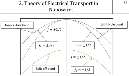
[image:41.595.102.539.39.296.2]In germanium holes have three effective masses associated with them. This is due to the fact that the valence band derives ultimately from a p-orbital with an orbital angular momentum quantum number, 𝑙 = 1 [13]. The total angular momentum quantum number is given by , |𝑙 − 𝑠| < 𝑗 < 𝑙 + 𝑠, where 𝑠 is the electron spin quantum number equal to 1/2 [13]. The total angular momentum is therefore 3/2 or 1/2, giving
Figure 2.2 A depiction of the three bands at the top of the valence band in germanium The split off band has a total angular momentum of 𝑗 = ±1/2 while the heavy and light hole bands have a value of 𝑗 = ±3/2. The split off band lies below the other bands due to spin orbit coupling. The projection of the total angular momentum along the 𝑧 axis is different for the heavy and light hole band, with 𝐽𝑧= ±3/2 and 𝐽𝑧= ±1/2 respectively. At the Γ point both bands are degenerate, but
the degeneracy is lifted away from this point.
Heavy Hole band Light Hole band
Split off band 𝑗 = ±3/2
𝑗 = ±1/2 𝑗𝑧 = ±3/2 𝑗𝑧 = ±1/2
rise to two bands, which we label p1/2 and p3/2. The spin-orbit interaction causes the
p1/2 band to have a lower energy than p3/2 band, and it is therefore called the split-off
band [13]. In germanium the split off band lies 0.295 eV below the p3/2 band [15]. The
projection of the total angular momentum along the 𝑧 axis can take 4 values for the p3/2
band, 𝑗𝑧 = +32, +21, −12, −32. These four bands are degenerate at 𝑘 = 0, but the degeneracy is lifted away from this point [13]. This gives rise to two bands - the heavy hole band with 𝑗𝑧 = ±3/2 and the light hole band with 𝑗𝑧 = ±1/2 [13]. The names are derived from the fact that the effective mass in each band is different. This is depicted in Figure 2.2.
2.2.4 Non-parabolicity in Nanostructures
It is known that for low dimensional systems however that the bands are no longer well described as parabolic, even near 𝑘 = 0, as a result of the raising of the suband edges due to quantum confinement [16]. This is normally accounted for by introducing an extra term, 𝛼, known as the non-parabolicty parameter into Eq. 2.30 [16]:
𝐸 = 𝑈𝑖 +−1 + √1 + 4𝛼 ( ℏ2𝑘2
2𝑚 + 𝐸𝑖
(𝑀𝑖𝑛,𝑃)− 𝑈 𝑖)
2𝛼 ,
Eq. 2.32
where 𝑈𝑖 is the total potential energy in the subband 𝑖. It can be shown that Eq. 2.30 is recovered when 𝛼 → 0. 𝛼 is a material dependent parameter. It takes different values for light holes, heavy holes, holes in the split off band and electrons, as well as depending on energy [17].
2.2.5 Density of States
𝑔𝑚(𝐸) =
𝑉(𝑑𝐸). Eq. 2.33
If the material is modelled as a free electron gas in an infinite potential well the density of states can be calculated to be [13]:
𝑔𝑚(3𝐷)(𝐸) = 2𝜋12(2𝑚∗ ℏ2 )
3/2
√𝐸 Eq. 2.34
in three dimensions and [18]:
𝑔𝑚(1𝐷)(𝐸) = 1 𝜋(
𝑚∗ ℏ2)
1 2
(Θ(𝐸 − 𝐸
(𝑀𝑖𝑛,𝑃))
√𝐸 − 𝐸𝑀𝑖𝑛,𝑃 ) Eq. 2.35 in one dimension 5, where Θ(𝐸) is the Heaviside step function. In one dimension there is an infinity at the minimum of the parabolic band. The emergence of this singularity is important for the discussion of Fermi level depinning in Section 2.4.2.
It should also be noted in both three dimensions and one the density of states is proportional to the effective mass. For this reason the heavy hole band is normally more important than the light hole band in transport, despite the greater mobility of the light holes (see Eq. 2.2 and Section 5.3.6]) [13].
We may also calculate the density of states in one dimension starting from the non-parabolic bands given by Eq. 2.32. In this case we find the following expressions [16, 19]:
𝑘(𝐸) = ℏ−1√2𝑚∗[𝐸 − 𝐸
𝑖(𝑀𝑖𝑛,𝑃)+ 𝛼(𝐸 − 𝑈𝑖)2 Eq. 2.36
𝑣𝑖(𝐸) = 1ℏ𝑑𝐸𝑑𝑘 =[1 + 2𝛼(𝐸 − 𝑈𝑖 ℏ𝑘(𝐸)
𝑚∗ Eq. 2.37
𝑔𝑚(𝑁𝑃)= Θ(𝐸 − 𝐸𝑖
(𝑀𝑖𝑛,𝑁𝑃))2𝑔
𝜋ℏ𝑣𝑖(𝐸) , Eq. 2.38
where 𝑣𝑖(𝐸) is the group velocity of the carrier in subband 𝑖 at energy 𝐸 and 𝑔 is the valley degeneracy. These expressions are valid for either the conduction band or the valance band. In the case of the valance band there are no valleys and so 𝑔 = 1. It should be noted that the effective mass will no longer be constant as the bands are no longer parabolic. The effective mass that appears in Eq. 2.37 is the effective mass for the parabolic band.
2.3Origin of Surface States
The value of the wavevector 𝒌 may be either real or imaginary [20]. If we make the replacement 𝒌 → 𝒌 + 𝑖𝜿in Eq. 2.28, which defines Bloch functions, we find:
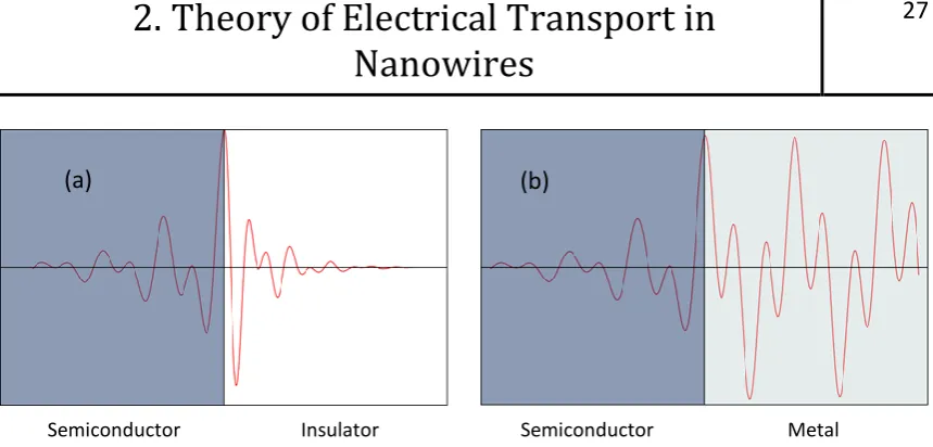
Outside of the crystal the wavefunction may take any form in principle, subject to the requirement that it and its derivative be continuous across the surface. In general this results in wavefunctions with a discreet set of 𝜿 for a given value of 𝒌[21]. If the semiconductor crystal is in contact with an insulator, for example, the wavefunction may join to a corresponding surface state in the band gap of the insulator, decaying exponentially both into the semiconductor and into the insulator. An example of a wavefunction of this type is shown in Figure 2.3 (a). Such states are strongly localised at the interface between the semiconductor and the insulator and are therefore referred to as interface states. For a free semiconductor surface the state on the surface may result from an unsatisfied bond on a surface atom. These are referred to as dangling bonds.
[image:45.595.105.535.42.248.2]In the case that the semiconductor is contacted by the metal the surface states may join to the extended Bloch waves within the metal [21, 22]. Such states are called
Figure 2.3 Representation of the wavefunction at the surface that give rise to surface states. (a) shows the wavefunction at a semiconductor/insulator interface.The wavefunction decays exponentially in both directions away from the interface, resulting in strong localisation of the electron at the interface between the materials. This is the same situation for an intrinsic surface state i.e. at the semiconductor/vaccuum interface. (b) shows a metal induced gap state. On the right an extended Bloch wave in the metal is shown, which decays exponentially in the semiconductor. It is important to note that the wavefunction and its derivitive are continuous at the boundry in both cases and that the periodicity of the Bloch waves in each material is different.
Semiconductor Insulator Semiconductor Metal
metal induced gap states and are often described as the decay of the metal wavefunction into the semiconductor. Metal induced gap states can be either donors or acceptors [20, 21]. In general the states closer to the valence band are donors and those closer to the conduction band are acceptors [21]. The energy at which the states change from being mostly donors to mostly acceptors is known as the charge neutrality level [23, 24]. This energy is important in the discussion of Schottky barrier heights and Fermi level pinning as we shall discuss in Section 2.4.2. If the Fermi level is above this energy the surface will have a net negative charge, or it will be positively charged if it is below it. In germanium the charge neutrality has been measured to be 0.09 ± 0.07 eV above the valence band [23]. Due to the fact that it is so close to the valence band the Fermi level most often lies above it, leading to a negatively charged surface with free holes inside the bulk.
2.4 Schottky Barrier
We will now examine the details of Schottky barriers at metal/semiconductor interfaces. Schottky barriers should play a major role in the determination of the contact resistance of our devices, which we introduced in Section 2.1.1. We will look at the formation of the barriers and then discuss the barrier heights and Fermi level pinning. We will finally look at the way that Schottky barriers are modelled. This discussion will be useful when we develop a model for the memristive response in our devices in Chapter 4.
2.4.1 Origin of Schottky barrier
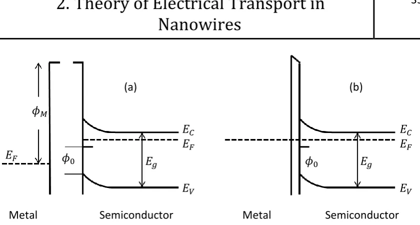
atoms - are isolated from each other, as shown in Figure 2.4 (a). The work function of the metal is the potential required to take an electron from the Fermi level to the vacuum level [25]. It is denoted as ϕm in Figure 2.4. The electron affinity of the semiconductor is the energy between the bottom of the conduction band and the vacuum level at the surface [25], and is shown in Figure 2.4 as 𝜒𝑆. If the metal and semiconductor are connected the thermodynamic requirement for the Fermi level to be equal in the two materials causes charge carriers to flow from the one material into the other [26]. This scenario is shown in Figure 2.4 (b). In the case of an n-type semiconductor electrons will flow from the semiconductor to the metal. These electrons will accumulate in a thin layer at the surface of the metal, typically in a region under a nanometer from the surface [25]. This surface charge on the metal will repel the mobile electrons in the semiconductor, leaving behind a positively charged depletion region at the semiconductor surface. This results in band bending at the semiconductor surface as shown in Figure 2.4 (b). The total charge in the depletion region is directly related to the amount of band bending [25]. In equilibrium the total charge on the metal surface, 𝑄𝑀 must equal the total charge in the depletion region of the semiconductor, 𝑄𝑆 [25]:
𝑄𝑀+ 𝑄𝑆 = 0 Eq. 2.40
while an intimate contact is shown in Figure 2.4 (d). In reality an insulating layer usually exists, but is sufficiently thin that electrons can tunnel through easily. As a result it is usually difficult and unnecessary to distinguish between Figure 2.4 (c) and Figure 2.4 (d) in most practical situations [25]. In Figure 2.4 (d) the barrier height 𝜙𝑏 is shown. It is defined as the difference between the bottom of the conduction band at the surface and the Fermi level [25].
2.4.2 Schottky Barrier Height and Fermi Level Pinning
In 1939 Schottky and Mott proposed that the barrier height should be given by [25]:
𝜙𝑏 = 𝜙𝑀− 𝜒𝑆 Eq. 2.41
for the case of an n-type semidunductor. With reference to Figure 2.4 it is then easy to see the origin of Eq. 2.41, if we remember that as 𝛿 → 0 the voltage drop must also disappear [25]. For a p-type semiconductor the corresponding equation is [25]:
ϕb=Eg− (ϕM− 𝜒𝑆), Eq. 2.42
where Eg is the band-gap of the semiconductor. Eq. 2.41 and Eq. 2.42 suggest that the
barrier height for any given semiconductor should be entirely determined by the work function of the contacting metal. In many cases however it was found that the barrier height was in fact independent of the metal used [27]. This fact was explained by Bardeen in 1947 as resulting from the existence of surface states on the semiconductor [27].
resulting from a depletion region in the semiconductor. In the presence of charged surface states however, we must include the surface state charge, 𝑄𝑆𝑆, as well. The neutrality condition that must be met is then [25]:
𝑄𝑚+ 𝑄𝑆𝑆+ 𝑄𝑆 = 0 Eq. 2.43
Figure 2.4 Schematic depiction of the formation of a Schottky barrier. (a) shows the situation when the metal and the semiconductor are seperated by a large distance. The work function of the metal and the electron affinity of the semiconductor are shown, as are the position of the bottom of the conduction band, 𝐸𝐶, the top of the valence band 𝐸𝑉 and the Fermi level 𝐸𝐹 in both
materials. An n-type semiconductor is shown. (b) depicts the situation after electrons are alowed to freely move between the two materials, such as through the connecting wire shown at the bottom of the image. The transfer of charge from the semiconductor to the metal causes the Fermi level to be constant throughout the entire device. The resulting voltage drop across the interface is shown. (c) shows the situation when the seperation between two surfaces is greatly reduced, and (d) depicts intimate contact. (c) may be the most physically relevent situation as a thin layer of oxide often resides on the semiconductor surface. The barrier, 𝜙𝐵 is indictaed in (d).
Metal Metal Metal Metal Semiconductor Semiconductor Semiconductor Semiconductor
𝜙𝑀 𝜙𝑀
χ𝑆 χ𝑆 χ𝑆 𝜙𝐵 𝐸𝐹 𝐸𝑉 𝐸𝐹 𝐸𝑉 𝜙𝑀 𝛿 𝑉𝑖
(a) (b)
(c) (d)
[image:49.595.106.532.38.489.2]As we discussed in Section 2.3 there exists an energy in the band gap known as the charge neutrality level. It is usual to define the height of the charge neutrality level relative to the top of the valence band as we have shown Figure 2.5. If this coincides with the Fermi level the surface is neutral [21]. In the case where the Fermi level is above the charge neutrality level the surface will have a negative charge. This situation is depicted in Figure 2.5. In Figure 2.5 (a) we depict the bands of the semiconductor surface and metal surface when there is a large gap between the two materials, just as we did in Figure 2.4 (a). We are effectively setting 𝑄𝑀 = 0 in Eq. 2.43. Due to the fact that the surface is negatively charged, there must exist a depletion region with associated band bending to satisfy the neutrality condition (Eq. 2.43), even in the absence of a metal contact [27]. When the metal and semiconductor are brought into contact the Fermi levels must align due to the transfer of electrons from the semiconductor to the metal just as they did in the case without surface states. In this case however the electron may originate from a surface state. If this happens the term 𝑄𝑀 + 𝑄𝑆𝑆 in Eq. 2.43 will be unchanged and so there does not need to be an increase in
can be deduced from this image that in the case of perfect Fermi level pinning the height of the barrier is given by [27]:
𝜙𝑏 = 𝐸𝑔− 𝜙0 Eq. 2.44
where 𝐸𝑔 is the band gap. This limit may be practically reached if as few as one in every 100 surface atoms contributes a surface state [27].
Fermi level pinning is also the phenomenon that reduced the gate effect in MOSFETs in the presence of surface states as discussed in Section 1.1. A MOSFET works on the principle that a charge on the gate electrode is compensated by an equal but opposite charge in the semiconductor, which alters the resistivity of the semiconductor (see Eq. 2.4 and Section 2.1.2). In the presence of surface states the charge will be at least partially compensated by immobile charges on the surface, which do not contribute to the current [10]. Equivalently we may say that the Fermi level is pinned
𝜙𝑀
𝜙0
𝐸𝐹 𝐸𝐹
𝐸𝐶
𝐸𝑉
𝐸𝐹 𝐸𝐶
𝐸𝑉 𝜙0
Semiconductor Metal Semiconductor
Metal
𝐸𝑔 𝐸𝑔
Figure 2.5 Schematic diagram of Schottky barrier formation in the presence of surface states In both diagrams the top of the valence band, 𝐸𝑉, the bottom of the conduction band, 𝐸𝐶, the Fermi
level, 𝐸𝐹, the band gap, 𝐸𝑔, and the charge neutrality level, 𝜙0 are indicated. (a) shows the bands
when the metal and the semiconductor are separated. The work function of the metal, 𝜙𝑀 is
shown. The bands in the semiconductor are bent at the surface due to the negative charge in the surface states that results from the Fermi level being above the charge neutrality level. In (b) we show the bands after the metal and semiconductor are in close contact, analogous to Figure 2.4 (c). We have shown the extreme case with the density of surface states near to infinity. Due to this the band bending at the edge of the semiconductor which gives rise to the Schottky barrier is unaffected by the addition of the metal.
[image:51.595.110.530.47.272.2]by the surface states and cannot be changed by the gate. We will see in Chapter 4 that we observe such an effect in some of our wires.
It has been claimed that in the case of nanostructures Fermi level pinning should be alleviated [28]. An experimental demonstration of this has recently been reported [6]. This arises from the fact that in one dimension the density of states goes to infinity for certain energies, as discussed in Section 2.2.5. As a result the density of states of free carriers in the semiconductor is greater than the density of trapped surface states and the above argument no longer holds. We note however that it is theoretically predicted that the pinning will only be significantly alleviated if there are fewer than one surface state per ten surface atoms for a wire with a 6 nm diameter [28]. As our wires have diameters from 10 to 25 nm we expect that fewer surface states will be necessary for pinning to occur. We will argue in Chapter 4 that the density of trap states at the core/shell interface is close to the density of surface atoms in our devices, meaning Fermi level pinning may occur here. This will be further discussed in Chapter 6.
2.4.3 Modelling Current Flow Through Schottky Barriers
The current flow through a Schottky barrier is ideally given by the equation [25]:
𝑗 = 𝑗0exp ( 𝑞𝑉
𝑘𝐵𝑇) Eq. 2.45
mechanisms [25]. The first is the diffusion of the electrons across the depletion region at the surface of the semiconductor. This gives rise to the diffusion model, which gives [25]:
𝑗0 = 𝑞𝑁𝐶𝜇𝐸𝑀𝑎𝑥exp (− 𝑞𝜙𝑏
𝑘𝐵𝑇), Eq. 2.46
where 𝑁𝐶 is the effective density of states in the conduction band of the semiconductor, 𝜇 is the mobility of the semiconductor perpendicular to the surface and 𝐸𝑀𝑎𝑥 is the maximum electric field in the barrier. It should be noted that 𝐸𝑀𝑎𝑥 depends on the magnitude of the applied voltage [25]. As a result 𝑗0 is not constant, and so the Schottky barrier is not ideal.
An alternative model for a Schottky barrier is the thermionic emission model. Here it is assumed that the current limiting process is the transfer of the electrons across the metal-semiconductor interface [25]. In this case we may write [25]:
𝑗0 = 𝐴∗𝑇2exp (− 𝑞𝜙𝑏
𝑘𝐵𝑇), Eq. 2.47
𝜂 = 1 − ( 𝑏
𝑑𝑉). Eq. 2.48
Eq. 2.48, Eq. 2.47 and Eq. 2.48 can be combined to give:
𝑗 = 𝐴∗𝑇2exp (−𝑞𝜙𝑏(0)
𝑘𝐵𝑇 ) exp ( 𝑞𝑉
𝑘𝐵𝑇), Eq. 2.49
where 𝜙𝑏(0) is the barrier height with no applied voltage. An ideal Schottky barrier can be recovered by setting 𝜂 = 1 which is equivalent to setting the barrier height to be independent of the applied voltage as can be seen from Eq. 2.48.
The length of the diffusion region is typically of the order of 1 µm [25]. As this is much longer than the width of the nanowire, it is likely that the depleted region is curtailed in the nanowires. As a result the main barrier to current flow will be emission across the barrier. It is therefore expected that thermionic emission theory is most applicable in the case of nanowires [25, 29].
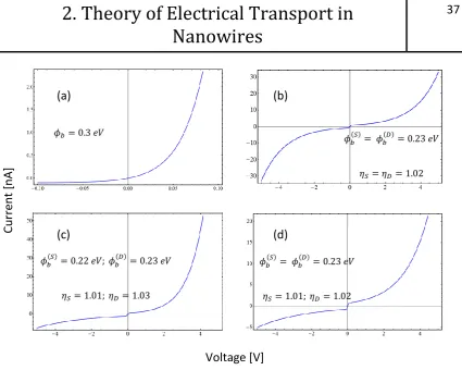
In our devices we will have not one, but two Schottky barriers – one at the source and one at the drain. For the case of ideal back to back Schottky barriers the current is given by [29]:
𝑗 = 𝐽𝑆 𝐽𝐷sinh ( 𝑞𝑉 2𝑘𝐵𝑇) 𝐽𝑆exp (2𝑘𝑞𝑉
𝐵𝑇) + 𝐽𝐷𝑒𝑥𝑝 (− 𝑞𝑉 2𝑘𝐵𝑇)
, Eq. 2.50
where 𝐽𝑆,𝐷 = 𝐴∗𝑇2exp (−𝑞𝜙𝑏
(𝑆),(𝐷)
𝑘𝐵𝑇 ) and 𝜙𝑏
(𝑆)
and 𝜙𝑏(𝐷) are the barrier heights at the source and drain respectively when the thermionic emission model is used. The non-ideality of the barriers is introduced by replacing 𝜙𝑏(𝑆),(𝐷) as [29]:
(a)
𝜙𝑏(𝑆)= 𝜙𝑏(𝐷)= 0.23 𝑒𝑉
𝜂𝑆= 𝜂𝐷= 1.02
(d) (b) (c) Voltage [V] Cur re n t [n A]
𝜙𝑏(𝑆)= 0.22 𝑒𝑉; 𝜙𝑏(𝐷)= 0.23 𝑒𝑉
𝜂𝑆= 1.01; 𝜂𝐷= 1.03
𝜙𝑏(𝑆)= 𝜙𝑏(𝐷)= 0.23 𝑒𝑉
𝜂𝑆= 1.01; 𝜂𝐷= 1.02
[image:55.595.109.535.38.378.2]𝜙𝑏= 0.3 𝑒𝑉