International Journal of Emerging Technology and Advanced Engineering
Website: www.ijetae.com (ISSN 2250-2459,ISO 9001:2008 Certified Journal, Volume 2, Issue 12, December 2012)
11
Simulation Implementation of Microstrip Antenna Array for
1.8GHZ Band With 10DB Gain
G.C NWALOZIE
1, V. N OKOROGU
2, A.C OKAFOR
3, V. E OWEH
41, 2, 3,Electronic and Computer Engineering Department, Nnamdi Azikiwe University Awka, Nigeria 4Computer Engineering Department, Delta State Polytechnique, Oghara, Nigeria
Abstract-- Microstrip patch antennas are versatile in terms of their geometrical shapes and implementation. The light weight construction and the suitability for integration with microwave integrated circuits are two more of their numerous advantages. Additionally the simplicity of the structures makes this type of antennas suitable for low-cost manufacturing. And this is also one key feature why microstrip patch antennas are used in mobile communication applications. Inhibiting characteristics of a single microstrip patch, like low gain and smaller bandwidth, make it more necessary for array configuration. In this work the design and simulation of microstrip patch antenna array was done. The design involved 1- patch, 4 x 1 liner arrays, with an element spacing of a half of a free space wavelength. The antenna was designed to operate at 1.8GHz band, which is almost standard for base station applications. The simulation was developed in MATLAB and Transmission line Matrix (TLM) was used for the model
Keywords-- Antenna array, patch antennas, directivity and gain
I. INTRODUCTION
In recent years, there has been rapid growth in wireless communication. With the increasing number of users and limited bandwidth that is available, operators are trying hard to optimize their network for larger capacity and improved quality coverage [1].
This surge has led the field of antenna engineering to constantly evolved and accommodate the need for wideband, low cost, miniaturized and easily integrated antennas [1]. The quest to solve these problems led to the study of microstrip antennas. The microstrip patch antennas are associated with several advantages of being low profile, versatile, conformal and low-cost devices. The advantages of microstrip antennas make them suitable for various applications like, vehicle based satellite link antennas [2], global position systems (GPS), radar for missiles and telemetry [3] and mobile handheld radios or communication devices. The Microstrip Antennas (MSAs) are low profile, mechanically robust, inexpensive to manufacture, light weight and ability of integration with electronic or signal processing circuitry.
With respect to radiation properties, microstrip antennas are versatile in terms of resonant frequencies, polarization, pattern and impedance. They allow the use of additional tuning elements like pins or varactor diodes between the patch and the ground plane.
Designing active/passive microwave circuits, on the other hand, requires understanding of both mathematical relations (i.e. theory) and application (i.e. Computer simulations as well as measurements). Mathematical relations exist for only simple, idealized microstrip structures and may help to understand the fundamentals. Fortunately, powerful numerical simulation methods are available which can be used to design complex microstrip. Among the others are the finite difference time domain (FDTD), the transmission line matrix (TLM), the finite element method (FEM), and method of moments (MoM).
In [4], Johan Lagerquits analyzed and designed “An Electrically steerable Microstrip Antenna for Ground to Air use”, this is a single-feed polarized microstrip antenna array, operating at 2.45GHz. The antenna was intended to be used for reception of a video signal transmitted from an unmanned aircraft, but can be used for other applications as well. Due to the fact that it was supposed to be used in a switched system, the beam width was quite narrow. Measurements of the antenna showed that it had a half power beam width of 40o for a VSWR lower than 1.5 and an axial ratio lower than 3dB, the bandwidth was 80MHz centered at 2.44GHz.
International Journal of Emerging Technology and Advanced Engineering
Website: www.ijetae.com (ISSN 2250-2459,ISO 9001:2008 Certified Journal, Volume 2, Issue 12, December 2012)
12
Adil Hameed and Basin Jarialla [6] reported in “Design and simulation of Broadband Rectangular Microstrip Antenna”.In this work, many techniques were suggested and analyses for rectangular microstrip antenna (RMSA) operating in X-band for 10GHz centered frequency. The design of the RMSA was made to several dielectric materials and the selection was based upon which material gives a better antenna performance with reduced surface wave loss. Duroid 5880 and Quartz are the best materials for the design to achieve a broader bandwidth (BW). The overall antenna BW for RMSA was increased by 11.6% with Duroid pin (Reactive loading), while for Quartz 17.4%. Modification of patch shape with similar improving techniques gave an overall increasing VSWR bandwidth of 26.2% for Duroid 5880 and a bandwidth of 30.9% for Quartz.
[image:2.612.340.561.260.388.2]This work describes the design and simulation of rectangular microstrip patch antenna array for the wireless communication systems which operates at 1.8GHz band. The antenna is modeled using the TLM model. The simulation is developed in MATLAB with the specifications shown in the table below.
Table 1
Array Antenna Specifications
Features Required Values
Centre Frequency 1.8.GHz
Array Antenna
Configuration
Liner Array
Microstrip Radiator used Rectangular Patch
Polarization Linear
Antenna Gain ≥ 10dB
Antenna impedance BW ≥ 5%
II. STRUCTURE OF AMICROSTRIP ANTENNA
In its basic form, microstrip antennas are similar to parallel plate capacitors. Both have parallel plates of metal layer and a sandwiched dielectric substrate between them. But in microstrip antenna, one of these metal plates is infinitely extended than the other, to form the ground plane; whereas the smaller metal plate is described as radiating patch.
Since the size of the patch is often proportional to frequency of the propagating signal, this class of antenna is classified as resonant antennas. This contributes to the basic shortcoming of the microstrip antennas related with its narrow bandwidth, usually only a few percent [1] of the resonant frequency. So far, several shapes of microstrip patches, such as rectangular, circular, triangular, semicircular, sectoral and annular etc, are successfully used as radiating antenna elements employed various communication control devices.
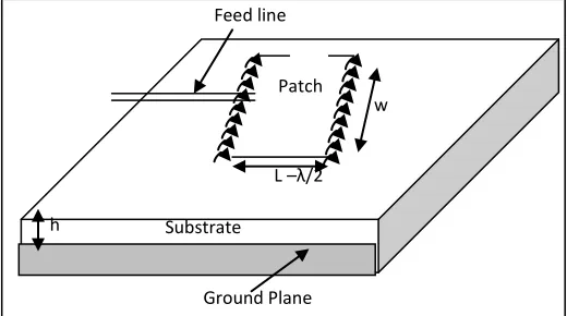
Fig 1 Microstrip rectangular patch antenna
When the patch is excited by a feed line, charge is distributed on the underside of the patch and the ground plane. At a particular instance of time the attractive force between the underside of the patch and the ground plane tend to hold a large amount of charges to the edge of the patch, creating a large density of charge at the edges. These are the sources of fringing field. Radiation from the microstrip antenna can occur from the fringing field between the periphery of the patch and the ground plane [1]. Assuming no variations of the electric field along the width (w) and the thickness (t) of the microstrip structures, the electric field excited by the patch is shown in fig 2.
[image:2.612.317.577.558.703.2]
Figure 2 radiation mechanism associated with microstrip patch
Patch
h
Ground Plane
h Substrate
Ground Plane
w
L –λ/2
Patch
International Journal of Emerging Technology and Advanced Engineering
Website: www.ijetae.com (ISSN 2250-2459,ISO 9001:2008 Certified Journal, Volume 2, Issue 12, December 2012)
13
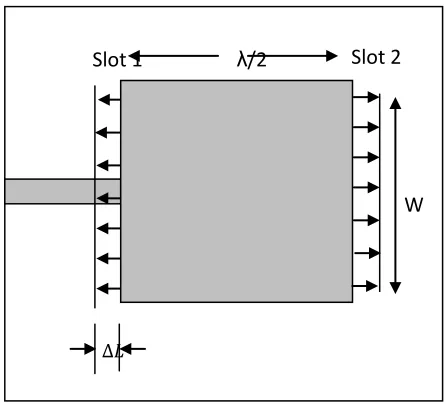
[image:3.612.52.275.296.500.2]Radiation is ascribed mostly to the fringing field at the open circuited edge of the patch length. The fields at the end can be resolved into normal and tangential components with respect to the ground plane. The normal components are 180o out of phase because the patch is λ/2 long; therefore the four field radiation produced by them cancels in the broadside direction [2], the tangential components (those parallel to the ground plane) are in phase, and the resulting field combine to give minimum radiated field normal to the surface of the structure i.e., broadside direction. Therefore, the patch may be represented by two slots λ/2 apart as shown in figure below, excited in phase and radiating in the half space above the ground plane.
Fig 3 Increase in length of the microstrip patch
Typically, to excite the fundamental TEM mode, the length L of the rectangular patch remains slightly smaller than λ/2, where it is the wavelength in the effective dielectric medium [3]. In terms of free space wavelength (λ), is expressed by [3]
(1)
Where is the effective dielectric constant of a
microstrip line and is given as
* + (2)
The value of stays between 1 (dielectric constant of
air) and the dielectric constant of the substrate , because the electromagnetic fields by the microstrip reside partially in the air and partially in the substrate.
However, to enhance the electromagnetic (EM) field in the air, which account for radiation, the width (W) of the patch needs to be increased. Radiating EM fields can also be enhanced by decreasing the or by increasing the substrate thickness (h). It is of note that, since „W‟ and „h‟ is constrained by the input impedance and unwanted-surface-waves respectively. A compromise is required while selecting antenna dimensions. Since microstrip patches are often fed or integrated with microstrip transmission-lines or circuits, the requirement of these devices are also important.
The microstrip antenna can be excited or fed directly either by coaxial probe or by a microstrip line. It can also be indirectly using electromagnetic coupling (proximity) or by aperture coupling method, in which there are no direct metallic contact between the feed line and the patch. Since feeding techniques influences the input impedance, it is often exploited for matching purposes. Also as the antenna efficiency depends on the transfer of power to the radiating element, feeding technique plays a vital role in the design process
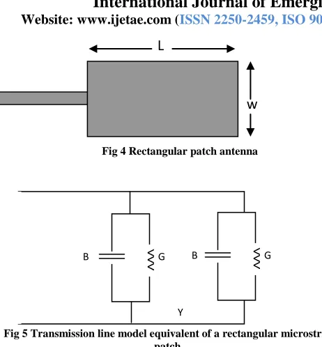
There are many methods of analysis of microstrip antennas. The most popular methods are based on the transmission line model, cavity model and full wave analysis. In this work, transmission line model is used to calculate the dimensions and input impedance associated with the radiating patches.
The transmission line model (TLM)
Although the transmission line model yields less accurate results, it is a very simple model and provides a good physical insight of the basic antenna performance. In this model, the microstrip patch element is viewed as a transmission line resonator with field only varying along the length (no transverse field variations), and the radiation occurs mainly from the fringing fields at the open circuited ends. The patch is represented by two slots that are spaced by length of resonator.
This model was originally developed for rectangular patches but has been extended for generalized patch shapes. Many variations of this model have to been used to analyze the microstrip antenna [7], since the normal analysis was derived for rectangular patch, some authors [8] have modified it to suite other patch shapes like rectangular, and others have modified it to suit to triangular patch shapes[9].
Slot 1
Slot 2
W
International Journal of Emerging Technology and Advanced Engineering
Website: www.ijetae.com (ISSN 2250-2459,ISO 9001:2008 Certified Journal, Volume 2, Issue 12, December 2012)
[image:4.612.48.279.111.360.2]14
Fig 4 Rectangular patch antenna
Fig 5 Transmission line model equivalent of a rectangular microstrip patch
The given parameters for the antenna design are as follows:
= Operating frequency = 1.8GHz
= relative primitively (i.e. dielectric constant) of the substrate
(here =2.2 for duroid 5880 substrate)
h = substrate height = 1.6mm
At low frequencies, remains constant and can be
expressed in terms of patch dimensions and substrate dielectric constant ( , according to equation (2)
Also, due to the fringing effect, the electrical length of the patch increases by a distance of 2 ∆L, as illustrated in figures 4
In transmission line model, ∆L, is expressed as
( )( )
( )( ) (3)
∆L = fringe factor
The width can be calculated thus
( ) (4)
C is the velocity of Electromagnetic wave (C=3*108m/s).
Equally Le which is the effective length of the patch is
given as
(5)
Therefore patch length L is given as,
L = Le - 2∆L (6)
The input impedance should be accurately known so that a good match between the element and the feed can be designed.
For a rectangular patch, typical input impedances at the edge of a patch range from 100Ω to 400Ω, and can be approximated as follows [1],
* + (7)
Now, as operating frequency increases, effective dielectric constant (εeff) increases and eventually
approaches the value of substrate dielectric constant (εr).
A microstrip antenna is basically a broadside radiator, which has a relatively large beam width and low gain characteristics. The formula for the E and H - Plane radiation pattern are given by [10],
E – plane
( ) * ( ) + ( )
* + (8)
H – plane
( ) * ( ) +
* + (9)
Where is the free space waver number and
is the operating wavelength.
The half power beam widths in the H and E planes are given by,
*
( )+ (10)
[
( )] (11)
Thus beamwidth can be increased by choosing a smaller element, thus reducing W and L. For a given resonant frequency, these dimensions may be changed by selecting a substrate having a higher relative permittivity. As beamwidth increases, elements gain and directivity decrease, however, efficiency is unaffected.
The expression for approximately calculating the directivity D of the rectangular microstrip antenna is given by,
( ) (12)
The antenna gain which is a product of directivity and efficiency can be approximated thus,
Gain= (13)
w
L
<
<
<
<
<
<
<
<
<
<
<
<
<
<
<
<
<
<
<
<
<
<
<
<
<
<
<
<
<
<
B G B G
International Journal of Emerging Technology and Advanced Engineering
Website: www.ijetae.com (ISSN 2250-2459,ISO 9001:2008 Certified Journal, Volume 2, Issue 12, December 2012)
15
ε is the efficiency is given as
( ) (14)
Psp is the space wave power and Psur is the surface wave
power
Gain (dB)
(15)
A = L x W
The most serious limitation of the microstrip antenna is its narrow bandwidth (BW). The BW could be defined in terms of its VSWR or input impedance various with frequency or in terms of radiation parameters. For the circularly polarized antenna, BW is defined in terms of the Axial Ratio.
VSWR is a very popular parameter for determining the BW of a particular antenna configuration (1≤VSWR ≥ 2) is an acceptable interval for determining the BW of the antenna.
BW is represented more concisely as a percentage where:
BW% = (16)
Where ∆f is the width of the range of acceptable frequencies, and fo is the resonant frequency of the antenna
[12].
III. ARRAY DESIGN
Any antenna array can be factored into two components. One component, , contains the field pattern of a
single radiating element and the second component, array factor AF, that contains geometric information concerning how the antennas are arranged.
∑ (17)
The importance of this separation of terms is the fact that the array pass band and stop band can be designed by controlling both the amplitude and phases of the array factor. The element field pattern then only affects the angle at which the pass band can be placed and the directivity of the overall array pattern.
The relative spacing between elements are essential in shaping the radiation pattern of the array antenna.
The array factor for any N-element array is given by
∑ ( ) (18)
Where ψ = kdcosθ + β = 2πd/λ cosθ + β
From this equation it is evident that the excitation. Phase (≈β), and the excitation amplitude (≈an) are
importance factors (among others) to influence the radiation characteristic of the designed array antenna. For uniform linear array the amplitude an is 1 for all elements.
This study concentrates on broadside linear array that does not require phase shift; therefore β can be eliminated from the equation.
The gain of a single patch (in dB) is a factor element:
gain of antilog10Gain=Gain (not in dB)
The array gain for equally weighted and phased elements is equal to the number of elements, for N- element.
G array = N x (antilog of single patch gain) (19) The effective area can be approximated as:
Gain =
Where A is the effective area.
When two or more radiating patches are near each other, they interfere with each other depending on; radiation characteristic of each, relative separation between them and relative orientation of each antenna. This interference of energy is known as mutual coupling. Due to the significant contribution of this factor in the antenna performance, it must be difficult to predict analytically, but using fully-wave analysis which is beyond the scope of this work, it can be easily incorporated in the array design.
Mutual coupling is primarily attributed to the fields that exist along the air-dielectric interface. So by selecting the correct distance, these fields can be decomposed to constructive space waves or destructive surface waves. The spacing at which one plane coupling overtakes the other one also depends on the electrical properties and the geometrical dimensions of the microstrip antenna. The spacing of elements is usually 0.5λ ≥ d ≥ λ.
IV. SIMULATION IMPLEMENTATION AND RESULTS
The implementation is done by using a simulation package (MATLAB), and the results obtained are presented below.
The transmission line method was used for calculation of patch dimensions, and other antenna parameter such as gain, bandwidth, efficiency, impedance, etc. were calculated.
International Journal of Emerging Technology and Advanced Engineering
Website: www.ijetae.com (ISSN 2250-2459,ISO 9001:2008 Certified Journal, Volume 2, Issue 12, December 2012)
[image:6.612.45.293.149.632.2]16
Table ii
Rectangular microstrip patch specification.
Features Required Value
Frequency (GHz) 1.80
Dielectric constant 2.20
Width (mm) 65.88
Length (mm) 56.14
Height (mm) 1.60
Rad resistance (Ohm) 2000
Input Impedance (Ohm) 283
Efficiency 0.99
Gain (dB) 5.6
Directivity (dB) 6.94
[image:6.612.41.296.163.601.2]
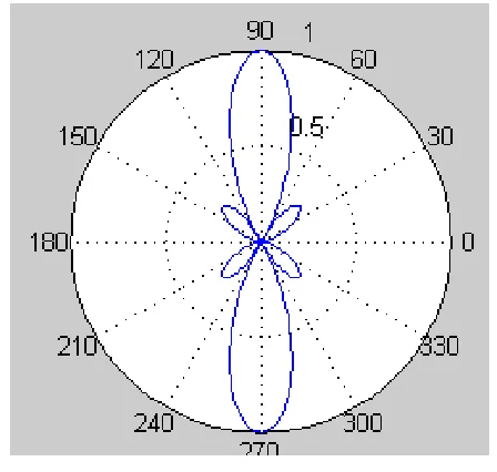
Figure 6. Radiation pattern of a microstrip patch
From the figure above, it can be seen that the designed antenna has a large beamwidth with sidelobes. The gain is 5.6 dB
[image:6.612.332.556.175.388.2]But using a uniform linear array with four elements and interelement spacing of 0.5𝛌, and operating frequency of 1.8GHz our desired microstrip antenna was realized.
Figure 7 Radiation pattern of a 4 patch Antenna with element spacing of 0.5λ
From the figure above, it can be seen that the array has a reduced beamwidth, with improved gain of 11.6dB, with side lobes.
The input impedance for rectangular microstrip patch ranges from 100Ω to 400Ω.
The table below shows the input impedance at different operating frequencies.
Table iii
summary of input impedance at difference frequencies
Frequency εreff Width
of patch (w)
Length of patch (l)
Input impedance
mm mm (Rin)
1.5GHz 1.98 79.1 69.3 280
1.8GHz 1.94 65.9 58.1 283
International Journal of Emerging Technology and Advanced Engineering
Website: www.ijetae.com (ISSN 2250-2459,ISO 9001:2008 Certified Journal, Volume 2, Issue 12, December 2012)
17
[image:7.612.67.284.193.538.2]From the table above, it can be seen that the designed patch antenna has input impedance of 283Ω, at 1.8GHz frequency
Figure 8 plot of antenna gain vs number of elements
From the plot in figure 8 it is observed that the array gain increases with increase in number elements.
V. CONCLUSION
In this work, a single patch, and 4 – patch microstrip linear array is designed and simulated. The achieved characteristics of designed antenna array are: the antenna operates at a centre frequency of 1.8GHz with impedance bandwidth of about 5%. The array antenna gain was estimated at 11.6dB for 4- element array.
REFERENCES
[1 ] Balanis, Constantine,1997 “Antenna theory- Analysis and Design”, John Wiley & Sons Ltd, Reprinted.
[2 ] Saunders, Simon R, 2003 “Antennas and Propagation for Wireless Communication Systems”, John Wiley & Sons Ltd.
[3 ] Mailloux, R.J., et al,1981 “microstrip antenna technology”, IEEE Trans. Antennas and Propagation, Vol. AP-29, pp.2-24.
[4 ] James, R.J., et al,1981 “Some recent developments in microstrip antenna design”, IEEE Trans. Antennas and Propagation, Vol.AP-29, pp.124-128.
[5 ] Johan Lagerquist 2002 “Design and Analysis of an Electrically Steerable Microstrip Antenna for Ground to Air Use”, Masters Thesis,
[6 ] Alexander Kuchar 1996 “Aperture – Coupled Microstrip Patch Antenna Array”.
[7 ] Adil Hameed and Basim Jar‟alla 2008 “Design and Simulation of Broadband Rectangular Microstrip Antenna”, Eng. Tech. Vol. 26, No 1
[8 ] Mohammad Islam et al 2009 “High Gain Microstrip Patch Antenna”, European Journal of Scientific Research, ISSN 1450-216X, Vol. 32 No.2 (2009), pp. 187-193.
[9 ] Garg, R, Bhartia, P., Bahl, I., Ittipioon, 2001 A., “ Microstrip antenna design handbook”, Artech House Inc., MA, England. [10 ]Pozar, D.M.,1996 “A Review of Aperture Coupled microstrip
Antennas: History, operation, Development, and Applications”, IEEE Letters.
[11 ]Carver, K. R., Mink, J. W, 1981“ Microstrip Antenna
Technology”, IEEE Trans. Antennas propagation, Vol.AP-29, January 1981, pp.2-24.
[12 ]Gao, S, C., Li, L, W., Yeo, T, S., Leong, M, S, 2001, “A dual frequency Compact Microstrip patch Antenna”, Radio Science, Volume 36, Number 6, pp 1669-1682.
[13 ]James, J.R., and P.S. Hall, 1989 Handbook of Microstrip Antennas, Vol. 1, London: Peter Peregrines Ltd.
[14 ]Dubost, G., and G. Beauquet, 1986 “Linear Transmission line Model Analysis of Circular Patch Antennas,” Electronics Letter, Vol. 22, pp. 1174-1176.
[15 ]Lo, Y.T., Solomon, D., and Richards, W.F., “Theory and Experiment on Microstrip Antennas,” IEEE Trans. Antennas propagation, Vol.AP-27, March 1979, pp 137-145.
[16 ]Newman, E.H., and Tulyathan, “Analysis of Microstrip Antennas Using Method of Moments,” IEEE Trans. Antennas Propagation, Vol. AP-29, January 1981, pp.47-53.
1
1.5
2
2.5
3
3.5
4
4.5
5
5
6
7
8
9
10
11
12
13
number of elements
A
n
t
e
n
n
a
g
a
in
(
d
B