HONEYWELL
DPS/LEVEL 68 &
DPS 8M
MULTICS
PROCESSOR
MANUAL
PREFACE
This manual describes the processors used in the Multics system. These are the DPS/L68, which refers to the DPS, L68 or older model processors (excluding the GE-645) and DPS 8M, which refers to the DPS 8 family of Multics processors, i.e. DPS 8/70M, DPS 8/62M and DPS 8/52M. The reader should be familiar with the overall modular organization of the Multics system and with the philosophy of asynchronous operation. In addition, this manual presents a discussion of virtual memory addressing concepts including segmentation and paging.
The manual is intended for use by systems programmers responsible for writing software to interface with the virtual memory hardware and with the fault and interrupt portions of the hardware. It should also prove valuable to programmers who must use machine instructions (particularly language translator implementors) and to those persons responsible for analyzing crash conditions in system dumps.
This manual includes the processor capabilities, modes of operation, functions, and detailed descriptions of machine instructions. Data representation, program-addressable registers, addressing by means of segmentation and paging, faults and interrupts, hardware ring implementation, and cache operation are also covered.
The information and specifications in this document are subject to change without notice. Consult your Honeywell Marketing Representative for product or service availability.
CONTENTS
Preface...2
Section 1: Introduction...8
Multics Processor Features...8
Segmentation and Paging...8
Address Modification and Address Appending...9
Faults and Interrupts...9
Processor Modes of Operation...9
Instruction Execution Modes...10
Normal Mode...10
Privileged Mode...10
Addressing Modes...10
Absolute Mode...10
Append Mode...10
BAR Mode...10
Processor Unit Functions...10
Appending Unit...11
Associative Memory Assembly...11
Control Unit...11
Operation Unit...11
Decimal Unit...11
Section 2: Data Representation...12
Information Organization...12
Position Numbering...12
Number System...12
Information Formats...13
Data Parity...14
Representation of Data...14
Numeric Data...15
Fixed-point Binary Data...15
Floating-point Binary Data...17
Decimal Data...19
Alphanumeric Data...21
Character String Data...22
Bit String Data...22
Section 3: Program Accessible Registers...23
Accumulator Register (A)...24
Quotient Register (Q)...24
Accumulator-Quotient Register (AQ)...25
Exponent Register (E)...25
Exponent-Accumulator-Quotient Register (EAQ)...26
Index Registers (Xn)...26
Indicator Register (IR)...27
Base Address Register (BAR)...30
Timer Register (TR)...30
Ring Alarm Register (RALR)...31
Pointer Registers (PRn)...31
Address Registers (ARn)...32
Procedure Pointer Register (PPR)...33
Temporary Pointer Register (TPR)...34
Descriptor Segment Base Register (DSBR)...36
Segment Descriptor Word Associative Memory (SDWAM)...37
Page Table Word Associative Memory (PTWAM)...39
Fault Register (FR) – DPS and L68...41
Fault Register (FR) - DPS 8M...43
Mode Register (MR) - DPS 8M...48
Cache Mode Register (CMR) - DPS and L68...49
Cache Mode Register (CMR) - DPS 8M...51
Control Unit (CU) History Registers - DPS and L68...53
Control Unit (CU) History Registers - DPS 8M...55
Operations Unit (OU) History Registers - DPS and L68...57
Decimal Unit (DU) History Registers - DPS and L68...59
Decimal/Operations Unit (DU/OU) History Registers - DPS 8M...61
Appending Unit (APU) History Registers - DPS and L68...64
Appending Unit (APU) History Registers – DPS 8M...65
Configuration Switch Data - DPS and L68...68
Configuration Switch Data - DPS 8M...69
Control Unit Data...71
Decimal Unit Data...76
Section 4: Machine Instructions...79
Instruction Repertoire...79
Arrangement of Instructions...79
Basic Operations...79
Extended Instruction Set (EIS) Operations...79
EIS Single-Word Operations...79
EIS Multiword Operations...80
Format of Instruction Description...80
Definitions of Notation and Symbols...82
Main Memory Addresses...82
Index Values...82
Abbreviations and Symbols...82
Register Positions and Contents...83
Other Symbols...84
Common Attributes of Instructions...84
Illegal Modification...84
Parity Indicator...84
Instruction Word Formats...85
Basic and EIS Single-Word Instructions...85
Indirect Words...85
EIS Multiword Instructions...86
EIS Modification Fields (MF)...87
MF Coding Examples...89
EIS Operand Descriptors and Indirect Pointers...89
Operand Descriptor Indirect Pointer Format...89
Alphanumeric Operand Descriptor Format...90
Numeric Operand Descriptor Format...91
Bit-string Operand Descriptor Format...93
Fixed-point Arithmetic Instructions...94
Fixed-Point Data Movement Load...94
Fixed-Point Data Movement Store...100
Fixed-Point Data Movement Shift...107
Fixed-Point Addition...111
Fixed-Point Subtraction...117
Fixed-Point Multiplication...122
Fixed-Point Division...124
Fixed-Point Negate...126
Fixed-Point Comparison...127
Fixed-Point Miscellaneous...131
Boolean Operation Instructions...132
Boolean And...132
Boolean Or...134
Boolean Exclusive Or...136
Boolean Comparative And...138
Boolean Comparative Not...140
Floating-Point Data Movement Load...142
Floating-Point Data Movement Store...143
Floating-Point Addition...145
Floating-Point Subtraction...147
Floating-Point Multiplication...149
Floating-Point Division...151
Floating-Point Negate...154
Floating-Point Normalize...155
Floating-Point Round...156
Floating-Point Compare...158
Floating-Point Miscellaneous...160
Transfer Instructions...162
Pointer Register Instructions...171
Pointer Register Data Movement Load...171
Pointer Register Data Movement Store...175
Pointer Register Address Arithmetic...178
Pointer Register Miscellaneous...179
Miscellaneous Instructions...180
Calendar Clock...180
Derail...181
Execute...182
Master Mode Entry...184
No Operation...186
Repeat...187
Ring Alarm Register...193
Store Base Address Register...194
Translation...195
Register Load...197
Privileged Instructions...198
Privileged - Register Load...198
Privileged - Register Store...203
Privileged - Clear Associative Memory...209
Privileged - Configuration and Status...212
Privileged – System Control...215
Privileged - Miscellaneous...218
Extended Instruction Set (EIS)...219
EIS - Address Register Load...219
EIS - Address Register Store...222
EIS - Address Register Special Arithmetic...225
EIS - Alphanumeric Compare...233
EIS - Alphanumeric Move...243
EIS - Numeric Compare...249
EIS - Numeric Move...251
EIS - Bit String Combine...255
EIS - Bit String Compare...258
EIS - Bit String Set Indicators...260
EIS - Data Conversion...262
EIS - Decimal Addition...265
EIS - Decimal Subtraction...270
EIS - Decimal Multiplication...272
EIS - Decimal Division...275
Micro Operations for Edit Instructions...278
Micro Operation Sequence...278
Edit Insertion Table...278
Edit Flags...279
Terminating Micro Operations...279
MVNE and MVE Differences...279
Numeric Edit...279
Alphanumeric Edit...280
Micro Operations...280
Section 5: Addressing -- Segmentation and Paging...288
Addressing Modes...288
Absolute Mode...288
Append Mode...288
Segmentation...288
Paging...289
Changing Addressing Modes...292
Address Appending...292
Address Appending Sequences...292
Appending Unit Data Word Formats...294
Segment Descriptor Word (SDW) Format...294
Page Table Word (PTW) Format...296
Section 6: Virtual Address Formation...297
Definition of Virtual Address...297
Types of Virtual Address Formation...297
Symbology (ALM)...298
Symbolic Fields...298
ALM Pseudo-Instructions...298
Computed Address Formation...299
The Address Modifier (TAG) Field...299
General Types of Computed Address Modification...299
Computed Address Formation Flowcharts...300
Register (r) Modification...300
Register Then Indirect (ri) Modifications...302
Indirect Then Register (ir) Modification...303
Indirect Then Tally (it) Modification...305
Virtual Address Formation Involving Both Segment Number and Computed Address...311
The Use of Bit 29 in the Instruction Word...311
Special Address Modifiers...312
Indirect to Pointer (ITP) Modification...312
Indirect to Segment (ITS) Modification...313
Effective Segment Number Generation...314
Virtual Address Formation for Extended Instruction Set...316
Character- and Bit-String Addressing...317
Character- and Bit-String Address Arithmetic Algorithms...318
9-bit Byte String Address Arithmetic...318
6-bit Character String Address Arithmetic...318
4-bit Byte String Address Arithmetic...319
Bit String Address Arithmetic...319
Section 7: Faults and Interrupts ...320
Fault Cycle Sequence...320
Fault Priority...322
Fault Recognition...322
Fault Descriptions...323
Group 1 Faults...323
Group 2 Faults...323
Group 3 Faults...324
Group 4 Faults...324
Group 5 Faults...325
Group 6 Faults...325
Group 7 Faults...326
Interrupts and External Faults...326
Interrupt Sampling...327
Interrupt Cycle Sequence...327
Section 8: Hardware Ring Implementation...329
Ring Protection in Multics...329
Appending Unit Operation with Ring Mechanism...330
Section 9: DPS/L68 Cache Memory Operation...342
Philosophy of Cache Memory...342
Cache Memory Organization...342
Cache Memory / Main Memory Mapping...342
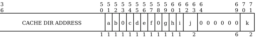
Cache Memory Addressing...343
Cache Memory Control...345
Enabling and Disabling Cache Memory...345
Cache Memory Control in Segment Descriptor Words...345
Loading the Cache Memory...346
Clearing the Cache Memory...346
General Clear...346
Selective Clear...346
Dumping the Cache Memory...347
Appendix A: Operation Code Map...348
Appendix B: Alphabetic Operation Code List...351
EIS Micro Operations...357
Appendix C: Address Modifiers...358
SECTION 1: INTRODUCTION
The processor described in this reference manual is a hardware module designed for use with Multics. The many distinctive features and functions of Multics are enhanced by the powerful hardware features of the processor. The addressing features, in particular, are designed to permit the Multics software to compute relative and absolute addresses, locate data and programs in the Multics virtual memory, and retrieve such data and programs as necessary.
MULTICS PROCESSOR FEATURES
The Multics processor contains the following general features:
1. Storage protection to place access restrictions on specified segments.
2. Capability to interrupt program execution in response to an external signal (e.g., I/O termination) at the end of any even/odd instruction pair (midinstruction interrupts are permitted for some instructions), to save processor status, and to restore the status at a later time without loss of continuity of the program.
3. Capability to fetch instruction pairs and to buffer two instructions (up to four instructions, depending on certain main memory overlap conditions) including the one currently in execution.
4. Overlapping instruction execution, address preparation, and instruction fetch. While an instruction is being executed, address preparation for the next operand (or even the operand following it) or the next instruction pair is taking place. The operations unit can be executing instruction N, instruction N+1 can be buffered in the operations unit (with its operand buffered in a main memory port), and the control unit can be executing instructions N+2 or N+3 (if such execution does not involve the main memory port or registers of instructions N or N+1) or preparing the address to fetch instructions N+4 and N+5. This includes the capability to detect store instructions that alter the contents of buffered instructions and the ability to delay preprocessing of an address using register modification if the instruction currently in execution changes the register to be used in that modification.
5. Interlacing capability to direct main memory accesses to interlaced system controller modules.
6. Intermediate storage of address and control information in high-speed registers addressable by content (associative memory).
7. Intermediate storage of base address and control information in pointer registers that are loaded by the executing program.
8. Absolute address computation at execution time.
9. Ability to hold recently referenced operands and instructions in a high-speed look-aside memory (cache option).
Segmentation and Paging
own origin that can be addressed as location zero. The size of each segment varies without affecting the addressing of the other segments. Each segment can be addressed like a conventional main memory image starting at location zero. Maximum segment size is 262,144 words.
When viewed from the processor, main memory consists of blocks or page frames, each of which has a length of "page-size" words. The page size used by Multics is 1024 words. Each frame begins at an absolute address which is zero modulo the page size. Any page of a segment can be placed in any available main memory frame. These pages may be addressed as if they were contiguous, even though they may be in widely scattered absolute locations. Only currently referenced pages need be in main memory. A segment need not be paged, in which case the complete segment is located in contiguous words of main memory. In Multics, all user segments are paged. See Section 5 for additional discussion.
Address Modification and Address Appending
Before each main memory access, two major phases of address preparation take place: 1. Address modification by register or indirect word content, if specified by the
instruction word or indirect word.
2. Address appending, in which a virtual memory address is translated into an absolute address to access main memory.
Although the above two types of modification are combined in most operations, they are described separately in Sections 5 and 6. The address modification procedure can go on indefinitely, with one type of modification leading to repetitions of the same type or to other types of modification prior to a main memory access for an operand.
Faults and Interrupts
The processor detects certain illegal instruction usages, faulty communication with the main memory, programmed faults, certain external events, and arithmetic faults. Many of the processor fault conditions are deliberately or inadvertently caused by the software and do not necessarily involve error conditions. The processor communicates with the other system modules (I/O multiplexers, bulk store controllers, and other processors) by setting and answering external interrupts. When a fault or interrupt is recognized, a "trap" results. The trap causes the forced execution of a pair of instructions in a main memory location, unique to the fault or interrupt, known as the fault or interrupt vector. The first of the forced instructions may cause safe storage of the processor status. The second instruction in a fault vector should be some form of transfer, or the faulting program will be resumed at the point of interruption. Faults and interrupts are described in Section 7.
Interrupts and certain low-priority faults are recognized only at specific times during the execution of an instruction pair. If, at these times, bit 28 in the instruction word is set ON, the trap is inhibited and program execution continues. The interrupt or fault signal is saved for future recognition and is reset only when the trap occurs.
PROCESSOR MODES OF OPERATION
Instruction Execution Modes
Normal Mode
Most instructions can be executed in the normal mode. Certain instructions, classed as privileged, cannot be executed in normal mode. These are identified in the individual instruction descriptions. An attempt to execute privileged instructions while in the normal mode results in an illegal procedure fault. The processor executes instructions in normal mode only if it is forming addresses in append mode and the segment descriptor word (SDW) for the executing segment specifies a nonprivileged procedure.
Privileged Mode
In privileged mode, all instructions can be executed. The processor executes instructions in privileged mode when forming addresses in absolute mode or when forming addresses in append mode and the segment descriptor word (SDW) for the segment in execution specifies a privileged procedure and the execution ring is equal to zero. See Sections 5 and 7 for additional discussion.
Addressing Modes
Absolute Mode
In absolute mode, the final computed address is treated as the absolute main memory address unless the appending hardware mechanism is invoked for a particular main memory reference. During instruction fetches, the procedure pointer register is ignored. The processor enters absolute mode when it is initialized or immediately after a fault or interrupt. It remains in absolute mode until it executes a transfer instruction whose operand is obtained via explicit use of the appending hardware mechanism.
The appending hardware mechanism may be invoked for an instruction by setting bit 29 of the instruction word ON to cause a reference to a properly loaded pointer register or by the use of indirect-to-segment (its) or indirect-to-pointer (itp) modification in an indirect word.
Append Mode
The append mode is the most commonly used main memory addressing mode. In append mode the final computed address is either combined with the procedure pointer register, or it is combined with one of the eight pointer registers. If bit 29 of the instruction word contains a 0, then the procedure pointer register is selected; otherwise, the pointer register given by bits 0-2 of the instruction word is selected.
BAR Mode
In BAR mode, the base address register (BAR) is used. The BAR contains an address bound and a base address. All computed addresses are relocated by adding the base address. The relocated address is combined with the procedure pointer register to form the virtual memory address. A program is kept within certain limits by subtracting the unrelocated computed address from the address bound. If the result is zero or negative, the relocated address is out of range, and a store fault occurs.
PROCESSOR UNIT FUNCTIONS
Appending Unit
Controls data input/output to main memory Performs main memory selection and interlace Does address appending
Controls fault recognition Interfaces with cache
Associative Memory Assembly
This assembly consists of sixteen 51-bit page table word associative memory (PTWAM) registers and sixteen 108-bit segment descriptor word associative memory (SDWAM) registers. These registers are used to hold pointers to most recently used segments (SDWs) and pages (PTWs). This unit reduces the need for possible multiple main memory accesses before obtaining an absolute main memory address of an operand or instruction.
Control Unit
Performs address modification
Controls mode of operation (privileged, normal, etc.) Performs interrupt recognition
Decodes instruction words and indirect words Performs timer register loading and decrementing
Operation Unit
Does fixed- and floating-binary arithmetic Does shifting and Boolean operations
Decimal Unit
Does decimal arithmetic
SECTION 2: DATA REPRESENTATION
INFORMATION ORGANIZATION
The processor, like the rest of the Multics system, is organized to deal with information in basic units of 36-bit words. Other units of 4-, 6-, 9-bit characters or bytes, 18-bit half words, and 72-bit word pairs can be manipulated within the processor by use of the instruction set. These bit groupings are used by the hardware and software to represent a variety of forms of coded data. Certain processor functions appear to manipulate larger units of 144, 288, 576, and 1152 bits, but these functions are performed by means of repeated use of 72-bit word pairs. All information is transmitted, stored, and processed as strings of binary bits. The data values are derived when the bit strings are interpreted according to the various formats discussed in this section.
POSITION NUMBERING
The numbering of bit positions, character and byte positions, and words increases from 0 in the direction of conventional reading and writing: from the most significant to the least significant digit of a number, and from left to right in conventional alphanumeric text.
Graphic presentations in this manual show registers and data with position numbers increasing from left to right.
NUMBER SYSTEM
The binary arithmetic functions of the processor are implemented in the twos complement, binary number system. One of the primary properties of this number system is that a field (or register) having width n bits may be interpreted in two different ways; the logical case and the arithmetic or algebraic case.
In the logical case, the number is unsigned, positive, and lies in the range [0,2n-1] where n is the size of the register or the length of the field. The results of arithmetic operations on numbers for this case are interpreted as modulo 2n numbers. Overflow is not defined for this case since the range of the field or register cannot be exceeded. The numbers 0 and 2n-1 are consecutive (not separated) in the set of numbers defined for the field or register.
In the arithmetic case, the number is signed and lies in the range [-2(n-1),2(n-1)-1]. Overflow is defined for this case since the range can be exceeded in either direction (positive or negative). The left-hand-most bit of the field or register (bit 0) serves as the sign bit and does not contribute to the magnitude of the number.
The main advantage of this implementation is that the hardware arithmetic algorithms for the two cases are identical; the only distinction lying in the interpretation of the results by the user. Instruction set features are provided for performing binary arithmetic with overflow disabled (the so-called logical instructions) and for comparing numbers in either sense.
Subtraction is performed by adding the twos complement of the subtrahend to the minuend. (Note that when the subtrahend is zero the algorithm for forming the twos complement is still carried out, but, since the twos complement of zero is zero, the result is correct.)
Another important feature of the twos complement number system (with respect to comparison of numeric values) is that the no borrow condition in true subtraction is identical to the carry condition in true addition and vice versa.
right of the least significant bit position, that is, to the right of the right-hand-most bit of the field or register, and fraction means that the position of the binary point is assumed to the left of the most significant bit position, that is, between bit 0 and bit 1 of the field or register (recall that bit 0 is the sign bit).
INFORMATION FORMATS
The figures that follow show the unstructured formats (templates) for the various information units defined for the processor. Data transfer between the processor and main memory is word oriented; a 36-bit machine word is transferred for single-precision operands and subfields of machine words, and a 72-bit word pair is transferred for all other cases (multiword operands, instruction fetches, bit- and character-string operands, etc.). The information unit to be used and the data transfer mode are determined by the processor according to the function to be performed.
The 36-bit unstructured machine word shown in Figure 2-1 is the minimum addressable information unit in main memory. Its location is uniquely determined by its main memory address, Y. All other information units are defined relative to the 36-bit machine word.
Figure 2-1. Unstructured Machine Word Format
Two consecutive machine words as shown in Figure 2-2, the first having an even main memory address, form a 72-bit word pair. In 72-bit word pair data transfer mode, the word pair is uniquely located by the main memory address of either of its constituent 36-bit machine words. Thus, if Y is even, the word pair at (Y,Y+1) is selected. If Y is odd, the word pair at (Y-1,Y) is selected. The term Y-pair is used when referring to such a word pair.
Figure 2-2. Unstructured Word Pair Format
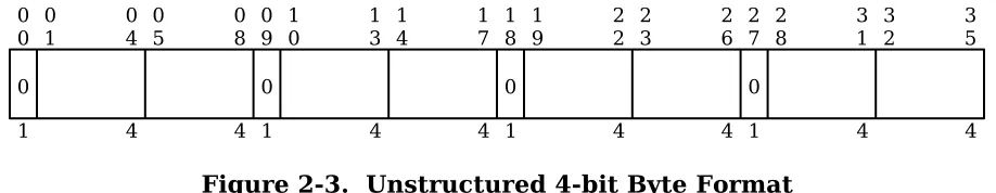
[image:13.612.77.536.617.706.2]Four-bit bytes are mapped onto 36-bit machine words as shown in Figure 2-3. The 0 bits at bit positions 0, 9, 18, and 27 are forced to be 0 by the processor on data transfers to main memory and are ignored on data transfers from main memory.
Figure 2-3. Unstructured 4-bit Byte Format
Six-bit characters are mapped onto 36-bit machine words as shown in Figure 2-4.
0 0 36 3 5 0
0 35
36 3
6 71
36
Even word Odd word
0 0
0
1 0
1 04
4 0
5 08
4 0 9 0 1 1
0 13
4 1
4 17
4 1 8 0 1 1
9 22
4 2
3 26
4 2 7 0 1 2
8 31
4 3
2 35
Figure 2-4. Unstructured 6-bit Character Format
Nine-bit bytes are mapped onto 36-bit machine words as shown in Figure 2-5.
Figure 2-5. Unstructured 9-bit Byte Format
Eighteen-bit half words are mapped onto 36-bit machine words as shown in Figure 2-6.
Figure 2-6. Unstructured 18-bit Half Word Format
DATA PARITY
Odd parity on each 36-bit machine word transferred to main memory is generated as it leaves the processor, is verified at several points along the transmission path, and is held in main memory either as an extra bit in the case of magnetic core memory or as part of the error detecting and correcting (EDAC) code in the case of magnetic oxide semiconductor (MOS) memory. If an incorrect parity is detected at any of the various parity check points, the main memory returns an illegal action signal and a code appropriate to the check point.
On data transfers from main memory, the parity information is retrieved and transmitted with the data information. The same verification checks are made and illegal action signalled for errors. The processor makes a final parity check as the data enters the processor.
Any detected parity error causes the processor parity indicator to be set ON and (if enabled) a parity fault occurs.
REPRESENTATION OF DATA
Data is defined by imposing an operand structure on the information units just described. Data is represented in two forms: numeric or alphanumeric. The form is determined by the processor according to the function to be performed.
In the definitions below, ai is the value of the bit in the ith bit position, either 0 or 1.
0
0 05
6 0
6 11
6 1
2 17
6 1
8 23
6 2
4 29
6 3
0 35
6
0
0 08
9 0
9 17
9 1
8 26
9 2
7 35
9
Upper half Lower half
0
0 17
18 1
8 35
Numeric Data
Numeric data is represented in three modes: fixed-point binary, floating-point binary, and decimal. The mode is determined by the processor according to the function being performed.
Fixed-point Binary Data
Fixed-point Binary Integers
Fixed-point binary integer data is defined by imposing either of the bit position value expressions shown below on an information unit of n bits.
Logical value:
a0×2(n-1) + a1×2(n-2) + ... + ai×2(n-i-l) + ... + an-1
Arithmetic value:
-a0×2(n-l) + a1×2(n-2) + ... + ai×2(n-i-l) + ... + an-l
The following fixed-point binary integer data items are defined (also see Table 2-1 for values):
Operand size (bits) Operand name
6 6-bit character operand 9 9-bit byte operand 18 Half word operand 36 Single-precision operand 72 Double-precision operand
Note that a 4-bit operand is not defined. This data item is defined only for decimal data. (See discussion of decimal data later in this section).
The proper operand and its position with respect to a 36-bit machine word are determined by the processor during preparation of the main memory address for the operand. If the data width of the operand selected is smaller than the register involved, the operand is high- or low-order zero filled as necessary.
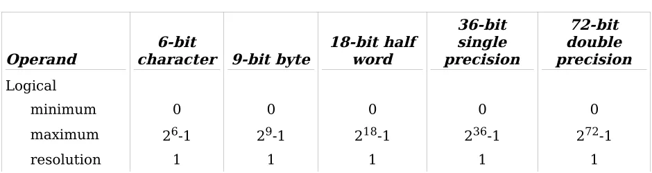
[image:15.612.71.541.617.742.2]The values in Table 2-1 are given in terms of the operand sizes. The value an operand contributes to a larger field or register depends on the alignment of the operand with respect to the field or register.
Table 2-1. Fixed-Point Binary Integer Values
Operand character 9-bit byte6-bit 18-bit half word
36-bit single precision
72-bit double precision
Logical
minimum 0 0 0 0 0
maximum 26-1 29-1 218-1 236-1 272-1
Operand character 9-bit byte6-bit 18-bit half word
36-bit single precision
72-bit double precision
Arithmetic
minimum 0 0 0 0 0
maxima
negative -25 -28 -217 -235 -271
positive 25-1 28-1 217-1 235-1 271-1
resolution 1 1 1 1 1
Fixed-point Binary Fractions
Fixed-point binary fraction data is defined by imposing the bit position value expression below on an information unit of n bits.
Arithmetic value:
-a0 + a1×2-1 + a2×2-2 + ... + ai×2-i + ... + an-l×2-(n-l)
Note that logical values are not defined for fixed-point binary fraction data.
The following fixed-point binary fraction data items are defined (also see Table 2-2 for values):
Operand size (bits) Operand name
6 6-bit character operand 9 9-bit byte operand 18 Half word operand 36 Single-precision operand 72 Double-precision operand
Note that a 4-bit operand is not defined. This data item is defined only for decimal data. (See discussion of decimal data later in this section.) Fixed-point binary fraction operands are used by the Divide Fraction (dvf) and Multiply Fraction (mpf) instructions only.
The proper operand and its position with respect to a 36-bit machine word are determined by the processor during preparation of the main memory address for the operand. If the data width of the operand selected is smaller than the register involved, the operand is high- or low-order zero filled as necessary.
Table 2-2. Fixed-Point Binary Fraction Values
Operand character 9-bit byte6-bit 18-bit half word
36-bit single precision
72-bit double precision
Arithmetic
minimum 0 0 0 0 0
maxima
negative -1.0 -1.0 -1.0 -1.0 -1.0
positive 1.0-2-5 1.0-2-8 1.0-2-17 1.0-2-35 1.0-2-71
resolution 2-5 2-8 2-17 2-35 2-71
Floating-point Binary Data
A floating-point binary number is expressed as:
Z = M × 2E where:
M is a fixed-point binary fraction; the mantissa E is a fixed-point binary integer; the exponent
A floating-point binary number is defined by partitioning an information unit of n bits into two pieces; an 8-bit fixed-point binary integer exponent and an (n-8)-bit fixed-point binary fraction mantissa.
The following floating-point data items are defined.
Operand size (bits) Operand name 18 Half word operand 36 Single-precision operand 72 Double-precision operand
For clarity, the formats of these operands are shown in Figure 2-7 through Figure 2-9. In the figures, the fields labeled S hold sign bits associated with the exponent, E, and the mantissa, M.
The floating-point binary operands are used only by the floating-point binary arithmetic instructions (see Section 4). The 18-bit half word operand has meaning only when used in conjunction with the direct upper (du) address modification (see Section 6 for a discussion of address modification).
Figure 2-7. Eighteen-bit Half Word Floating-Point Binary Operand Format 0
0
S
1 0 1
E
0 7
7 0 8
S
1 0 9
M
1 7
Figure 2-8. Single-Precision Floating-Point Binary Operand Format
Figure 2-9. Double-Precision Floating-Point Binary Operand Format
The proper operand is selected by the processor during preparation of the main memory address for the operand.
Overlength Registers
The register is used to hold the mantissa of all floating-point binary numbers. The AQ-register is said to be overlength with respect to the operands since it has more bits than are provided by the operands. Operands are low-order zero filled when loaded and low-order truncated (or rounded, depending on the instruction) when stored. Thus, the result of all floating-point instructions has more bits of precision in the AQ-register than may be stored.
Users are cautioned that calculations involving floating-point operands may suffer from propagation of truncation errors even if the computation algorithms are designed to hold mantissas in the AQ-register as long as possible. It is possible to retain full AQ-register precision of intermediate results if they are saved with the Store AQ (staq) and Store Exponent (ste) instructions but such saved data are not usable as a floating-point operand.
Normalized Numbers
A floating-point binary number is said to be normalized if the relation -0.5 > M > -1 or 0.5 ≤ M < 1 or [M=0 and E=-128]
is satisfied. This is a result of using a 2's complement mantissa. Bits 8 and 9 are different unless the number is zero. The presence of unnormalized numbers in any finite mantissa arithmetic can only degrade the accuracy of results. For example, in an arithmetic allowing only two digits in the mantissa, the number 0.005×10² has the value zero instead of the value one-half.
Normalization is a process of shifting the mantissa and adjusting the exponent until the relation above is satisfied. Normalization may be used to recover some or all of the extra bits of the overlength AQ-register after a floating-point operation.
There are cases where the limits of the registers force the use of unnormalized numbers. For example, in an arithmetic allowing three digits of mantissa and one digit of exponent, the calculation 0.3×10⁻¹⁰ - 0.1×10⁻¹¹ (the normalized case) may not be made, but 0.03×10⁻⁹ – 0.001×10-9 = 0.029×10⁻⁹ (the unnormalized case) is a valid result.
Some examples of normalized and unnormalized floating-point binary numbers are:
Unnormalized positive binary 0.00011010 × 27
0 0
S
1 0 1
E
0 7
7 0 8
S
1 0 9
M
3 5
27
0 0
S
1 0 1
E
0 7
7 0 8
S
1 0 9
M
7 1
Same number normalized 0.11010000 × 24
Unnormalized negative binary 1.11010111 × 2-4
Same number normalized 1.01011100 × 2-6
The minimum normalized nonzero floating-point binary number is 2-128 in all cases. Table 2-3 gives the values for the floating-point binary operands.
Table 2-3. Floating-Point Binary Operand Values
Operand 18-bit half word 36-bit single precision 72-bit double precision
Unnormalized
minimum 0 (a) 0 (a) 0 (a)
maxima
negative -1.0×2127 -1.0×2127 -1.0×2127 positive (1-2-9)×2127 (1-2-27)×2127 (1-2-63)×2127
resolution 1:9 (b) 1:27 (b) 1:63 (b)
(a)There is no unique representation for the value zero in floating-point binary numbers; any number with mantissa zero has the value zero. However, the processor treats a zero mantissa as a special case in order to preserve precision in later calculations with a zero intermediate result. Whenever the processor detects a zero mantissa as the result of a floating-point binary operation, the AQ-register is cleared to zeros and the E register is set to -128. This representation is known as a floating-point normalized zero. The unnormalized zero (any zero mantissa) will be handled correctly if encountered in an operand but precision may be lost. For example, A×10-14 + 0×1038 will not produce desired results since all the precision of A will be lost when it is aligned to match the 1038 exponent of the 0.
(b)A value cannot be given for resolution in these cases since such a value depends on the value of the exponent, E. The notation used, l:m, indicates resolution to 1 bit in a field of m. Thus, the following general statement on resolution may be made:
The resolution of a floating-point binary operand with mantissa length m and exponent value E is 2(E-m).
Decimal Data
Decimal numbers are expressed in the following forms: Fixed-point, no sign MMMMMM.
Fixed-point, leading sign ±MMMMMM. Fixed-point, trailing sign MMMMMM.±
Floating-point ±MMMMMM.×10E
A decimal number is defined by imposing any of the byte position value expressions below on a 4- or 9-bit byte information unit of length n bytes.
Fixed-point, no sign:
c0×10(n-1) + c1×10(n-2) + ... + c(n-1)
Fixed-point, leading sign:
[sign=c0] c1×10(n-2) + c2×10(n-3) + ... + c(n-1)
Fixed-point, trailing sign:
c0×10(n-2) + c1×10(n-3) + ... + c(n-2) [sign=c(n-1)]
Floating-point:
[sign=c0] c1×10(n-3) + c2×10(n-4) + ... + c(n-3) [exponent=8 bits]
where:
ci is the decimal value of the byte in the ith byte position.
[sign=ci] indicates that ci is interpreted as a sign byte.
[exponent=8 bits] indicates that the exponent value is taken from the last 8 bits of the string. If the data is in 9-bit bytes, the exponent is bits 1-8 of c(n-1). If the data is in 4-bit bytes, the exponent is the binary value of the concatenation of c(n-2) and c(n-1).
The decimal number as described above is the only decimal data item defined. It may begin on any legal byte boundary (without regard to word boundaries) and has a maximum extent of 63 bytes.
The processor handles decimal data as 4-bit bytes internally. Thus, 9-bit bytes are high-order truncated as they are transferred from main memory and high-high-order filled as they are transferred to main memory. The fill pattern is "00011"b for digit bytes and "00010" for sign bytes. The floating-point exponent is a special case and is treated as a fixed-point binary integer.
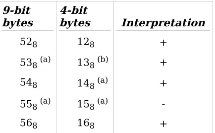
[image:20.612.199.416.610.744.2]The processor performs validity checking on decimal data. Only the byte values [0,11]8 are legal in digit positions and only the byte values [12,17]8 are legal in sign positions. Detection of an illegal byte value causes an illegal procedure fault. The interpretation of decimal sign bytes is shown in Table 2-4.
Table 2-4. Decimal Sign Character Interpretation
9-bit
bytes 4-bit bytes Interpretation
528 128 +
538 (a) 138 (b) +
548 148 (a) +
558 (a) 158 (a)
9-bit
bytes 4-bit bytes Interpretation
578 178 +
(a)This value is used as the default sign byte for storage of results. The presence of other values will yield correct results according to the interpretation.
(b)An optional control bit in the EIS decimal arithmetic instructions (see Section 4) allows the selection of 138 for the plus sign byte for storage of results in 4-bit data mode.
Decimal Data Values
The operand descriptors for decimal data operands have a 6-bit fixed-point binary integer field for specification of a scaling factor (SF). This scaling factor has the same effect as the value of E in floating-point decimal operands; a negative value moves the assumed decimal point to the left; a positive value, to the right. The use of the scaling factor extends the range and resolution of decimal data operands. The range of the scaling factor is [-32,31]10. See Table 2-5 for decimal data operand values.
Table 2-5. Decimal Data Values
Operand Fixed-point unsigned Fixed-point signed Floating-point 9 bit Floating-point 4 bit
Arithmetic
minimum 0 0 (a) 0 (a) 0 (a)
maximum (1063-1)×1031 ±(1062-1)×1031 ±(1061-1)×10158 ±(1060-1)×10158 resolution 1:SF (b) 1:SF (b) 1:E (c) 1:E (c)
(a)As in floating-point binary arithmetic, there is no unique representation of the value zero except in the case of fixed-point, unsigned data. Therefore, the processor detects a zero result and forces a value of +0. for fixed-point, signed data and +0.×10127 for floating-point data. Again, as in floating-point binary arithmetic, other representations of the value zero will be handled correctly except for possible loss of precision during operand alignment.
(b)A value cannot be given for resolution in these cases since such a value depends on the value of the scaling factor, SF. The notation used, 1:SF, indicates resolution to 1 part in 10(SF). Thus, the following general statement on resolution may be made:
The resolution of a fixed-point decimal operand with scaling factor SF is 10SF.
(c)A value cannot be given for resolution in these cases since such a value depends on the value of the exponent, E. The notation used, 1:E, indicates resolution to 1 part in 10(E). Thus, the following general statement on resolution may be made:
The resolution of a floating-point decimal operand with exponent E is 10(E). The scaling factor is ignored by the hardware.
Alphanumeric Data
Character String Data
Character string data is defined by imposing the character position structure below on a 4-bit, 6-4-bit, or 9-bit information unit of length n bytes or characters.
c0 || c1 || ... || c(n-1)
where:
ci is the character in the ith character position.
|| indicates the concatenation operation.
The character string described above is the only character string data item defined. It may begin on any legal character boundary (without regard to word boundaries) and has a maximum extent as shown in Table 2-6.
Table 2-6. Character String Data Length Limits
Character size Length limit
9-bit 1048576
6-bit 1572864
4-bit 2097152
No interpretation of the characters is made except as specified for the instruction being executed (see Section 4).
Bit String Data
Bit string data is defined by imposing the bit position structure below on a bit information unit of length n bits.
b0 || b1 || ... || b(n-1)
where:
bi is the value of the bit in the ith position.
|| indicates the concatenation operation.
SECTION 3: PROGRAM ACCESSIBLE REGISTERS
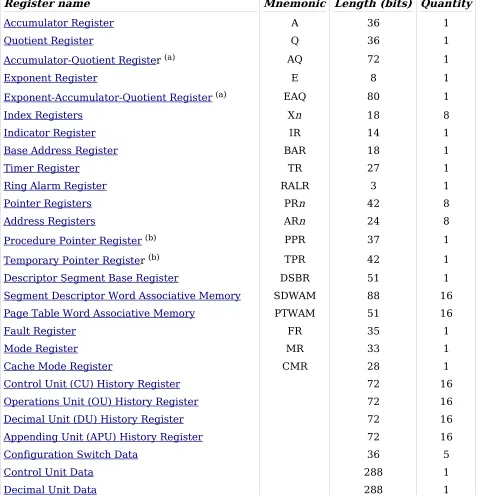
[image:23.612.68.545.202.697.2]A processor register is a hardware assembly that holds information for use in some specified way. An accessible register is a register whose contents are available to the user for his purposes. Some accessible registers are explicitly addressed by particular instructions, some are implicitly referenced during the course of execution of instructions, and some are used in both ways. The accessible registers are listed in Table 3-1. See Section 4 for a discussion of each instruction to determine the way in which the registers are used.
Table 3-1. Processor Registers
Register name Mnemonic Length (bits) Quantity
Accumulator Register A 36 1
Quotient Register Q 36 1
Accumulator-Quotient Register (a) AQ 72 1
Exponent Register E 8 1
Exponent-Accumulator-Quotient Register(a) EAQ 80 1
Index Registers Xn 18 8
Indicator Register IR 14 1
Base Address Register BAR 18 1
Timer Register TR 27 1
Ring Alarm Register RALR 3 1
Pointer Registers PRn 42 8
Address Registers ARn 24 8
Procedure Pointer Register (b) PPR 37 1
Temporary Pointer Register (b) TPR 42 1
Descriptor Segment Base Register DSBR 51 1
Segment Descriptor Word Associative Memory SDWAM 88 16
Page Table Word Associative Memory PTWAM 51 16
Fault Register FR 35 1
Mode Register MR 33 1
Cache Mode Register CMR 28 1
Control Unit (CU) History Register 72 16
Operations Unit (OU) History Register 72 16
Decimal Unit (DU) History Register 72 16
Appending Unit (APU) History Register 72 16
Configuration Switch Data 36 5
Control Unit Data 288 1
Decimal Unit Data 288 1
(b)This register is not explicitly addressable, but is included because of its vital role in instruction and operand address preparation.
In the descriptions that follow, the diagrams given for register formats do not imply that a physical assembly possessing the pictured bit pattern exists. The diagram is a graphic representation of the form of the register data as it appears in main memory when the register contents are stored or how data bits must be assembled for loading into the register.
If the diagrams contain the characters "x" or "0", the values of the bits in the positions shown are irrelevant to the register. Bits pictured as "x" are not changed when the register is stored. Bits pictured as "0" are set to 0 when the register is stored. Neither "x" bits or "0" bits are loaded into the register.
ACCUMULATOR REGISTER (A)
Format: - 36 bits
Figure 3-1. Accumulator Register (A) Format
Description:
A 36-bit physical register located in the operations unit.
Function:
In fixed-point binary instructions, holds operands and results.
In floating-point binary instructions, holds the most significant part of the mantissa. In shifting instructions, holds original data and shifted results.
In address preparation, may hold two logically independent word offsets, upper and A-lower, or an extended range bit- or character-string length.
QUOTIENT REGISTER (Q)
Format: - 36 bits
Figure 3-2. Quotient Register (Q) Format
Description:
A 36-bit physical register located in the operations unit.
A-Upper A-Lower
0
0 17
18 1
8 35
18
Q-Upper Q-Lower
0
0 17
18 1
8 35
Function:
In fixed-point binary instructions, holds operands and results.
In floating-point binary instructions, holds the least significant part of the mantissa. In shifting instructions, holds original data and shifted results.
In address preparation, may hold two logically independent word offsets, upper and Q-lower, or an extended range bit- or character-string length.
ACCUMULATOR-QUOTIENT REGISTER (AQ)
Format: - 72 bits
Figure 3-3. Accumulator-Quotient Register (AQ) Format
Description:
A combination of the accumulator (A) and quotient (Q) registers.
Function:
In fixed-point binary instructions, holds double-precision operands and results. In floating-point binary instructions, holds the mantissa.
In shifting instructions, holds original data and shifted results.
EXPONENT REGISTER (E)
Format: - 8 bits
Figure 3-4. Exponent Register (E) Format
Description:
An 8-bit physical register located in the operations unit.
Function:
In floating-point binary instructions, holds the exponent.
Even word Odd word
A Q
0
0 35
36 3
6 71
36
0 0
8 0 7 08
0 0 0 0 0 0 0 0 0 0 0 0 0 0 0 0 0 0 0 0 0 0 0 0 0 0 0 3 5
0
EXPONENT-ACCUMULATOR-QUOTIENT REGISTER (EAQ)
Format: - 80 bits
Figure 3-5. Exponent-Accumulator-Quotient Register (EAQ) Format
Description:
A combination of the exponent (E), accumulator (A), and quotient (Q) registers. Although the combined register has a total of 80 bits, only 72 are involved in transfers to and from main memory. The 8 low-order bits are discarded on store and zero-filled on load.
Function:
In floating-point binary instructions, holds operands and results.
INDEX REGISTERS (X
n
)
Format: - 18 bits each
Figure 3-6. Index Register (X
n
) FormatDescription:
Eight 18-bit physical registers in the operations unit numbered 0 through 7. Index register data may occupy the position of either an upper or lower 18-bit half-word operand (see
Section 2).
Function:
In fixed-point binary instructions, hold half-word operands and results.
In address preparation, hold word offsets or extended range bit- or character-string lengths.
0 0
8 0
7 08 71
64
exponent mantissa
0
0 17
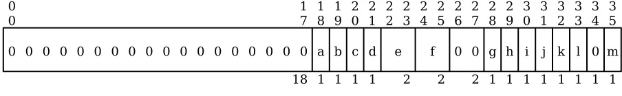
INDICATOR REGISTER (IR)
Format: - 14 bits
Figure 3-7. Indicator Register (IR) Format
Description:
An assemblage of 15 indicator flags from various units of the processor. The data occupies the position of a lower 18-bit half word operand (see Section 2). When interpreted as data, a bit value of 1 corresponds to the ON state of the indicator, a bit value of 0 corresponds to the OFF state.
Function:
The functions of the individual indicator bits are given below. An "x" in the column headed "L" indicates that the state of the indicator is not affected by instructions that load the IR.
key L Indicator name Action
a Zero This indicator is set ON whenever the output of the main binary adder consists entirely of zero bits for binary or shifting instructions or the output of the decimal adder consists entirely of zero digits for decimal instructions; otherwise, it is set OFF. b Negative This indicator is set ON whenever the output of bit 0 of the main
binary adder has value 1 for binary or shifting instructions or the sign character of the result of a decimal instruction is the negative sign character; otherwise, it is set OFF.
c Carry This indicator is set ON for any of the following conditions; otherwise, it is set OFF.
(1) If a bit propagates leftward out of bit 0 of the main binary adder for any binary or shifting instruction.
(2) If | value1 | <= | value2 | for a decimal numeric comparison instruction.
(3) If char1 <= char2 for a decimal alphanumeric compare instruction.
d Overflow This indicator is set ON if the arithmetic range of a register is exceeded in a fixed-point binary instruction or if the target string of a decimal numeric instruction is too small to hold the integer part of the result. It remains ON until reset by the Transfer On Overflow (tov) instruction or is reset by some other instruction that loads the IR. The event that sets this indicator ON may also cause an overflow fault. (See overflow mask indicator below.)
0 0
key L Indicator name Action e Exponent
overflow This indicator is set ON if the exponent of the result of a floating-point binary or decimal numeric instruction is greater than +127. It remains ON until reset by the Transfer On Exponent Overflow (teo) instruction or is reset by some other instruction that loads the IR. The event that sets this indicator ON may also cause an overflow fault. (See overflow mask indicator below.)
f Exponent
underflow This indicator is set ON if the exponent of the result of a floating-point binary or decimal numeric instruction is less than -128. It remains ON until reset by the Transfer On Exponent Underflow (teu) instruction or is reset by some other instruction that loads the IR. The event that sets this indicator ON may also cause an overflow fault. (See overflow mask indicator below.) g Overflow mask This indicator is set ON or OFF only by the instructions that load
the IR. When set ON, the IR inhibits the generation of the fault for those events that normally cause an overflow fault. If the overflow mask indicator is set OFF after occurrence of an overflow event, an overflow fault does not occur even though the indicator for that event is still set ON. The state of the overflow mask indicator does not affect the setting, testing, or storing of any other indicator.
h Tally runout This indicator is set OFF at initialization of any tallying operation, that is, any repeat instruction or any indirect then tally address modification. It is then set ON for any of the following conditions:
(1) If any repeat instruction terminates because of tally exhaust.
(2) If a Repeat Link (rpl) instruction terminates because of a zero link address.
(3) If a tally exhaust is detected for an indirect then tally modifier. The instruction is executed whether or not tally exhaust occurs.
(4) If an EIS string scanning instruction reaches the end of the string without finding a match condition.
i Parity error This indicator is set ON whenever a system controller signals illegal action with a parity error code or the processor detects an internal parity error condition. The indicator is set OFF only by instructions that load the IR.
key L Indicator name Action
k x Not BAR mode This indicator is set OFF (placing the processor in BAR mode) only by execution of the Transfer and Set Slave (tss) instruction or by the operand data of the Restore Control Unit (rcu) instruction and is changed only when the processor is in privileged or absolute mode. It is set ON (taking the processor out of BAR node) by the execution of any transfer instruction other than tss during a fault or interrupt trap. (See Section 7.) If a fault or interrupt trap occurs while in BAR node and the IR is stored before any transfer occurs, then a Return (ret) or Restore Control Unit (rcu) instruction that reloads the stored data will return the processor to BAR mode.
l Truncation This indicator is set ON whenever the target string of a decimal numeric instruction is too small to hold all the digits of the result or the target string of an alphanumeric instruction is too small to hold all the bits or characters to be stored. (Also see the overflow indicator for decimal numeric instructions.) The event that sets this indicator ON may also cause an overflow fault. (See overflow mask indicator above.)
m Mid instruction
interrupt fault This indicator is set OFF at the start of execution of each instruction and is set ON by the events described below. The indicator has meaning only when determining the proper restart sequence for the interrupted instruction. This indicator can be set on:
(1) By any fault during execution of an EIS instruction; however, the state is safe-stored in the Control Unit Data only for access violation and directed faults.
(2) By an interrupt signal during execution of those EIS instructions that allow very long operand strings.
(3) If the processor is in absolute or privileged mode, by the execution of a Load Indicator Register (ldi), Return (ret), or Restore Control Unit (rcu) instruction with bit 30 set to 1 in the IR data.
n x Absolute mode This indicator is set ON (placing the processor in absolute mode) when the processor is initialized and by execution of an nonappended transfer instruction during a fault or interrupt trap and is set OFF (placing the processor in append mode) by any execution of an appended transfer instruction. If the processor is not in absolute mode when the fault or interrupt occurs and the transfer instruction is Return (ret) or Restore Control Unit (rcu) and the appropriate mode bit is properly set in the IR data, the processor remains in its current mode.
BASE ADDRESS REGISTER (BAR)
Format: - 18 bits
Figure 3-8. Base Address Register (BAR) Format
Description:
An 18-bit physical register in the control unit.
Function:
The Base Address Register provides automatic hardware Address relocation and Address range limitation when the processor is in BAR mode.
BAR.BASE Contains the 9 high-order bits of an 18-bit address relocation constant. The low-order bits are generated as zeros.
BAR.BOUND Contains the 9 high-order bits of the unrelocated address limit. The low-order bits are generated as zeros. An attempt to access main memory beyond this limit causes a store fault, out of bounds. A value of 0 is truly 0, indicating a null memory range.
TIMER REGISTER (TR)
Format: - 27 bits
Figure 3-9. Timer Register (TR) Format
Description:
A 27-bit settable, free-running clock in the control unit. The value decrements at a rate of 512 kHz. Its range is 1.953125 microseconds to approximately 4.37 minutes.
Function:
The TR may be loaded with any convenient value with the privileged Load Timer (ldt) instruction. When the value next passes through zero, a timer runout fault is signalled. If the processor is in normal or BAR mode with interrupts not inhibited or is stopped at an uninhibited Delay Until Interrupt Signal (dis) instruction, the fault occurs immediately. If the processor is in absolute or privileged mode or has interrupts inhibited, the fault is delayed until the processor returns to uninhibited normal or BAR mode or stops at an uninhibited Delay Until Interrupt Signal (dis) instruction.
0
0 08
9 0
9 17
9 1 8
x x x x x x x x x x x x x x x x x 3 5
x
18
BASE BOUND
0
0 26
27 2 7
0 0 0 0 0 0 0 0 3 5
0
RING ALARM REGISTER (RALR)
[image:31.612.63.536.398.625.2]Format: - 3 bits
Figure 3-10. Ring Alarm Register (RALR) Format
Description:
A 3-bit physical register in the appending unit.
Function:
If the RALR contains a value other than zero and the effective ring number (see TPR.TRR
below) is greater than or equal to the contents of the RALR and the instruction for which an absolute main memory address is being prepared is a transfer instruction, an access violation, ring alarm, fault occurs. Operating system software may use this register to detect crossings from inner rings to outer rings.
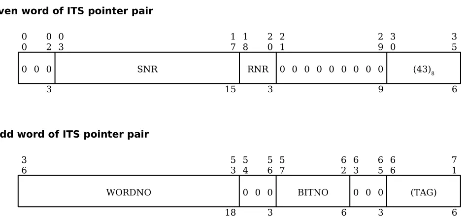
POINTER REGISTERS (PR
n
)
Format: - 42 bits each
Even word of ITS pointer pair
Odd word of ITS pointer pair
0 0
0 0 0 0 0 0 0 0 0 0 0 0 0 0 0 0 0 0 0 0 0 0 0 0 0 0 0 0 0 0 0 0 3 2 0 33 3 3 RALR 3 5 3 15 0 0 0 0 0 2 0 3 0
3 17 18
SNR 2 0 3 2 1
0 0 0 0 0 0 0 0 2 9 0 9 3 0 (43)8 3 5 6 RNR 3
6 53
18 5 4 0 0 5 6 0 3 5
7 62
6 6 3 0 0 6 5 0 3 6
6 71
6 (TAG) BITNO
Data as stored by Store Pointer Register n Packed (sprpn)
Figure 3-11. Pointer Register (PR
n
) FormatDescription:
Eight combinations of physical registers from the appending unit and decimal unit numbered 0 through 7. PRn.RNR, PRn.SNR, and PRn.BITNO are located in the appending unit and PRn.WORDNO is located in the decimal unit. The WORDNO registers also form part of the address registers discussed later in this section.
Function:
The pointer registers hold information relative to the location in main memory of data items that may be external to the segment containing the procedure being executed. The functions of the individual constituent registers are:
Register Function
PRn.SNR The segment number of the segment containing the data item described by the pointer register.
PRn.RNR The final effective ring number value calculated during execution of the instruction that last loaded the PR.
(43)8 This field is not part of the PR but is generated each time the PR is stored as an ITS pair.
PRn.WORDNO The offset in words from the base or origin of the segment to the data item.
PRn.BITNO The number of the bit within PRn.WORDNO that is the first bit of the data item. Data items aligned on word boundaries always have the value 0. Unaligned data items may have any value in the range [1,35].
(TAG) This field is not part of the PR but, in an ITS pointer pair, holds an address modifier for use in address preparation.
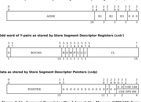
ADDRESS REGISTERS (AR
n
)
Format: - 24 bits each
Data as stored by Store Address Register n (sarn)
Figure 3-12. Address Register (AR
n
) Format 00 05
6 0
6 17
WORDNO
12 1
8 35
18 SNR
BITNO
0
0 17
18 1 8
a 1 9
2 2
0 23
BITNO
4 2 4
0 0 0 0 0 0 0 0 0 0 0 3 5
0
Description:
Eight combinations of physical registers from the decimal unit numbered 0 through 7. The WORDNO registers also form part of the pointer registers discussed earlier in this section.
Function:
The address registers hold information relative to the location in main memory of the next bit, character, or byte of an EIS operand to be processed by an EIS instruction. The functions of the individual constituent registers are:
key Register Function
ARn.WORDNO The offset in words relative to the current addressing base referent (segment origin, BAR.BASE, or absolute 0 depending on addressing mode) to the word containing the next data item element.
a ARn.CHAR The number of the 9-bit byte within ARn.WORDNO containing the first bit of the next data item element.
ARn.BITNO The number of the bit within ARn.CHAR that is the first bit of the next data item element.
NOTE: The reader's attention is directed to the presence of two bit number registers, PRn.BITNO and ARn.BITNO. Because the Multics processor was implemented as an enhancement to an existing design, certain apparent anomalies appear. One of these is the difference in the handling of unaligned data items by the appending unit and decimal unit. The decimal unit handles all unaligned data items with a 9-bit byte number and bit offset within the byte. Conversion from the description given in the EIS operand descriptor is done automatically by the hardware. The appending unit maintains compatibility with the earlier generation Multics processor by handling all unaligned data items with a bit offset from the prior word boundary; again with any necessary conversion done automatically by the hardware. Thus, a pointer register, PRn, may be loaded from an ITS pointer pair having a pure bit offset and modified by one of the EIS address register instructions (a4bd, s9bd, etc.) using character displacement counts. The automatic conversion performed ensures that the pointer register, PRi, and its matching address register, ARi, both describe the same physical bit in main memory. SPECIAL NOTICE: The decimal unit has built-in hardware checks for illegal bit offset values but
the appending unit does not except for a single case for packed pointers. See NOTES for Load Packed Pointers (lprpn) in Section 4.
PROCEDURE POINTER REGISTER (PPR)
Format: - 37 bits
Shown as part of word 0 of control unit data
0 0
PRR 0 2
3 0 3
PSR
1 7
15 1 8
P
1
Shown as part of word 4 of control unit data
Figure 3-13. Procedure Pointer Register (PPR) Format
Description:
A combination of physical registers from the appending unit and the control unit. PPR.PRR, PPR.PSR, and PPR.P are located in the appending unit and PPR.IC is located in the control unit. The PPR is not explicitly addressable but its data is extracted and stored as part of the data stored with the Store Control Unit (scu) and Store Control Double (stcd) instructions. It is loaded from the control unit data with the Restore Control Unit (rcu) instruction.
Function:
The Procedure Pointer Register holds information relative to the location in main memory of the procedure segment in execution and the location of the current instruction within that segment. The functions of the individual constituent registers are:
Register Function
PPR.PRR The number of the ring in which the process is executing. It is set to the effective ring number of the procedure segment when control is transferred to the procedure.
PPR.PSR The segment number of the procedure being executed.
PPR.P A flag controlling execution of privileged instructions. Its value is 1 (permitting execution of privileged instructions) if PPR.PRR is 0 and the privileged bit in the segment descriptor word (SDW.P) for the procedure is 1; otherwise, its value is 0.
PPR.IC The word offset from the origin of the procedure segment to the current instruction.
TEMPORARY POINTER REGISTER (TPR)
Format: - 42 bits
Shown as part of word 2 of control unit data
0 0
IC
1 7
18
Other control unit data
0 0
TRR 0 2
3 0 3
TSR
1 7
15
Shown as part of word 3 of control unit data
Shown as part of word 5 of control unit data
Figure 3-14. Temporary Pointer Register (TPR) Format
Description:
A combination of physical registers from the appending unit and the control unit. TPR.TRR, TPR.TSR, and TPR.TBR are located in the appending unit and TPR.CA is located in the control unit. The TPR is not explicitly addressable but its data is extracted and stored as part of the data stored with the Store Control Unit (scu) instruction. It is loaded from the control unit data with the Restore Control Unit (rcu) instruction.
Function:
The temporary pointer register holds the current virtual address used by the processor in performing address preparation for operands, indirect words, and instructions. At the completion of address preparation, the contents of the TPR is presented to the appending unit associative memories for translation into the 24-bit absolute main memory address. The functions of the individual constituent registers are:
Register Function
TPR.TRR The current effective ring number (see Section 8). TPR.TSR The current effective segment number (see Section 8).
TPR.TBR The current bit offset as calculated from ITS and ITP pointer pairs. (See
Section 8.)
TPR.CA The current computed address relative to the origin of the segment whose segment number is in TPR.TSR. (See Section 8.)
3
0 35
TBR
6 Other control unit data
0 0
CA
1 7
18