Analysis of Min Sum Iterative Decoder using Buffer
Insertion
Saravanan Swapna
M.E II year, Dept of ECE SSN College of Engineering Kalavakkam, Chennai, India
M. Anbuselvi
Assistant Professor, Dept of ECE SSN College of Engineering Kalavakkam, Chennai, India
S.Salivahanan
Principal,
SSN College of Engineering Kalavakkam, Chennai, India
ABSTRACT
This paper presents the analysis of iterative decoder in terms of clock frequency/speed. Iterative decoding is a powerful technique for error correction in communication system. Low Density Parity Check Codes (LDPC), due to their near Shannon limit performance under iterative decoding has significant attention in real life communication applications. In the literature, various algorithms of iterative decoder have been addressed with trade off of computational complexity and decoding performance. Min-Sum (MS) algorithm, with reduced computational complexity is taken into the consideration. The architecture of MS decoder is designed at the transistor level transistor level targeted to 45 nm technology. The designed architecture is optimized using Wave pipelining, specifically buffer insertion. Timing optimization is done with the proper placement of buffer, at the various paths of the architecture. Wave pipelining is a method of high performance circuit design which implements pipelining in logic without the use of intermediate latches or registers. The maximum and minimum delay path is analyzed in the architecture. The performance metrics such as the clock frequency, power and delay are analyzed. The optimized architecture operates at a better speed with marginal increase in power.
Keywords
VLSI, Buffer insertion, Wave pipelining, clock frequency, LDPC codes, Min-Sum algorithm.
1.
INTRODUCTION
Low-Density Parity Check (LDPC) codes were first proposed by Gallager in 1962 [1] and [2].They attracted great interest because of their high performance, high degree of parallelism and relatively low complexity. LDPC finds its applications in wideband wireless multimedia communications and magnetic storage systems. LDPC is a class of iterative decoder which inherits parallelism in the decoding process which can lead to a high decoding throughput. In high-speed applications, parallel implementations of iterative message-passing algorithms for the decoding of LDPC codes are preferred. To reduce the complexity of the algorithm, which translates to reducing the area and power consumption as well as increasing the throughput, researchers have used MS algorithm. Iterative decoder performs successive decoding of both rows and column.
Among the number of decoding algorithms used, the well-known Belief Propagation (BP) or Sum–Product (SP) algorithm achieves a good decoding performance. For the standard BP algorithm in Log-Likelihood Ratio (LLR)
domain, a lot of logarithmic and multiplicative computations are required for the check node computation. The min-sum (MS) algorithm, replaces the product term by minimum. Thereby it can significantly reduce the hardware complexity of the BP algorithm at the cost of performance degradations, where complex computations at the check nodes can be implemented with simple comparison and summation operations. The advantages of the MS algorithm is the they do not require channel information such as the noise variance for Additive White Gaussian Noise (AWGN) channel [3] and provide less sensitive decoding performance under finite word-length implementations over the BP algorithm [4]. Higher operating frequencies may be obtained in digital systems by the process of buffer insertion, which permits clock frequencies higher that dictated by largest propagation delay between input and output. Even though, this technique improves the throughput of a logic circuit, it has a number of disadvantages such as increase in latency, increase in area and clock distribution complexity. Wave pipelining is one of the alternatives to pipelining. It provides a method for significantly reducing clock loads and the associated area and latency while retaining the external functionality and timing of a digital circuit. Buffer insertion (also called repeater insertion) is a common and effective technique to use active device areas to trade for reduction of interconnects delays. The Elmore delay of a long wire grows quadratically in terms of the wire length, thereby buffer insertion can reduce interconnect delay significantly.
The conference version of this paper in [5].The formation of the paper is as follows: In section 2, an elaboration of LDPC codes and decoding algorithm are given. In section 3, the min sum decoding algorithm is discussed. In Section 4 Wave pipelining technique is defined. In section 5, the Buffer Insertion technique is elaborated. In section 6, the architectures are analyzed and the results were obtained. In section 7, the conclusions are summarized.
2.
LDPC CODES AND DECODING
ALGORITHM
2.1.1 LDPC codes
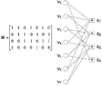
represent code words, corresponds to the columns in PCM, and the check nodes represent parity check equations, which are the row element in PCM. The Tanner graph shows the connection between variable node i and check node j if the corresponding bit hij in the PCM is 1, as shown in the example of Fig. 1.
Fig. 1 Example of parity check matrix and its corresponding Tanner graph.
Gallager introduced the idea of iterative, message passing decoding of LDPC codes . The idea is to iteratively share the results of the local node decoding by passing them along the edges of the tanner graph. The variable node and the check node in parallel, iteratively pass the messages along their adjacent edges. The value of the code bits are updated accordingly.
Based on the domain of analysis, the decoding algorithm are classified as Probability- based sum product algorithm (SPA), Log domain based SPA and LLR domain based SPA[6]. The log-domain SPA algorithm has lower complexity and is more numerically stable than the probability domain SPA algorithm. MS is the modified log domain SPA by replacing product as minimum of sum. The major advantage of MS is that the knowledge of noise power is not needed for the decoding process.
3. MIN-SUM ALGORITHM
MS decoding algorithm [7], is an approximation of the iterative Sum-Product (SP) algorithm. Although the performance of MS is generally a few tenths of a dB lower than that of SP decoding, it is more robust to quantization errors when implemented with fixed-point operations [8] and [9]. In MS the hardware for the check node function is simple when compared to the SP algorithm. In MS decoding, similar to SP algorithm, the extrinsic messages are passed between check and variable nodes in the form of log likelihood ratios (LLRs). The LLR domain is more advantageous than the probability domain decoding because message multiplications are no longer needed. Normalization process used in probability domain requires additional computations. With the use of LLR ratios, these additional computations are eliminated.
3.1.1 ALGORITHM
In the LLR domain, we use the notation L(qij ) for the message passed from the variable node i to check node j, and , and L(rji) for the message from check node j to variable node i. The MS algorithm is described by the following steps in each iterations:
Step 1: The initial messages at variable nodes are set to:
j
y
L(c
i
)
)
ij
L(q
(1)Step 2: Check node update: ) j i' (β i \ Vj i'min ) i \ i'\Vj αi'j ( ) ji L(r
(2)
))
j
i'
sign(L(q
j
i'
α
(3))/
j
i'
/L(q
j
i'
β
(4)Where Vj\i is the set of variable nodes connected to check node j excluding variable node i.
Step 3: Variable node update:
j \ Ci j' L(rj'i) )
i L(c ) ij
L(q (5)
Step 4: Decision at variable nodes:
Ci j L(rji) )
i L(c ) i
L(Q (6)
Where
i
c
is the set of check nodes connected to variablenode i and
i
cˆ
is the estimate of the code bit i. The algorithmstops if (
cˆ
1,...,
cˆ
n
).H
T
=0, or if the maximum number ofiterations is reached.
Step 5: If the conditions above are not satisfied then return to step 1 in the algorithm.
4.
WAVE PIPELINING
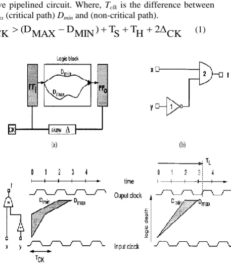
of the signal propagation delay characteristics of the logic network is used at design time to manage the signal delays so as to ensure that operations do not interfere with their predecessor nor successor computations. Fig.2 shows the wave pipelined circuit. Where, Tclk is the difference between Dmax (critical path) Dmin and (non-critical path).
CK 2Δ H T S T ) MIN D MAX (D CK
[image:3.595.67.296.114.382.2]T (1)
Fig.2 Wave pipelining circuit
In the above equation TS and TH are the setup and hold time
which is the same for the circuits. Only the difference in delay of the critical and the non-critical path can be changed. Therefore this procedure of modification is done here. This technique provides a method for significantly reducing clock loads and the associated area, power and latency while retaining the external functionality and timing of a synchronous circuit [11]. It is of particular interest today because it involves design and analysis across a variety of levels (process, layout, circuit, logic, timing, and architecture) which characterize VLSI design. Wave pipelining can improve the throughput of a logic circuit while avoiding some of the overheads of traditional pipelining. The area and power overheads of a traditional pipeline are avoided in the wave pipeline since there are no internal synchronizers.
In order to perform Wave pipelining technique the architecture is designed and analyzed at transistor level to find the critical and non-critical paths. The technique of buffer insertion in the non-critical path is used to realize the Wave pipelined architecture.
5. BUFFER INSERTION
There are number of delay reducing methods. Some of them include Wire Length Minimization, Device Sizing, Buffer Insertion, Wire Size Optimization, Simultaneous Devices and Interconnect Optimization. Buffer Insertion is method used for the reduction of the delay [12]. The minimum and the maximum delay paths are analyzed in the designed architecture. Delay along the maximum and minimum delay path is varied by buffer insertion. Trade off between power consumption and the delay incurred in the architecture. The speed of the designed circuit is improved with the compromise in terms of power consumption.
6. ARCHITECTURE OF MS DECODER
In this paper, for each path the timing analysis had been done. Dmax and Dmin are calculated. The identified non-critical paths are proportionally inserted with buffers. Thereby the Tclk and clock frequency has been evaluated. To implement the variable nodes with degree 3, we use the same basic modules of the architecture designed in [13] and [14].
[image:3.595.311.550.255.713.2]In our design, we calculate the maximum number of bits needed inside the adder module by assuming the maximum values for the inputs. Considering 6-bit quantization, we have 4 inputs with maximum absolute value of „7‟. So the absolute value of the maximum total sum would be „32‟ which can be represented by a 8-bit signed number. Messages are thus converted from 6-bit sign-magnitude to 8-bit 2‟s complement and passed to the full adder. The main advantage of the 2‟s complement conversion is that it leads to reduction in the number of bits in the computation which increases the decoding complexity.
Fig. 3 The architecture of variable node of degree 3 for MS
Also, messages are clipped to
(2
q
1
1)
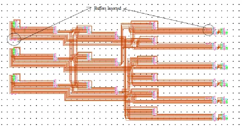
when they are converted back from 8-bit 2‟s complement domain to 6-bit sign-magnitude domain before being passed to the check nodes. The architecture is analyzed in transistor level using T-Spice and the process technology of 45nm is used. The check node architecture consists of two components, one for sign bit and the other for magnitude bits.[image:3.595.314.556.536.717.2]
Fig.4 The schematic of the magnitude update circuit
The messages from the variable nodes have 1 bit for the sign and 5 bits which represent the magnitude. The sign bits of the incoming messages to a check node are XOR-ed together, and then the sign of the outgoing message on each edge is obtained as the XOR of the sign of the incoming variable message on that edge and the XOR of the signs of all the incoming messages.
With the improvement in CNU (Check node update circuit), the buffer insertion technique is also applied to VNU (Variable node update circuit). The effect of buffer insertion is prompt in CNU compared to VNU. The schematic of the magnitude update circuit in Fig.4 shows the description of various minimum and maximum delay paths. The way the buffers are inserted to reduce the difference in delay or Tclk Similar analysis is done in the variable node update circuit. To calculate the magnitude of the messages in check nodes, minimum functions are used. This architecture is shown in Fig.5.
Fig.6 The sign update circuit of check node of degree 6
The sign update circuit is shown in Fig.6. The analyzed result for wave pipelining is before and after buffer insertion is described in table 1 and 2. Results for buffer insertion in the maximum delay path are in table 3.The performance metrics such as the clock frequency, power and delay are analyzed. The optimized architecture operates at a better speed with marginal increase in power.
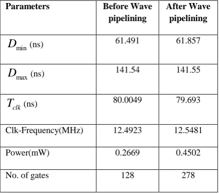
[image:4.595.317.538.513.695.2] [image:4.595.55.283.555.741.2]Table 1 and 2 summarizes the results of the MS and the Wave pipelined MS architecture of the check node and variable node architecture of degree 6 and 5- bit quantization.
Table 1
CNU analysis before and after wave pipelining Parameters Before Wave
pipelining
After Wave pipelining
min
D
(ns) 13.643 81.327max
D
(ns) 201.53 201.53clk
T
(ns) 201.393 200.7167Clk-Frequency(MHz) 4.965 4.9821
Power(mW) 0.525 0.968
No. of gates 708 968
Table 2
VNU analysis before and after wave pipelining Parameters Before Wave
pipelining
After Wave pipelining
min
D
(ns) 61.491 61.857max
D
(ns) 141.54 141.55clk
T
(ns) 80.0049 79.693Clk-Frequency(MHz) 12.4923 12.5481
Power(mW) 0.2669 0.4502
No. of gates 128 278
Table 2 shows that, the speed of the circuit is increased by 55850 Hz with a slight increase in the power consumption after Wave pipelining.
Table 3
CNU analysis before and after buffer insertion in the critical path
Parameters Before buffer insertion
After buffer insertion
min
D
(ns) 61.325 61.325max
D
(ns) 161.39 81.39clk
T
(ns) 100.065 20.067Clk-Frequency(MHz) 9.9935 49.23
Power(mW) 0.525 0.5451
No. of gates 708 960
Table 3 shows that, the speed of the circuit is increased by 49MHz with a slight increase in the power consumption after Buffer insertion. It can be seen from the above analysis that the buffer insertion in the critical path shows a greater improvement in the speed of the circuit with reduced power and number of gates compared to the buffer insertion in the non-critical path.
7. CONCLUSION
The min sum decoder architecture is designed at the transistor level targeted to 45 nm technology. The power and delay parameters are analyzed with the effect of the effect of
buffer insertion at the critical and non-critical path of the designed MS iterative decoder was studied. It is evident that the proposed architecture of buffer insertion at the critical path has improvement in clock frequency/ speed of operation with marginal increase in power. Thereby the efficient hardware architecture is realized with the same decoding performance. The other class of Wave pipelining techniques namely node collapsing and logic restructuring.
REFERENCE
[1] R. G. Gallager, “Low-Density Parity-Check Codes,”. Cambridge MA: MIT Press, 1963.
[2] Keshab K. Parhi, VLSI Digital Signal Processing Systems, Chapter-16, pp 591-642.
[3] Todd K.Moon , Error Correction Coding Mathematical method and Algorithm, Chapter-15, pg 634-674.
[4] William E.Ryan , “An Introduction to LDPC codes” 2003.
[5] Saravanan Swapna , M.Anbuselvi and S.Salivahanan, “Design and analysis of iterative decoder using wave pipelining” Conference proceedings,ICCCE 2012.
[6] Papaharalabos et al, “Modified sum-product algorithms for decoding low-density parity-check codes,” Communications, vol.1, no.3, 2007.
[7] J. Zhao, F. Zarkeshvari and A. H. Banihashemi, “On implementation of min-sum algorithm and its modifications for decoding LDPC codes,” IEEE Trans. Comm., vol. 53, no. 4, pp. 549-554, April 2005.
[8] Sina Tolouei and Amir H. Banihashemi, ―Fpga Implementation Of Variants Of Min-Sum Algorithm,” Dept. of sys.and compt. Engg,caleton university,Ottawa,ON,Canada,2008.
[9] Daesun Oh and Keshab K. Parhi,‖Min-Sum Decoder Architectures With Reduced Word Length for LDPC Codes,”.IEEE Transactions On Circuits And Systems—I: Regular Papers, vol. 57 IET,, no. 1, January 2010. [10] V. Vireen, G. Seetharaman, and B.
Venkataramani,”Synthesis Techniques for Implementation of Wave-Pipelined Circuits in ASICs,” International Conference on Electronic Design, 2008. [11] SurveyWayne P. Burleson, Maciej Ciesielski, Fabian
Klass, and Wentai Liu, “Wave-Pipelining: A Tutorial and Research” IEEE Transactions On Very Large Scale Integration (VLSI) Systems, vol. 6, no. 3, September 1998.
[12] Interconnect Design for Deep Submicron ICs Jason Cong, Zhigang Pan, Lei He, Cheng-Kok Koh and Kei-Yong khoo Computer Science Department University of California, Los Angeles, CA 90095
[13] A.J. Blanksby and C. J. Howland, “A 690-mW 1-Gb/s 1024-b, rate-1/2 low-density parity-check code decoder,” IEEE J. Solid-State Circuits, vol. 37, pp. 404-412, March 2002.