ANALYSIS OF WAVEFUNCTION DISTRIBUTION IN QUANTUM WELL BIASED LASER DIODE USING TRANSFER MATRIX METHOD
E. P. Samuel andD. S. Patil
Department of Electronics North Maharashtra University Jalgaon, Maharashtra, India
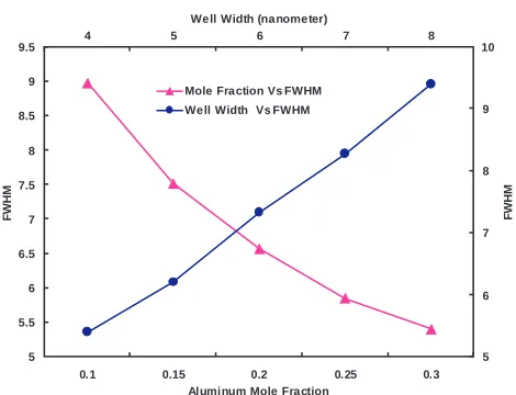
Abstract—The paper presents the faster, simpler, and accurate algorithm to solve time independent Schr¨odinger equation based on transfer matrix method. We can thus calculate all bound and quasi bound energy and the corresponding probability density. A central part of this paper deals with the solving of Schr¨odinger equation for quantum well structure. Our results show that the transfer matrix method is accurate, it is easier to implement. The increase in well width increases the FWHM from 5.4 nanometer to 9.4 nanometer, while the increase in the Aluminum concentration the FWHM decreases from 8.98 to 5.4.
1. INTRODUCTION
In recent years semiconductor quantum wells have attracted growing interest for laser applications mainly due to their potential for a reduction of the threshold current density, and their increased gain and differential gain achieved by confinement. Since, quantum confinement of carriers in semiconductor quantum wells [1–7] leads to quantized subband energies. Parallel to the effort concerning the fabrication and characterization of quantum wells, their theoretical modeling are developed with increasing level of sophistication, in order to enable the prediction of the physical properties of such structures and to enable a deeper understanding of experimental results.
emitting devices. The III-V nitride semiconductors GaN, AlN, and their ternary alloys are highly attractive due to their great potential for development of shorter wavelength optoelectronic devices. Even though, remarkable progress in growth of GaN and their alloys and in fabrication technology of the devices using these materials, some basic properties of GaN/AlGaN still remain poorly studied [8–13].
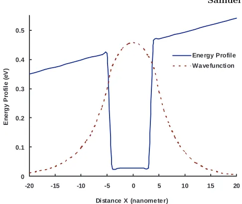
In this paper we present a simple, accurate, and fast algorithm for numerically solving the Schr¨odinger equation for quantum well structure as shown in Figure 1. The wavefunction and Eigen energy profile under an applied electric field is as shown in Figure 2. The Eigen energy and wavefunction are obtained by the algorithm based on the transfer matrix method (TMM) [14–18]. The TMM is a general numerical method that can be used for a wide range of problems dealing with second order differential equations. One example is the calculation of propagation characteristics in planar wave guide, presented by Walpita [19]. One other example of the transfer matrix method is given in [20, 21], where the spontaneous emission in a DFB laser is investigated. The TMM is simple to implement and gives accurate results to three or four digits which is more than sufficient for most applications and this method gives quick and accurate answers to complex problems.
This paper is outline as follows, in Section 2, we will give a brief explanation of the theory behind the transfer matrix method and its implementation. Section 3 contains several examples of results obtained with our program carried out for single quantum well structure in an applied electric field and takes the variation of well width and the effective mass with varying Aluminum mole fraction in AlxGa1−xN. Finally, in Section 4 we present the conclusions.
2. SIMULATION MODEL
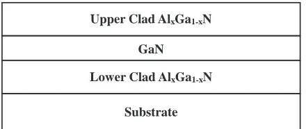
Substrate Lower Clad AlxGa1-xN
GaN
Upper Clad AlxGa1-xN
Figure 1. GaN/AlxGa1−xN based quantum well structure laser diode.
composition [25, 26].
For our simulation we had considered the simple quantum structure as shown in Figure 1. From Figure 1 it is clearly observed that under biased condition the barrier height at the two interfaces are different. To analyze the quantization effect in quantum structure we had solved the Schr¨odinger equation by using Transfer matrix method. The time independent Schr¨odinger equation with an electric filed is given as follows
− h
4m∗π
∂2ψ(x)
∂x2 +V(x)ψ(x) =Eψ(x) (1)
where, m∗ is the effective mass, h, is the Planck’s constant,E, is the Eigen energy
V(x) =− |e|φ(x) +Vc(x) +|e|F z (2)
At this juncture, e is the electron charge, Vc is the square well
potentials for the conduction band, F is the applied electric field, here, φ is assumed to be zero for our calculation. The envelope wavefunction ψ(x) of Schr¨odinger equation when solved with an appropriate boundary conditions the general solution for quantum well and barrier region obtained are given by Equations (3a) to (3b) as follows.
ψI(x) = A1eik1x+A2e−ik1x (3a)
ψII(x) = B1cos (k2x) +iB2sin (k2x) (3b)
ψIII(x) = C1eik1x+C2e−ik1x (3c)
0 0.1 0.2 0.3 0.4 0.5
-20 -15 -10 -5 0 5 10 15 20
Distance X (nanometer)
En e rg y Pr o fi le ( e V) Energy Profile Wavefunction
Figure 2. Energy profile and Wavefunction as function of distance X.
function at interface to be equal according to the boundary conditions are as follows.
M1
A1
A2
=M2
B1 B2 (4a) and M3 B1 B2 =M4
C1
C2
(4b)
While M1,M2,M3,M4, are given by the following expressions.
M1 =
e−k1a ek1a
k1e−ka −k1eka
, (5a)
M2 =
cos (k2a) −sin (k2a)
k2sin (k2a) k2cos (k2a)
(5b)
M3 =
cos (k2a) sin (k2a) −k2sin (k2a) k2cos (k2a)
(5c)
M4 =
ek1a e−k1a
k1eka −k1e−ka
(5d)
transmission coefficient of the quantum well structure based laser diode. The Eigen energy is necessary for the determination of the wave vectors of the quantum well and barrier region. The probability density, confinement factor and other electrical properties, thus the transfer matrix method provides a number of electrical properties efficiently and accurately.
A1
A2
=M1−1M2M3−1M4
C1
C2
(6)
3. RESULTS AND DISCUSSION
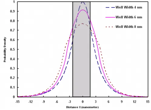
There has been great in the high speed modulation of semiconductor laser sources used mainly for large capacity optical communication system. More recent developments include the field induced gain switching of semiconductor lasers. Hence, we tried to carry out the analysis of single quantum well structure Gallium Nitride based laser diode under an applied electric field. The analysis has been carried out for varying well width and different Aluminum mole fraction under biased conditions. We, assumed 5 V potential across the quantum well laser diode.
Figure 3. Probability density for varying well width vs distance X.
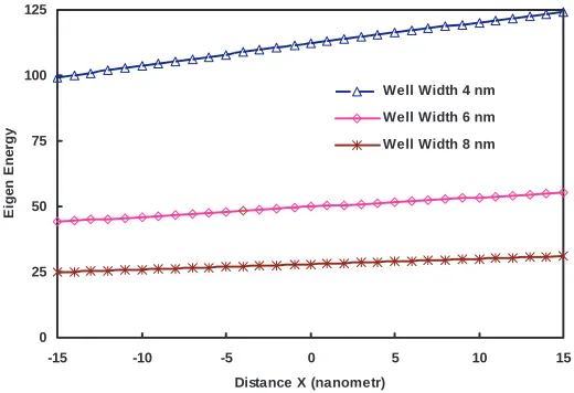
From figure it is clearly observed that for the narrower well width the probability has maximum amplitude, while with increase of the well width amplitude decreases. An important observation from Figure 3 is that the wavefunction grows sharply for narrow quantum wells, while for broader well width the wavefunction are not much sharper. The sharpness of the wavefunction for well width of 4 nm is due to the fact that Eigen energy is much higher i.e., 100 meV and above along with the length of the device as observed in Figure 4. The Eigen energy increases almost linear along the X-axis, and decreases with the increase in well width.
0 25 50 75 100 125
-15 -10 -5 0 5 10 15
Distance X (nanometr)
E
ige
n E
n
e
rgy
Well Width 4 nm
Well Width 6 nm
Well Width 8 nm
Figure 4. Eigen energy for different well width for corresponding position in quantum structure.
non-Figure 5. Probability density for varying aluminum concentration vs distance X.
0 26 52 78 104 130
-20 -15 -10 -5 0 5 10 1 20 Distance X (nanometer)
E
ige
n E
n
e
rgy
(
m
e
V
)
Aluminum Mole Fraction 0.1
Aluminum Mole Fraction 0.2
Aluminum Mole Fraction 0.3
5
Figure 6. Eigen energy for different aluminum concentration for corresponding position in quantum structure.
5 5.5 6 6.5 7 7.5 8 8.5 9 9.5
0.1 0.15 0.2 0.25 0.3
Aluminum Mole Fraction
FW
H
M
5 6 7 8 9 10
4 5 6 7 8
Well Width (nanometer)
FW
H
M
Mole Fraction Vs FWHM Well Width Vs FWHM
Figure 7. FWHM of the probability density as function of well width and aluminum mole fraction.
4. CONCLUSIONS
The transfer matrix method is faster, accurate, and simpler to implement it for the solution of the Schr¨odinger equation. The Eigen energy has been deuced for different Aluminum mole fraction and well widths. The Eigen energy variation observed to be from 13.69 meV to 129.38 meV. The applied electric field in the quantum structure causes the variation in the Eigen energy along theXaxis shows a vast variation.
REFERENCES
1. Samuel, E. P. and D. S. Patil, “Effect of aluminum mole fraction and well width on the probability density spreading in GaN/AlGaN quantum well,” Optoelectronics and Advanced Materials-Rapid Communications, Vol. 8, 394, 2007.
2. Chiu, C. H., H. C. Kuo, C. E. Lee, C. H. Lin, P. C. Cheng, H. W. Huang, T. C. Lu, S. C. Wang, and K. M. Leung, “Fabrication and characteristics of thin film InGaN-GaN light emitting diodes with TiO2/SiO2 omnidirectional reflectors,”
Semiconductor Science and Technology, Vol. 22, 831, 2007. 3. Chen, C.-N., K.-F. Yarn, W.-J. Luo, et al., “Effects of giant optical
4. Ahmed, I. and A. R. Baghai-Wadji, “1D canonical and perturbed quantum potential wave problem: A universal approach,”PIERS Online, Vol. 3, 481, 2007.
5. Chen, C.-N., W.-C. Chien, K.-F. Yarn, S.-H. Chang, and M.-L. Hung, “Intrinsic optical anisotropy in Zinc-blende semiconduc-tor quantum wells,”Progress In Electromagnetics Research Sym-posium, 223, Hangzhou, China, August 22–26, 2005.
6. Brubach, J., A. Y. Silov, J. E. M. Haverkort, W. van der Vleuten, and J. H. Wolter, “Carrier capture in ultrathin InAs/GaAs quantum wells,”Physical Review B, Vol. 61, 136833, 2000. 7. Peng, L.-H., C.-M. Lai, C.-W. Shih, C.-C. Chuo, and
J.-I. Chyi, “Boundary effects on the optical properties of InGaN multiple quantum wells,”IEEE J. of Selected Topics in Quantum Electronics, Vol. 9, 708, 2003.
8. Baro, M., H. Chr. Kaiser, H. Neidhardt, and J. Rehberg, “Dissipative Schr¨odinger-Poisson systems,” J. of Mathematical Physics, Vol. 45, 21, 2004.
9. Gmachl, C., D. L. Sivco, R., F. Colombelli, F. Capasso, and A. Y. Cho, “Ultra-broadband semiconductor laser,” Letters to Nature, Vol. 415, 883, 2002.
10. Samuel, E. P., K. Talele, U. Zope, and D. S. Patil, “Semi-classical analysis of capture in Gallium Nitride quantum wells,”
Optoelectronics and Advanced Materials-Rapid Communications, Vol. 5, 221, 2007.
11. Shwetanshumala, S. Jana, and S. Konar, “Propagation of a mixture of modes of a laser beam in a medium with saturable nonlinearity,” J. of Electromagn. Waves and Appl., Vol. 20, 65, 2006.
12. Mora-Ramos, M. E., R. Perez-Alvarez, and V. R. Velasco, “The electrostatic potential associated to interface phonon modes in Nitride single heterostructures,” Progress In Electromagnetics Research Letters, Vol. 1, 27, 2008.
13. Hori, A., D. Yasunaga, A. Satake, and K. Fujiwara, “Temperature and injection current dependence of electroluminescence intensity in green and blue InGaN single quantum well light emitting diodes,”J. of Applied Physics, Vol. 93, 3152, 2003.
15. Chern, G. D., H. E. Tureci, A. D. Stone, R. K. Chang, M. Kneissl, and N. M. Johnson, “Unidirectional lasing from InGaN multiple quantum well spiral-shaped micropillars,”Applied Physics Letters, Vol. 83, 1710, 2003.
16. Mamishev, A. V., K. S. Rajan, F. Yang, Y. Du, and M. Zahn, “Interdigital sensors and transducers,” Proceedings of the IEEE, Vol. 92, 808, 2004.
17. Srivastav, R., S. Pati, and S. P. Ojha, “Enhancement of omnidirectional reflection in photonic crystal heterostructures,”
Progress In Electromagnetics Research B, Vol. 1, 197, 2008. 18. Walpita, L. M., “Solutions for planar optical waveguide equations
by selecting zero elements in a characteristic matrix,”J. Opt. Soc. Amer. A, Vol. 2, 595, 1985.
19. Brennan, K. E. and C. J. Summers, “Theory of resonant tunneling in a variably spaced multiquantum well structure: An airy function approach,”J. Appl. Phys., Vol. 61, 614, 1987.
20. Ghatak, A. K., K. Thyagarajan, and M. R. Shenoy, “A novel numerical technique for solving the one-dimensional Schr¨odinger equation using matrix approach application to quantum well structures,”IEEE J. Quantum Electron., Vol. 24, 1524, 1988. 21. Lu, J., B. I. Wu, J. A. Kong, and M. Chen, “Guided modes with
a linearly varying transverse field inside a left-handed dielectric slab,” J. of Electromagn. Waves and Appl., Vol. 20, No. 5, 689, 2006.
22. Gaggero-Sager, L. M., N. Moreno-Martinez, I. Rodriguez-Vargas, R. Perez-Alvarez, V. V. Grimalsky, and M. E. Mora-Ramos, “Electronic structure as a function of temperature for Siδ-doped quantum wells in GaAs,”PIERS Online, Vol. 3, No. 6, 851, 2007. 23. Gaggero-Sager, L. M. and I. Rodriguez-Vargas, “p-n-p δ-doped Quantum Wells in GaAs,”PIERS Online, Vol. 3, No. 6, 855, 2007. 24. Chen, C.-N., K.-F. Yarn, W.-C. Chien, S.-H. Chang, and M.-L. Hung, “Interface heterobond effects in (hkl) InAs/GaSb super-lattice solved by bond orbital model,”Progress In
Electromagnet-ics Research Symposium, 318, Hangzhou, China, August 22–26,
2005.
25. Jancewicz, B., “Plane electromagnetic wave in PEMC,” J. of Electromagn. Waves and Appl., Vol. 20, No. 5, 647, 2006.
26. Wu, C.-J., “Transmission and reflection in a periodic supercon-ductor/dielectric film multilayer structure,” Progress In
Electro-magnetics Research Symposium, 164, Hangzhou, China, August