ABSTRACT
VAN DEN BROECK, DENNIS MARNIX. Engineering Strain for Improved III-Nitride
Optoelectronic Device Performance. (Under the direction of Dr. Salah Bedair and Dr. Nadia El-Masry).
Due to growing environmental and economic concerns, renewable energy
generation and high-efficiency lighting are becoming even more important in the scientific
community. III-Nitride devices have been essential in production of high-brightness
light-emitting diodes (LEDs) and are now entering the photovoltaic (PV) realm as the technology
advances. InGaN/GaN multiple quantum well LEDs emitting in the blue/green region have
emerged as promising candidates for next-generation lighting technologies. Due to the large
lattice mismatch between InN and GaN, large electric fields exist within the quantum well
layers and result in low rates of radiative recombination, especially for the green spectral
region. This is commonly referred to as the “green gap” and results in poor external
quantum efficiencies for light-emitting diodes and laser diodes. In order to mitigate the
compressive stress of InGaN QWs, a novel growth technique is developed in order to grown
thick, strain-relaxed InyGa1-yN templates for 0.08 < y < 0.11. By inserting 2 nm GaN interlayers into the growing InyGa1-yN film, and subsequently annealing the structure, “semibulk” InGaN templates were achieved with vastly superior crystal and optical
properties than bulk InGaN films. These semibulk InGaN templates were then utilized as
new templates for multiple quantum well active layers, effectively reducing the
compressive strain in the InGaN wells due to the larger lattice constant of the InGaN
template with respect to a GaN template. A zero-stress balance method was used in order
optical characteristics when compared to fully-strain active regions. The semibulk InGaN
template was then implemented into “strain-compensated” LED structures, where light
emission was achieved with very little leakage current. Discussion of these
Engineering Strain for Improved III-Nitride Optoelectronic Device Performance
by
Dennis Marnix Van Den Broeck
A dissertation submitted to the Graduate Faculty of North Carolina State University
in partial fulfillment of the requirements of the degree of
Doctor of Philosophy
Electrical Engineering
Raleigh, North Carolina 2016
APPROVED BY:
______________________ ______________________ Dr. Salah Bedair Dr. Nadia El-Masry
Committee Chair
ii
Dedication
iii
Biography
Dennis Marnix Van Den Broeck was born in the small Los Angeles suburb known as
Sunland on September 25th, 1989. His father, Herman Van Den Broeck, owned the vegetable import/export business known as Coosemans LA and his mother, Hedwig Van
Den Broeck, was a computer programmer turned mother of four. Due to his father’s
business ventures, Dennis moved around the country almost every four years. He spent his
early years in the Florida Keys, then attended half of elementary school in Walnut Creek,
California. He then moved to Miami, Florida for the second half of elementary school,
followed by middle school in Lexington, Kentucky when his father retired. Dennis then
attended the McCallie School for highschool in Chattanooga, Tennessee and finally wound
up in Raleigh, North Carolina to attend North Carolina State University for college. Raleigh
ended up grounding Dennis’s interests as he lived there for almost 10 years, met many
friends, entered graduate school and met the love of his life, Lauren Powell. Dennis began
his Ph.D studies in January of 2012 by joining the research group of Dr. Salah Bedair and Dr.
iv
Acknowledgements
I would first like to thank both Dr. Salah Bedair and Dr. Nadia El-Masry, who
provided an opportunity for me to grow into the scientist I am today. I have become a
better equipped individual to take on the real world thanks to the time that I had in the lab.
For Dr. Bedair, I’d like to thank for the hours of conversations, both technically relevant and
random. His approach to engineering difficulties has been an inspiration. For Dr. El-Masry,
I’d like to thank for the patience and mentoring, especially when the lab was in difficult
times. Her presence always seemed to get the lab moving again.
Thanks to Dr. Leda Lunardi and Dr. Robert Trew for serving on my Ph.D Committee
and providing valuable feedback. I would also like to thank Dr. Mehmet Ozturk for an
important substitution.
Thanks to Aadhitya Hosalli, my senior, who provided me with the tools necessary to
achieve success in the lab. To Dr. Colter, who was my go-to man for any reactor
troubleshooting or inquiries. To Deon and Zhenyu, who taught me that you don’t learn
everything in the class or in the lab. To Geoff Bradshaw, Zach Carlin, Brandon Hagar and
Islam Sayed, the RB II Crew, who were always ready to help.
Thanks to my friends and family, who I would not have been able to survive without.
Thanks to my mother, Hedwig, for never giving up on me. And thanks to my fiancé, Lauren,
v
Table of Contents
List of Tables………..………vii
List of Figures……….…….viii
Chapter 1: Introduction 1.1Motivation………..…….1
1.2Nitride Semiconductors and Optoelectronic Devices………...1
1.3Issues with III-Nitride Growth………..…..4
1.4Polarization in Nitrides and QCSE………..……..9
1.5References………..……..13
Chapter 2: MOCVD System and GaN Growth, Fabrication and Characterization 2.1Introduction………..14
2.2Description of the MOCVD System………14
2.3GaN Growth Procedure……….16
2.4Device Fabrication……….19
2.5Structural Characterization: X-ray Diffraction………22
2.6Structural Characterization: Electron Microscopy………..24
2.7Optical Characterization: Photoluminescence and Electroluminescence………25
2.8References………..……..27
Chapter 3: InxGa1-xN Growth and Characterization 3.1Introduction………..28
3.2InxGa1-xN Growth Obstacles………28
3.3InxGa1-xN Growth Procedure………..35
3.4INxGa1-xN Film Characterization………36
3.5References………..………..39
Chapter 4: High-Quality, Relaxed InyGa1-yN Templates 4.1Introduction………..41
4.2Relaxation Mechanisms of InxGa1-xN Grown on GaN………41
4.3“Bulk” InxGa1-xN Film Growth and CLT Determination……….44
4.4“Semibulk” InxGa1-xN………..46
4.5Semibulk InxGa1-xN Characterization………..………….49
4.6Optoelectronic Applications of Semibulk InxGa1-xN Layers………..……...56
4.7Conclusions………..……… 58
vi Chapter 5: Strain-balanced InGaN/GaN Multiple Quantum Wells
5.1Introduction………..63
5.2The Role of Strain in InGaN/GaN Quantum Well Emission………..63
5.3Engineering Strain: Strain-balanced Multiple Quantum Wells………..64
5.4Strain-balanced MQW Characterization………68
5.5Optoelectronic Applications of SBMQWs……….71
5.6Conclusions………72
5.7References……….74
Chapter 6: Modelling of InGaN QW and SBMQW Structures 6.1Introduction………..76
6.2Band Gap Model for Conventional InGaN Quantum Wells………..76
6.3Band Gap Model for SBMQWs……….82
6.4Band Gap Simulation Using nextnano3………..84
6.5Conclusions………88
6.6References……….89
Chapter 7: Strain-Compensated LEDs 7.1Introduction………..90
7.2LED Efficiency………90
7.3Strain-Compensated LEDS Grown on Relaxed Semibulk InGaN Templates…………..94
7.4Strain-Compensated LED Characterization………..………..97
7.5Strain-Compensated LED Discussion……….100
7.6Conclusions……….……103
7.7References………..…104
Chapter 8: Conclusion 8.1Dissertation Summary……….……106
8.2Future Work………..…………..…….107
vii
List of Tables
Table 1.1: Relevant physical, mechanical and electronic properties of III-nitride compound semiconductors as well as other compounds.
Table 1.2: Ionization energies of III-nitride compounds as well as other relevant semiconductor compounds.
Table 4.1: Summary of the bulk and semibulk InGaN test structures referenced in this chapter. Bi are related to the conventional bulk InxGa1-xN structures whereas SBi are related to the semibulk InxGa1-xN structures.
Table 4.2: Hall Effect results of the 300 nm semibulk InxGa1-xN layer grown on an insulating GaN/sapphire template.
Table 5.1: Summary of the samples grown for this experiment. SBMQWi are related to the SBMQW structures grown on InyGa1-yN temples, while MQWi are the conventional MQW structures grown on GaN tempaltes.
Table 6.1: Simulation parameters for the nextnano3 simulation software used for this work. Input files are displayed in the appendix.
viii
List of Figures
Figure 1.1: Bandgap vs. lattice constants for III-V (blue markers) and II-VI (green and pink) compound semiconductors.
Figure 1.2: Schematic of a conventional blue-emitting InxGa1-xN MQW LED structure
consisting og an n-GaN base, p-GaN emitter, and InxGa1-xN/GaN MQW active region grown on a sapphire substrate.
Figure 1.3: Ionization energy of Mg vs. indium composition in InxGa1-xN.
Figure 1.4: Atomic arrangement and direction of spontaneous polarization for wurtzite GaN that is a) Ga-polar and b) N-polar.
Figure 1.5: Spontaneous (PSP) and piezoelectric (PPZ) field directions for (upper) unstrained GaN, (middle) tensile-strained AlGaN, and (lower) compressive-strained InGaN. Ga-polarity is at the top of each structure.
Figure 1.6: Calculated band profiles for 5nm/10nm GaN/Al0.1Ga0.9N quantum wells, which take into accound both strain and coulomb interaction for a) c-plane [0001] quantum wells and b) m-plane [1-100] nonpolar quantum wells. Calculated electron and hole wave
functions are superimposed onto the band profiles.
Figure 2.1: a) Photo of the MOCVD system during GaN growth, b) simplified schematic of the MOCVD growth chamber.
Figure 2.2: Schematic diagram of the III-column run/vent manifold.
Figure 2.3: Photo of the 8' x 8' modular cleanroom in our laboratory.
Figure 2.4: Schematic of device isolation fabrication detailed in steps 1 - 11 above
Figure 3.1: Equilibrium vapor pressure of N2 over AlN, GaN and InN. From [4].
Figure 3.2: Variation of InxGa1-xN/GaN heterostructure CLT with indium content x. From [11].
Figure 3.3: Indium content map of an In0.16Ga0.84N/GaN sample obtained from the interpolation of 200 EDX measurements from the InGaN/GaN interface to the InGaN surface. Indium content is distinguished by the warm colors, where deep red is 30% InN. From [12].
Figure 3.4: SEM image of the surface of a thick InxGa1-xN layer undergoing elastic
ix Figure 3.5: Temperature vs. InN composition x phase diagram for InxGa1-xN films. The solid curve indicates the binodal curve while the dashed indicates the spinodal. From [16].
Figure 3.6: θ/2 θ XRD scans of a 100 nm (black curve) strained InxGa1-xN film and 200 nm (red curve) relaxed InxGa1-xN film grown on GaN/sapphire substrates.
Figure 3.7: Room temperature PL emission of a 100 nm strained InxGa1-xN film (black curve) and a 200 nm relaxed InxGa1-xN film (red curve).
Figure 4.1: TEM image of a 60 nm In0.12Ga0.88N film grown on a GaN template revealing the presence of three distinct layers. The dashed white arrows indicated the transition from the pseudomorpically strained first InGaN sublayer to the inhomogeneous second InGaN sublayer. From [12].
Figure 4.2: InN compositional dependence on growth temperature for InxGa1-xN films grown by our MOCVD.
Figure 4.3: Variation in PL peak emission energy with respect to film thickness of In0.08Ga0.92N and In0.15Ga0.85N films grown on GaN templates. From [6].
Figure 4.4: Schematic diagrams of the semibulk InxGa1-xN sublayer growth process. a) An InxGa¬1-xN sublayer is grown to the transition thickness for indium accumulations (blue circles), b) a thin GaN interlayer (yellow region) is then grown to absorb/desorb
accumulating indium, c) a spike anneal is then performed at 1000 °C to planarize the growth surface.
Figure 4.5: Schematic diagrams of a) the bulk InxGa1-xN control test structure, and b) the semibulk InxGa1-xN test structure. Inset: expanded view of the semibulk InxGa1-xN growth layers.
Figure 4.6: Normalized PL spectra obtained from the relaxed InxGa1-xN samples with intended x = 0.11.
Figure 4.7: θ/2θ XRD scans of the relaxed bulk (black curve) and semibulk (red curve) InxGa1-xN samples with intended x = 0.11.
Figure 4.8: Plan-view SEM images of a) the bulk InxGa1-xN surface revealing 3D growth and V-pitting, b) the semibulk InxGa1-xN surface devoid of V-pits. Both images are captured at 25,000x magnification. c) Enlarged image of the semibulk InxGa1-xN surface. Enlargement shows some surface features, which are attributed to non-uniform growth rates on the sample surface. Image was captured at 50,000x magnification.
x Figure 4.10: Plot of the double crystal XRD rocking curve FWHM of (hkil) planes as a function of the lattice plane inclination angle φ. The inclination angle is between the c-axis and the normal axis of the particular crystallographic plane.
Figure 5.1: Schematics of a) the proposed InxGa1-xN/GaN SBMQW structure grown on an InyGa1-yN semibulk template with x >y and b) the conventional InxGa1-xN/GaN MQW structure grown on GaN.
Figure 5.2: Normalized PL spectra of a) 2 and 10 period conventional InxGa1-xN/GaN MQW structures grown on GaN templates with x = 0.16, b) 2 and 10 period InxGa1-xN SBMQW structures grown on 180 nm InyGa1-yN semibulk templates for x = 0.16 and y = 0.08, c) 10 period InxGa1-xN/GaN SBMQW structures grown on 180 nm InyGa1-yN templates for x = 0.16, 0.2 and 0.22 and y = 0.08, 0.1 and 0.11, respectively.
Figure 6.1: Band gap energy vs. QW InN percentage (x) of relaxed (solid blue line) and strained (dashed orange line) InxGa1-xN.
Figure 6.2: InGaN QW band gap shift vs. QW width due to quantization from QSE.
Figure 6.3: Peak wavelength versus InxGa1-xN QW InN percentage (x) for a conventional MQW structure. A 2 nm QW width is assumed for these calculations.
Figure 6.4: Peak wavelength versus InxGa1-xN well composition for the conventional MQW model (blue line) and experimental results (yellow circles) and for the SBMQW model
(orange line) and experimental results (green circles). A 2 nm QW width is assumed for these calculations. Experimental results are of 2 periods MQW and SBMQW samples.
Figure 6.5: Schematics of the structures simulated with the nextnano3 software. a) The conventional InxGa1-xN MQW structure grown on GaN, b) the InxGa1-xN SBMQW structure grown on a strain-relaxed InyGa1-yN template. Simulation parameters can be found in Table 6.1.
Figure 6.6: Nextnano3 band gap simulations of the structures shown in Figure 5.5. a) The conventional InxGa1-xN/GaN MQW structure grown on GaN, b) the InxGa1-xN SBMQW structure grown on a strain-relaxed InyGa1-yN template.
Figure 6.7: Simulations of the strain tensor and electric field using nextnano3. a) Strain tensor for the conventional InxGa1-xN/GaN MQW structure on GaN showing all strain is confined in the wells, b) strain tensor for the InxGa1-xN/GaN SBMQW structure on the InyGa1-yN template showing the strain-balance between the InxGa1-xN wells and GaN barriers, c) electric field of the conventional InxGa1-xN/GaN structure grown on GaN, d) electric field of the InxGa1-xN/GaN SBMQW structure grown on InyGa1-yN template.
xi Figure 7.2: Escape cone for light generated within an LED assuming an arbitrary point source and a material index of refraction n > 1.0.
Figure 7.3: Device schematics of a) Conventional A containing 4x MQW active region, b) Conventional B containing 1x SQW active region, c) Conventional C containing 4x MQW active region a 20 nm AlGaN:Mg electron blocking layer.
Figure 7.4: Device schematics of a) SC-LED A containing 4x MQW active region and GaN:Mg p-type layer, b) SC-LED B containing 4x MQW active layer and In0.08Ga0.92N p-type layer, c) SC-LED C containing 4x MQW active region and In0.16Ga0.84N p-type layer.
Figure 7.5: Photograph of a probed, fully-fabricated device sample under forward bias for EL measurements. Each sample contains 81 separate devices and light is collected through the sapphire underneath the sample.
Figure 7.6: EL emission spectra of SC-LED A under a) DC forward bias and b) pulsed forward bias. Pulsed current duty cycle was 1 ms on 1 ms off.
Figure 7.7: a) EL peak emission wavelength shift versus injected current, b) EL emission FWHM versus injected current.
1
Chapter 1: Introduction
1.1 Motivation
Due to growing environmental and economic concerns, renewable energy generation
and high-efficiency lighting are becoming even more important in the scientific community.
III-nitride devices have been essential in production of high-brightness LEDs and are now
entering the photovoltaic (PV) realm as the technology advances. The motivation for this
dissertation work is to improve the quantum efficiency of III-nitride light-emitting diode (LED)
devices through crystal strain engineering for better product efficiency in the solid-state
lighting (SSL) industry.
1.2 Nitride Semiconductors and Optoelectronic Devices
III-nitride compound semiconductors have been heavily investigated for the past 20+
years due to the tunable direct bandgap of the AlInGaN material system. Initially, III-nitrides
were explored for optoelectronic applications such as LEDs, laser diodes (LDs), PVs and p-i-n
photodiodes, and are poised to take over the multi-billion dollar SSL industry. More recently,
III-nitrides have found applications in microelectronic applications such as radio-frequency
devices, high-power switches and transistors. Wide bandgap III-V semiconductors have a host
of properties that make them an ideal material for these applications, such as the direct
bandgap, high breakdown voltage, large effective masses and exciton binding energy, and
high chemical stability. However, high-brightness LEDs are currently the primary application
of III-nitride devices. Figure 1.1 shows the bandgap and lattice constant range for a host of
2
combined in order to form AlxGa1-xN and InxGa1-xN ternary compounds which have bandgaps that span from 0.7 eV (InN, infrared) to 6.2 eV (AlN, deep UV), a much larger range than the
arsenides and II-VI compounds. Table 1.1 summarizes some of the other advantages of
III-nitrides, as well as some basic physical parameters of compound semiconductors2,3.
The first high-brightness III-nitride LEDs, emitting in the blue, yellow and green
spectral regions, were demonstrated by Nakamura in 1995 using an InGaN/GaN multiple
quantum well (MQW) LED structure4. This structure consists of InGaN/GaN MQWs sandwiched by a GaN PN junction and has become the conventional method in realizing LEDs
in the SSL industry. Figure 1.2 shows a schematic of the conventional InGaN/GaN MQW LED
structure. This device was later used in LDs by incorporating waveguides into the design5.
There are currently three distinct approaches for producing white light LEDs for SSL
purposes. The most common approach utilizes a blue-emitting InGaN/GaN LED coated with
a thin phosphor. This phosphor converts some of the LED emission into a broadband yellow
3
emission, therefore “tricking” our eyes into seeing white light. This approach, however, has
some inherent losses due to the conversion of the light emission wavelength, therefore
producing heat. The second approach is similar to the first, but instead uses an ultraviolet
(UV) GaN-based LED with a phosphor coating. This LED is coated with three different
phosphors emitting in the red, green and blue spectral reasons. Again, this method suffers
from the same inherent losses from light conversion. The third approach involves
incorporating three separated LED devices (red, blue and green) and combining the emission
to create a pixel. This approach has seen commercial success in the display industry, but has
been too costly for SSL. Although InGaN LEDs emit very efficiently in the blue region, the
quantum efficiency plummets as the emission wavelength is pushed to
4 1.3 Issues with III-Nitride Growth
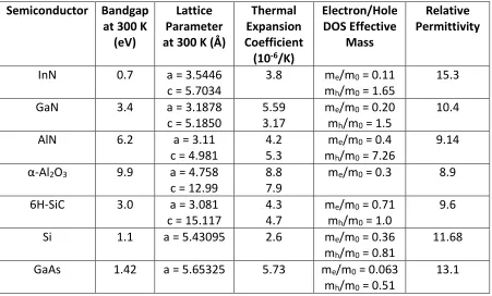
Table 1.1 Relevant physical, mechanical and electronic properties of III-nitride compound semiconductors as well as other compounds.
Before 1991, GaN growth on sapphire substrates exhibited poor crystalline quality
and was therefore not investigated heavily. Nakamura then introduced a low temperature
GaN buffer layer which yielded high quality, specular GaN films on sapphire templates6. This work incited researches to pursue GaN research again, propelling GaN-based LEDs to
dominate the SSL industry. Semiconductor Bandgap
at 300 K (eV)
Lattice Parameter at 300 K (Å)
Thermal Expansion Coefficient
(10-6/K)
Electron/Hole DOS Effective
Mass
Relative Permittivity
InN 0.7 a = 3.5446
c = 5.7034
3.8 me/m0 = 0.11 mh/m0 = 1.65
15.3
GaN 3.4 a = 3.1878
c = 5.1850
5.59 3.17
me/m0 = 0.20 mh/m0 = 1.5
10.4
AlN 6.2 a = 3.11
c = 4.981
4.2 5.3
me/m0 = 0.4 mh/m0 = 7.26
9.14
α-Al2O3 9.9 a = 4.758
c = 12.99
8.8 7.9
me/m0 = 0.3 8.9
6H-SiC 3.0 a = 3.081
c = 15.117
4.3 4.7
me/m0 = 0.71 mh/m0 = 1.0
9.6
Si 1.1 a = 5.43095 2.6 me/m0 = 0.36
mh/m0 = 0.81
11.68
GaAs 1.42 a = 5.65325 5.73 me/m0 = 0.063
mh/m0 = 0.51
5
Although III-nitride optoelectronics have been in development since the early 1990’s,
the material system is still considered in its infancy due to the litany of material and device
challenges. Due to the scarcity of native substrates, III-nitrides have typically been grown
heteroepitaxially on [0001] c-plane sapphire or SiC. They are therefore subject to undesirable
conditions for proper crystal growth, i.e. lattice constant and thermal coefficient mismatches.
Heteroepitaxy of GaN on sapphire/SiC therefore results in a high density (107 – 1010 cm-2) of crystal defects, such as atomic vacancies, threading dislocations and crystal mosaicity7. This high dislocation density results in degradation of device performance, such as low quantum
efficiency in LEDs and prematurely low breakdown voltages in field-effect transistors (FETs).
The large exciton binding energy and effective mass of III-nitride materials, however, reduces
the impact of high dislocation densities due to the very small size of the III-nitride Bohr radius
for excitons8. There has been considerable effort in developing native substrates, such as bulk GaN9,10 and bulk AlN11, where defect densities have been reduced to the 103 cm-2 range, but ultimately these substrates are commercially unviable due to high cost and limited wafer
sizes.
6
Additional to the challenges in GaN/sapphire template growth are issues arising in the
growth of the AlxGa1-xN and InxGa1-xN ternaries on these templates. Due to the use of heteroepitaxy, AlxGa1-xN/GaN and InxGa1-xN/GaN interfaces generate and even higher density of defects than the GaN/sapphire template. Other factors, such as parasitic pre-reactions and
limited surface lifetime also make growing these ternary compounds difficult.
Due to its viability in the SSL industry, the InxGa1-xN ternary has received a large amount of attention. Nevertheless, this compound has been especially challenging to grow
due to some fundamental growth issues. Firstly, significantly lower growth temperature is
required to grow InxGa1-xN films due to the weak In-N bonds as well as the possibility of In atoms desorbing from the growing surface12. These low temperatures yield poor quality films due to impurity incorporation and low surface mobility, and place a severe limitation on the
incorporation of indium into the InxGa1-xN film. The inability to use hydrogen as a carrier gas also limits InxGa1-xN films as hydrogen is typically used to aid in epitaxial growth13. It is speculated that the hydrogen may have an effect on the surface lifetime of the indium atom,
therefore limiting the indium incorporation. Phase separation is also apparent in InxGa1-xN films, especially in films with large x values. This makes compositional control of InxGa1-xN films difficult.
Conductivity control is also a defining characteristic of semiconductor materials.
Typically done by incorporating impurity atoms, the intentional dopants form energy states
within the semiconductor bandgap. In order to analyze the ionization energy of a dopant
7
𝐸𝐻 =
𝑚𝑜𝑞4
32𝜋2𝜀 02ħ2
= 13.6 𝑒𝑉 (1.1)
where EH is the ionization energy, q is the charge of an electron, ε0 is the permittivity of free space, and ħ is the Dirac constant. We can then apply this formula for a donor/acceptor
dopant atom by considering the effective mass for an electron/hole and the relative
permittivity of the semiconductor14:
𝐸𝑑𝑜𝑝𝑎𝑛𝑡= 𝑚𝑒/ℎ,𝑑 𝑚0 (
𝜀0
𝜀𝑆)
2
𝐸𝐻 (1.2)
where Edopant is the ionization energy of the dopant atom, me/h,d is the effective mass of an electron/hole, and εS is the relative permittivity of the semiconductor. Table 1.2 shows the
ionization energies of the III-nitride compounds InN, GaN and AlN, as well as other
semiconductors. III-nitrides suffer from difficulty in p-type doping due to the acceptor
ionization energy being much larger than kT = 26 meV. For III-nitrides, magnesium (EA = 200 meV) is classically chosen for the p-type dopant and silicon (ED = 20 meV) for the n-type
8
dopant. Due to the high activation energy of the magnesium atom, however, only ~1%
activation occurs even when the film is annealed in N2. Low activation, coupled with the solubility limit of Mg in III-nitrides of ~1019, has therefore made it difficult for researchers to achieve high hole concentrations in III-nitride p-type films. Interestingly, InN has an acceptor
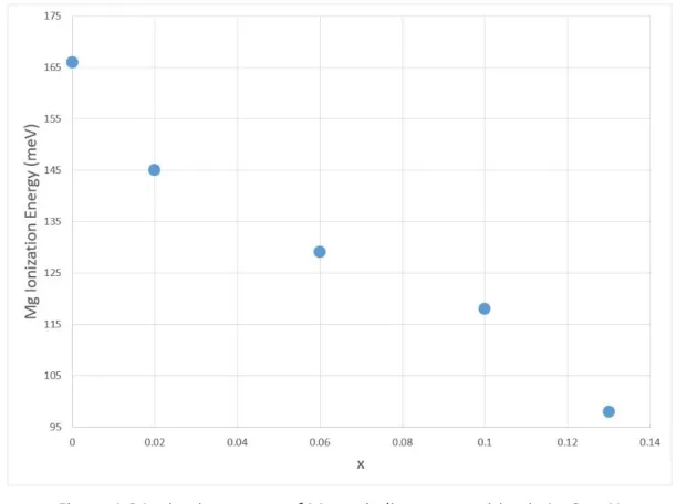
ionization energy closer to kT = 26 meV. Figure 1.3 shows the ionization energy of Mg in
InxGa1-xN plotted as a function of indium content x15. As the indium content increases, the ionization energy of Mg decreases. Although high InN% films have smaller ionization energies,
they also typically have a large background electron concentration due to poor film quality,
making p-type doping difficult.
Table 1.2 Ionization energies of III-nitride compounds as well as other relevant semiconductor compounds.
Semiconductor ED EA
InN 6.4 meV 95.9 meV
GaN 27.2 meV 204 meV
AlN 85.1 meV 1192 meV
Si 2.64 meV 6.94 meV
9 1.4 Polarization in Nitrides and QCSE
Gallium nitride exists in both the wurtzite and cubic crystalline structures. When
conventionally grown on sapphire and SiC substrates, however, the wurtzite structure is
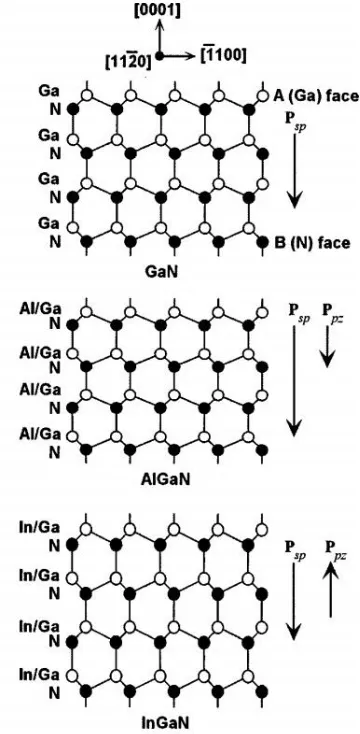
typically maintained due to a higher chemical stability16. Due to the lack of inversion symmetry in the wurtzite crystal, a net dipole moment along the c-axis is created17. Figure 1.4 a) and b) show the crystal structure and net dipole moment for Ga-polar and N-polar
crystals, respectively. The polarization charge density induces an internal electric field related
by:
𝐸𝑆𝑃 = 𝐷 𝜀⁄ − 𝑃𝑆𝑃 (1.3)
where ESP is the induced electric field, D is the displacement field, PSP is the spontaneous polarization and ε is the dielectric constant for GaN. Due to the lattice mismatch between
InN, GaN, AlN and sapphire, heterointerfaces between these materials creates crystal
stresses. The accompanying strain gives rise to piezoelectric polarization due to sheet charges
at the heterointerfaces and induces a piezoelectric electric field related by17:
10
𝐸𝑃𝑍 = 4𝜋𝑡1
𝑃1𝑃𝑍− 𝑃 2𝑃𝑍
𝑡1𝜀2+ 𝑡2𝜀1 (1.4)
where EPZ is the strain-induced electric field, PPZ1,2 are the piezoelectric polarizations, ε1,2 are the dielectric constants and t1,2 the thicknesses of layers 1 and 2, respectively. The total induced electric field of III-nitrides is simply the sum of Equations (1.3) and (1.4):
𝐸𝑖𝑛𝑑𝑢𝑐𝑒𝑑 = 𝐸𝑆𝑃 + 𝐸𝑃𝑍 (1.5)
The InxGa1-xN and AlxGa1-xN ternary alloys, when grown on GaN films, have both spontaneous and piezoelectric polarizations. Thin ternary layers grow conformally to the GaN
crystal lattice, therefore resulting in compressive and tensile stresses for InxGa1-xN and AlxGa
1-xN films, respectively. The accompanied piezoelectric field can either add (tensile) or subtract (compressive) to the spontaneous electric field, as can be seen in Figure 1.518. It has been found that although AlxGa1-xN/GaN interfaces have large discontinuities in both the spontaneous and piezoelectric polarizations, InxGa1-xN/GaN interfaces has a relatively small discontinuity in the spontaneous polarization field19. Therefore In
11
GaN/InxGa1-xN/GaN [0001] double heterostructures, which are typically used for MQW active regions, experience large internal electric fields on the order of a few MVcm-1, largely due to the piezoelectric polarization from the interfaces. These large electric fields
cause the conduction and valence bands in the InxGa1-xN quantum well to bend. The electrons in the conduction band “sit” in the lower energy states on one side of the quantum well while
the holes in the valence band “float” to the high energy states on the other side of the
quantum well. This phenomenon is called the quantum confined Stark effect (QCSE), and
12
causes two major effects to the optical properties of the quantum well. First, the change in
electron and hole energies causes a redshift (energy decrease) in the emission wavelength
that opposes the blueshift caused by the compressive strain in the quantum well. Second,
which is indeed more important, is that a spatial separation in the electron and hole wave
functions develops. This separation causes a decrease in the electron and hole wave function
overlap, thus reducing the probability of recombination, which is essential to photon
emission20. This puts an upper limit to the quantum well width as thicker wells will not emit as efficiently as thinner wells. Figure 1.6 illustrates the effect that QCSE has on quantum well
band structure, electron/hole wave function overlap and emission energy21.
13 1.5 References
1ULM University, “Bandgap-lattice constant diagram,”
http://www-opto.e-technik.uni-ulm.de/lehre/cs/III_V_map_a.jpg
2 G. Yu, Properties of Advanced Semiconductor Materials GaN, AlN, InN, BN, SiC, SiGe (John Wiley &
Sons, Inc., New York, 2001).
3 Y.N. Xu, W.Y. Ching, Phys Rev. B 48, 4335 (1993).
4 S. Nakamura, M. Senoh, N. Iwasa, S. Nagahama, Jpn. J. Appl. Phys. 34, L797 (1995).
5 S. Nakamura, Mat. Res. Soc. Symp. Proc. 482, 1145 (1998).
6 S. Nakamura, pn. J. Appl. Phys. 30, L1705 (1991).
7 J. Jasinski, Phys. Stat. Sol. (C) 2, 994 (2005).
8 T. Taliercio, P. Lefebvre, M. Gallart, A. Morel, Phys.: Condens. Matter 13, 7027 (2001).
9 K. Fujito, S. Kubo, H. Nagaoka, T. Mochizuki, H. Namita, S. Nagao, J. Cryst. Growth 311, 3011 (2009).
10 R. Dwilinski, A. Wysmolek, J. Baranowski, M. Kaminska, R. Doradzinski, J. Garczynski, L.
Sierzputowski, H. Jacobs, XXIV Int. School on Phys. Of Semicon. Comp. 88, 833 (1995).
11 R. Schlesser, Z. Sitar, J. Cryst. Growth 234, 349 (2002).
12 S.M. Bedair, F.G. McIntosh, J.C. Roberts, E.L. Piner, K.S. Boutros, N.A. El-Masry, J. Cryst. Growth
178, 32 (1997).
13 E.L. Pinder, M.K. Behbehani, N.A. El-Masry, F.G. McIntosh, J.C. Roberts, K.S. Boutros, S.M. Bedair,
Appl. Phys. Lett. 70, 461 (1997).
14 S.M. Sze, Physics of Semiconductor Devices, second edition (John Wiley and Sons, New York,
1981).
15 T. Makimoto, K. Kumakura, N. Kobayashi, J. Appl. Phys. 93, 3370 (2003).
16 H.M. Ng, N.G. Weimann, A. Chowdhury, J. Appl. Phys. 94, 650 (2003).
17 V. Fiorentini, F. Bernardini, F. Della Sala, A. Di Carlo, P. Lugli, Phys. Rev. B 60, 8849 (1999).
18 E.T. Yu, X.Z. Dang, P.M. Asbeck, S.S. Lau, J. Vac, Sci. & Tech. 17, 1742 (1999).
19 F. Bernardini, V. Fiorentini, Phys. Stat. Sol. (b) 216, 391 (1999).
20 J.S. Im, H. Kollmer, J. Off, A. Sohmer, F. Scholz, A. Hangleiter, Phys. Rev. B 57, R9435 (1998).
21 P. Waltereit, O. Brandt, A. Trampert, H.T. Grahn, J. Menniger, M. Ramsteiner, M. Reiche, K.H.
14
Chapter 2:MOCVD System and GaN Growth, Fabrication and Characterization
2.1 Introduction
In this chapter, the metal-organic chemical vapor deposition (MOCVD) system is
detailed as well as the growth process for GaN thin films. This is then followed by a
description of the fabrication techniques used to create LED devices, including
photolithography and metallization. Finally, methods of sample and device characterization
are explored with regard to III-nitride film growth and devices.
2.2 Description of the MOCVD System
For MOCVD growth, deposition occurs via chemical reactions at the substrate
surface controlled by both thermodynamics and surface chemistry. A MOCVD system can be
broken down into two parts: the gas delivery system and the reaction chamber. The gas
delivery system is used to meter the flows of reactants into the chamber, therefore
controlling the surface chemistry of the substrate. The reaction chamber houses a susceptor
on which the substrate sits, where the thermodynamics of the growth is controlled via
susceptor temperature control. Reaction byproducts are vented into the building exhaust
stack using a vacuum pump. Figure 2.1 a) and b) show a photo of the MOCVD reaction
chamber as well as schematic diagram of the system.
The reaction chamber is comprised of a custom double wall, water-cooled quartz
reactor with double o-ring seals to stainless steel top and bottom plates. The double o-ring
seal is water-cooled and evacuated using a diaphragm pump to limit oxygen diffusion into
15
shower head in order to reduce head-room and a curtain flow of either N2 or H2 is used in the shower head in order to keep reactant flow centered onto the substrate. The substrate
sits just below the shower head on a TaC susceptor, which is inductively heated using a
copper induction coil and a Lepel 7.5 kW RF power supply. A constant flow of purified N2 is maintained in the reactor to prevent oxygen and other impurities to enter the system.
As can be seen in Figure 2.1 b), our reactor utilizes a bi-channel inlet tube that
separates the column III and column V precursors until just above the susceptor. This
separation is designed to minimize gas phase reactions (especially for TMAl and CP2Mg) from occurring before the gases reach the substrate. There is, however, a tradeoff to this
kind of design. Although III and V column gas pre-mixing leads to solid phase precipitation
from the gas phase before reaching the susceptor surface, too little pre-mixing can reduce
the uniformity of reactants on the growth surface, therefore affecting sample quality. It was
16
empirically determined by others in the group that about 2 inches of vertical gas mixing is
required for optimal growth1.
The gas delivery system is comprised of two separated run/vent manifolds made of a
series of pneumatic injection valves. A schematic of the III-column run/vent manifold is
shown in Figure 2.2. Gas inputs are diverted either into the run (chamber) or vent (directly
to pump) lines so that rapid gas switching can be achieved. This design is essential when
growing heterojunctions, as the gas stream from a previous layer becomes an “impurity” of
sorts in other layers. All metal-organics (TMGa, TEGa, TMIn, TMAl and CP2Mg) are fed into the III-column run/vent manifold as well as N2 and H2 push and carrier gasses. The V-column also utilizes a run/vent manifold similar to Figure 2.2 in order to rapidly switch the V-column
nitrogen, hydrogen, ammonia and silane.
2.3 GaN Growth Procedure
GaN growth by MOCVD has been described as both an art and a science. Due to the
lack of lattice-matched substrates, GaN heteroepitaxy on foreign substrates typically
involves multiple substrate pre-treatment and conditioning steps in order to achieve high
17
quality films. This is compounded by the fact that changing one step during growth can
affect subsequent steps in different ways, therefore confounding results. This has led to a
variety of growth recipes that different groups use using processes that are still not
completely understood.
In our lab, growth of GaN thein films are done on double-side polished (0001)
sapphire substrates. Sample preparation starts with cleaving the 2” sapphire wafers into
14x14 mm samples using a diamond scribe, after which they are cleaned in
hexane/acetone/isopropanol/methanol (HAIM) for 10 minutes in an ultrasonic bath. They
are then boiled in methanol for a further 10 minutes and dried with N2 before being loaded into the reactor. The reactor is cycle purged between 15-100 torr with purified nitrogen in
order to remove chamber oxygen and moisture that might have accumulated during sample
loading.
MOCVD growth of GaN/sapphire templates is carried out by the following five steps:
1. Clean bake/substrate cleaning
2. Nitridation
3. GaN buffer layer growth
4. Buffer layer annealing
5. GaN epitaxy
First, the sapphire substate and susceptor are heated to a very high temperature
(1050 – 1100 °C) for ~20 minutes under H2 at 100 torr in order to clean the
18
thought to reduce the sapphire surface and create residual H2O, leaving behind an Al-rich sapphire surface2.
The reactor is then brought up to 350 torr and ammonia (NH3) is introduced into the V-column, starting the “nitridation” step. This step is intended to create a rough AlN surface
on the sapphire substrate which will aid in the nucleation and wetting of the subsequent
GaN buffer layer3. Many different nitridation recpies can be found in the literature; for this reactor, 5 minutes of 1.25 L/min NH3 at 975 – 1000 °C was found to be optimal.
After nitridation, the temperature is then lowered to 450-525 °C in order to grow
the GaN buffer layer. This is the most crucial step in obtaining high quality GaN epitaxy, and
is therefore monitored the closest. Changes in buffer layer temperature, thickness, growth
rate and V/III ratio can all affect the overall structural and electrical properties of the
subsequent GaN epilayer. Low growth temperature is necessary in order to grow a high
density of small cubic/wurtzite GaN islands on the nitridated sapphire surface. These islands
have been shown to enhance the reaction of pure edge dislocations with Shockley partial
dislocations, therefore leading to dislocation annihilation4. Buffer layer thickness is typically 20-50 nm thick using 1.5 cc/min of TMGa and 1.25 L/min of NH3.
The GaN buffer layer is then annealed as the reactor temperature is ramped up from
the ~500 °C buffer layer growth temperature to the ~1020 °C GaN epilayer temperature.
With a very large nitrogen overpressure (in order to minimize GaN desorption), the GaN
buffer layer undergoes a transformation from rough, highly-faceted cubic GaN to a
19
essential as the GaN epilayer must be grown on a wurtzite crystal in order to minimize
overall defect density.
Finally, the GaN epilayer is deposited on the annealed GaN buffer layer at 1000 –
1050 °C. The growth rate (as well as V/III ratio) is controlled by varying the TMGa flux. A
typical growth rate of 1.25 μm/hour was obtained with TMGa flux of 3.25 cc/min. Careful
consideration of the growth temperature, V/III ratio and H2/TMGa ratio was taken because these parameters can affect the background doping levels in GaN films. Impurities (such as
oxygen and carbon) and native defects are well-known to create n-type GaN films, so the
background electron concentration was kept to around 1015 cm-3 to avoid excessively conductive films6. Complete epilayer coalescence into smooth, specular GaN/sapphire templates occurs after about 0.5 μm of GaN growth. These templates are then used for
electronic device growth.
2.4 Device Fabrication
Device fabrication processing was performed in an 8’ x 8’ modular cleanroom
constructed in our laboratory. The ceiling is fitted with high-volume air blowers and HEPA
20
filters, providing a constant stream of clean air towards the exhaust at the bottom of the
cleanroom. Cleanroom equipment includes a chemical hood, Chemat Technologies KW-4A
spin coater, Karl Suss MJB 3 contact aligner (with 200 Wcm-2 mercury bulb) and a
Thermionics 3 kV electron-beam evaporator. A picture of our modular cleanroom can be
seen in Figure 2.3. Device isolation etching was performed by a PlasmaTherm RIE etcher (at
NCSU AIF). Before beginning the fabrication process, samples were cleaned with HAIM in an
ultrasonic bath.
The fabrication procedure consists of three different fabrication steps. The first step
involves isolating devices on the sample using a 400 μm x 400 μm device isolation mask in
the mask aligner and is illustrated in Figure 2.4. Device isolation steps are:
1. Dehydration bake at 120 °C for 5 minutes on a hot plate
2. Futurrex NR9-3000PY negative photoresist (PR) using the spin coater. Spin cycle is 10
seconds at 2000 rpm (even PR spread) followed by 40 seconds at 4000 rpm (to
achieve desired PR thickness of ~5 μm)
3. Soft bake of PR at 150 °C for 1 minute (to set PR)
4. Mask alignment of 400 μm x 400 μm device isolation mesas in the contact aligner,
followed by exposure with light power of 17 mWcm-2 for 6 seconds 5. Hard bake of PR at 120 °C for 1 minute
6. PR development in Futurrex RD-6 developer for 30-40 seconds
7. HCl dip for 20 seconds to remove native oxides
8. Load into e-beam evaporator and deposit 2000 Å of Ni to serve as an etch mask.
21
9. Warm acetone dip for PR and excess Ni removal
10.Device isolation via etching to the n-type buried layer in the PlasmaTherm RIE using
BCl3 plasma. Etch rates/depth were determined with a Dek-Tak profilometer 11.Removal of Ni etch mask with Ni-etchant solution (nitric/sulphuric/acetic acid mix)
After successful device isolation, the p-type and n-type metallizations are performed.
These step is very similar to the steps listed above. Key differences are:
1. During mask alignment, a ring-type n-contant mask is used and a mesa p-type
contact is used
2. Contact deposition consists of 500 Å Ni/1000 Å Au for the p-contact, and 250 Å
Ti/500 Å Al/1000 Å Au for the n-contact
3. After p-contact deposition, the sample is annealed 500 °C for 4 minutes under N2 to achieve ohmic contact to the p-type layer
4. There is no RIE etching in the n-contact and p-contact fabrication steps as this was
used solely for device isolation
A schematic of the final LED structure is shown in Figure 1.2 from the previous chapter.
22 2.5 Structural Characterization: X-ray Diffraction
There are numerous ways to characterize III-nitride films in order to determine
epitaxial film and device quality. X-ray diffraction (XRD) is a powerful, non-contact method
to determine several characteristics, such as thin film crystallinity, defect density and
thickness. XRD analysis for this work was done on a Rigaku Geigerflex D-Max diffractometer
with Cu radiation (λ = 1.54058 Å). For symmetric theta-two-theta (θ-2θ) XRD scans, only
crystal planes parallel to the diffractometer are visible for the given diffractometer angle.
This is due to the constructive interference of x-rays with the regular periodicity of atoms in
the sample. If a film is highly crystalline, only one set of planes will be parallel to the
diffractometer and x-ray reflections can be measured. If a sample is polycrystalline, the
random orientation of crystallites reflect all allowed reflections, of which one can determine
the ratios of each orientation from tabulated powder diffraction. The constructive
interference only occurs at certain angles that satisfy Bragg’s law:
𝑛𝜆 = 2𝑑𝑠𝑖𝑛(𝜃) (2.1)
where n is the order of diffraction, λ is the x-ray wavelength, d is the distance between
reflecting atomic planes and θ is the Bragg angle. Interatomic distance is related to the
Miller indices and unit cell dimonsions for GaN given by:
𝑑 = ( 1
(ℎ2+ 𝑘2+ ℎ𝑘) 4
3𝑎2 + 𝑙 2
𝑐2
)
1 2 ⁄
23
where h, k, and l are the Miller indices for a hexagonal lattice, and a and c are the lattice
constants.
θ-2θ scans are also routinely used to determine composition of the ternary alloys
InxGa1-xN and AlxGa1-xN by utilizing Vegard’s Law, where one can estimate the composition x of the ternary alloy by linear interpolation of the interplanar spacings of the binary
constituents:
𝑑𝐴𝑥𝐵1−𝑥𝐶 = 𝑥𝑑𝐴𝐶+ (1 − 𝑥)𝑑𝐵𝐶 (2.3)
where AxB1-xC is the ternary compound composed of the binary compounds AC and BC. Although useful in performing a quick determination of ternary composition, Equation (2.3)
does not take into account the strain state of the film. A film under biaxial stress will have
an out of plane lattice constant that is increased/decreased by compressive/tensile stress.
Since InGaN-on-GaN is under biaxial compression, the c-spacing is increased above the
equilibrium values and would therefore give an overestimation of the indium content. The
same can be said for AlGaN-on-GaN.
Structural quality of a crystalline sample can be determined with double-crystal XRD
rocking curves (omega scans). For a rocking curve scan, diffraction intensity measurements
are taken as the sample is rocked just above and below the Bragg angle for the reflection in
question. The overall full-width at half maximum (FWHM) of the rocking curves give insight
to the structural quality of the sample, where narrower line widths correspond with
high-quality films. When comparing line widths at different Bragg angles, one can determine the
24
𝑁𝑆𝑐𝑟𝑒𝑤/𝐸𝑑𝑔𝑒 = 𝛽𝑇𝑖𝑙𝑡/𝑇𝑤𝑖𝑠𝑡2
4.35𝑏𝑐/𝑎2 (2.4)
where NScrew/Edge denotes the density of screw/edge dislocations, βTilt/Twist are the tilt and twist spreads, and ba/c are the Burgers vectors of c and a-type dislocations, respectively.
Structural periodicity, such as MQWs, can also cause interferences effects to the
diffraction pattern of a propagating x-ray. The resulting interference pattern, known as
Pendellösung fringes, is related to the periodicity of the structure by:
2 sin(𝜃𝑛) − 2 sin(𝜃𝑝) = 𝑛𝜆
𝐿𝐵+ 𝐿𝑊 (2.5)
where n is the order of the satellite peaks, θn is the diffraction angle, θp is the Bragg angle of the zero order peak, LB is the thickness of the barrier layer and LW is the thickness of the well.
2.6 Structural Characterization: Electron Microscopy
Scanning electron microscopy (SEM) and transmission electron microscopy (TEM) are
critical tools that can be used to determine structural quality and surface morphology of thin
films. Secondary electrons, as well as other electrons such as backscattered and auger
electrons, are emitted during SEM analysis. Secondary electrons are typically low in energy
and are emitted from the first few atomic layers of the sample. A primary advantage of SEM
is that it is non-destructive, allowing imaged samples to be used for later measurements or
even fabricated into devices. In this research, SEM was primarily used to determine surface
25
TEM images are obtained by inelastic scattering of an electronic beam through a
sample. It is a destructive technique, as the sample must be thinned below the mean free
path of the incoming electrons to allow the beam to pass through the sample. TEM images
can be obtained using a variety of techniques such as bright field imaging (absorption of the
electrons in the material), diffraction contrast (discrete electron dispersion from sample
crystallinity) and phase contrast. This research primarily used TEM to determine epitaxial
layer thicknesses and growth rates.
2.7 Optical Characterization: Photoluminescence and Electroluminescence
Photoluminescence (PL) and electroluminescence (EL) are characterization tools used
to investigate light emission/absorption from a semiconductor sample. PL involves the use of
a light source with energy hv > Eg which excites electron-holes pairs (EHP) in the sample. EHP,
when generated in a direct band gap material, eventually recombine and emit a photon with
an energy representative of the band gap of the material. PL characterization is important as
it provides preliminary information about the band gap, dopant ionization energies, ternary
alloy composition, strain and defects, as well as others. PL is also advantageous as it does not
require electrical contacts or sample processing and therefore neglects effects from
metal-semiconductor junctions and current injection. Our laboratory uses (1) an Omnichrome 35
mW He-Cd laser (325 nm emission) as the excitation source, (2) a 0.5 m monochromator, (3)
a photomultipler tube and (4) a lock-in amplifier. Laser emission is directed onto the sample
surface using a set of UV mirrors and lenses and sample emission is collected by the
26
EL characterization is the capture of light emission from a sample in response to an
injection of electric current. For an LED structure, EL is the result of radiative recombination
of electrons and holes injected from the n-side and p-side of a pn-junction, respectively. EL
characterization reveals ultimate behavior of a fully fabricated LED, and therefore is more
conclusive than PL results. This technique can yield information similar to PL characterization,
but also data on internal electric field interactions and wavelength shift from Coulomb
screening. Our laboratory uses a Keithley 2430 SourceMeter for both continuous and pulsed
current injection. Light emission was collected through the sapphire substrate using a 600 μm
27 2.8 References
1 M. Reed, Light-emitting diodes and dilute magnetic semiconductors in the III-nitride materials
system, NCSU dissertation (2005).
2 G.W. Cullen, Heteroepitaxial Semiconductors for Electronic Devices, Springer New York, 35 (1978).
3 D. Wuu, W. Tseng, W. Lin, R. Horng, Superficies y Vacio 9, 26 (1999).
4 S.K. Mathis, A.E. Romanov, L.F. Chen, G.E. Beltz, W. Pompe, J.S. Speck, J. Cryst. Growth 231, 371
(2001).
5 S. Nakamura, G. Fasol, The Blue Laser Diode, Springer New York, 63-77 (1997).
6 J. Neugebauer, C.G. Van de Walle, Proc. ICPS-22 43 (1995).
7 S. Lee, A. West, A. Allerman, K. Waldrip, D. Follstaedt, P. Provencio, D. Koleske, C. Abernathy, Appl.
28
Chapter 3: In
xGa
1-xN Growth and Characterization
3.1 Introduction
Due to the band gap variation of InxGa1-xN (0.7 eV to 3.42 eV), this material system has received a lot of attention from researchers for visible optoelectronics such as LEDs1, laser diodes2 and optical detectors3. Growth of high-quality, high InN percentage In
xGa1-xN layers, however, has proven to be very difficult. Issues including necessary high equilibrium
N2 vapor pressure, lattice mismatch, epitaxial film relaxation, hydrogen incorporation suppression, alloy inhomogeneity and phase separation have restricted InxGa1-xN films to low values of x. In this chapter, the above obstacles will be detailed, including other
researchers’ methods to overcome them. The InxGa1-xN growth procedure is then described with careful consideration of the current limitations of growth. InxGa1-xN characterization techniques, such as x-ray diffraction (XRD), photoluminescence (PL) and scanning electron
microscopy (SEM), will also be discussed.
3.2 InxGa1-xN Growth Obstacles
Growth of InxGa1-xN films by MOCVD has some fundamental problems which have inhibited extensive research into InxGa1-xN films with large values of x. Arguably the largest issue is that a high equilibrium vapor pressure of nitrogen is required to suppress the
29
lower temperature dissociating nitrogen precursors exist, however, they also come with
both safety and impurity tradeoffs5,6.
InxGa1-xN film growth behaves similar to other III-nitride compounds in that they are governed by the same reaction principles of surface transport, atomic diffusion and
precursor desorption. Due to the weak InN bond, however, InxGa1-xN growth is typically carried out at relatively low temperatures of 650-800 °C. This is because the activation
energy for desorption of the In precursor Ed is low and is therefore inversely proportional to the growth temperature7. At higher temperatures, the indium desorption rate F
d can dominate the incorporation rate and lead to limited values of x in InxGa1-xN films. Growth at low temperatures, however, leads to issues in regard to the nitrogen vapor pressure
30
mentioned in the previous paragraph. Mesrine et. al.8 found low cracking efficiencies of NH 3 at growth temperatures necessary for InxGa1-xN growth. NH3 cracking efficiencies of only 2-4% can be achieved at these temperatures according to their study.
Low nitrogen equilibrium vapor pressures also leads to another consequence:
metallic indium droplet formation. Shimizu et. al. showed that increasing the indium vapor
pressure (therefore decreasing the nitrogen vapor pressure) led to metallic indium droplets
on the surface of samples9. Decreasing the growth temperature, which is typically done to increase indium incorporation, also causes indium droplet formation due to the poor
cracking of NH3. The droplets on the surface act as indium sinks, creating areas of high indium concentration at the droplets and low indium concentration in the surrounding
epitaxial layer10. Alloy inhomogeneity can cause a variety of issues for optoelectronic
31
devices, such as broad emission spectrums in LEDs and high threshold currents in LDs. If the
growth temperature is reduced even further, poor surface mobility due to entering the
kinetic growth regime can induce three-dimensional growth and very poor optical
characteristics.
Due to the 12% lattice mismatch between InN and GaN, InxGa1-xN films grown on GaN are subject to compressive stress in order to lattice match the GaN film underneath.
Typically, InxGa1-xN films are grown pseudomorphically to GaN films so that the InxGa1-xN films are coherently strained to the GaN lattice. As the thickness of the InxGa1-xN film increases, the film strain energy increases until the strain energy exceeds a critical value, in
which case the film begins to relax. This is known is the critical layer thickness (CLT). InxGa
1-xN film relaxation causes many detrimental phenomena including misfit dislocation
creation, indium inhomogeneity and three-dimensional growth. Parker et. al.11 studied the CLT of InGaN/GaN heterostructures and found the value to depend on the indium
composition of the film. Figure 3.2 shows the variation of the InxGa1-xN/GaN
heterostructure CLT with respect to indium content x. InxGa1-xN films with x < 0.06 have been extensively studied due to the large value of CLT. When the indium content increases,
however, the CLT value drops rapidly due to the increase in film strain.
The presence of atomic hydrogen also has a profound effect on the growth of InxGa
1-xN films. Typically, hydrogen is used as a carrier gas in III-nitride films as it reduces impurity densities and facilitates growth rate control through etching12,13. Piner et. al.14 found that atomic hydrogen drastically reduces the indium incorporation of InGaN films. By reducing
32
much indium for a given growth temperature. It is suggested that the hydrogen may have
an effect on the residence lifetime of the indium species at the growth surface. A lower
residency time means that the indium atom may desorb before binding with a dangling
nitrogen bond, and therefore decrease the indium incorporation.
Indium inhomogeneity in InxGa1-xN films also has limited optoelectronic device performance. Pantzas et. al.15 studied the relaxation mechanism of 0.12 < x < 0.16 In
xGa1-xN films grown by MOVPE and found that spontaneous 2D/3D transition occurs due to lateral
fluctuations in the indium composition. Figure 3.3 shows an indium content map of a 60 nm
In0.16Ga0.84N film, obtained by interpolating 200 EDX measurements from the InGaN/GaN interface to the InGaN surface. They also found that the InGaN films relax in three distinct
stages. First, the InGaN film is pseudomorphically strained to the underlying GaN layer with
very little indium fluctuation. Large fluctuations of indium then appear in the film to
compensate for the building strain. Finally, since the indium-rich regions contain a higher
element III concentration and therefore a higher growth rate, 3D growth begins. The
33
thicknesses of these three relaxation regions depend on the indium content of the InxGa1-xN film, as larger InN percentages causes strain to build quicker in the film, leading to smaller
relaxation thicknesses.
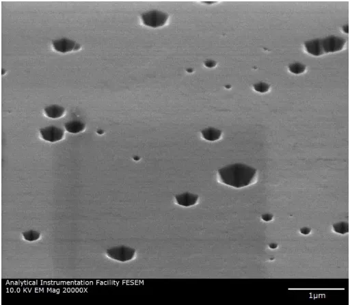
The most commonly known macroscopic defect of thick, relaxing InxGa1-xN films is known as the “V-pit” (or V-defect, V-groove, pinhole)16,17,18. V-pits are believed to initiate at threading dislocations and are characterized as an open hexagonal inverted pyramid
defined by the six {10-11} planes. Figure 3.4 shows an SEM image of the surface of a thick
InxGa1-xN layer displaying V-pitting on the surface. V-pits cause deep level emission tails in PL emission spectra due to the localization of indium at the apex and walls of the V-pit. The
V-pits initiate at the transition from 2D to 3D growth, and due to differing growth
rates/indium incorporations of the polar (0001) and semipolar {10-11} planes, exacerbate
34
this phenomenon. Threading dislocations and V-pitting in QWs have also been found to
decrease efficiency and carrier transport due to nonradiative recombination.
The interatomic spacing between InxGa1-xN layers grown on GaN also leads the compositional instability of phase separation. Many groups have found evidence of phase
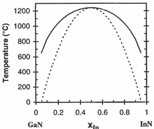
separation, which is the thermodynamic instability of strained InxGa1-xN films19,20,21. Ho and Stringfellow22 derived a theoretical model for a temperature versus x phase diagram for InxGa1-xN alloys. Figure 3.5 shows the GaN/InN phase diagram with respect to temperature. Above the binodal curve (solid line) an InGaN alloy is thermodynamically stable. This region,
however, is well above the growth temperatures necessary for InxGa1-xN growth. Below the spinodal curve (dashed line), InxGa1-xN films are thermodynamically unstable and phase
separation will occur, resulting in films with regions of high and low indium concentrations.
The gap between the curves is known as the metastable region, where phase separation is
only possible from nucleation. Typical InxGa1-xN films are grown between 650-800 °C, which
35
would put a majority of the films grown in the metastable region if the InN percentage is
greater than 0.06.
3.3 InxGa1-xN Growth Procedure
InxGa1-xN films were grown by MOCVD on GaN/sapphire templates due to the unavailability of lattice-matched substrates. First, a GaN template was carefully calibrated
and grown using the procedure detailed in Chapter 2.3. Just before the template growth has
completed, the trimethylindium (TMIn) and triethylgallium (TEGa) MO sources are
prepared. A 7:1 TMIn:TEGa molar ratio is typically held, although this ratio was intentionally
changed for a few experiments. When the GaN template has finished, the TMGa precursor
and all hydrogen flows are shut off and the reactor temperature is ramped down to the
InGaN growth temperature between 650-800 °C. After temperature stabilization, InGaN film
growth is initiated by running both the TEGa and TMIn precursors into the chamber. The
indium content in the InGaN films were controlled by changing the temperature of the film;
Figure 3.6 θ/2 θ XRD scans of a 100 nm (black curve) strained InxGa1-xN film and 200 nm (red curve) relaxed InxGa1-xN film grown on
36
hot growths led to films with low indium contents while cold films led to films with
increased indium contents. InGaN layers were typically capped with 2-5 nm of GaN to
prevent surface desorption of indium when the growth had finished.
3.4 InxGa1-xN Film Characterization
InxGa1-xN films grown on GaN/sapphire templates can be characterized by a variety of methods. XRD has become a dominant method to determine both indium content and
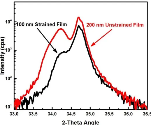
thickness of InxGa1-xN films. XRD measures the average value of the lattice constant of epitaxial layers, and since the lattice constant of InxGa1-xN is dependent on the indium composition x, an average indium content can be determined for the film. Figure 3.6 shows
XRD measurements for two InxGa1-xN films grown at 750 °C with film thicknesses of 100 and 200 nm on GaN/sapphire templates. The films are grown with an intended indium content
of x = 0.10, which puts the CLT around 120 nm according to Figure 3.2. Therefore, the 100
nm (black curve) film would correspond to strained InxGa1-xN while the 200 nm (red curve) film would correspond to strain-relaxed InxGa1-xN. The lattice constant c in the growth direction for any allowed reflection is given by Gragg’s Law:
𝑐 = 𝑙𝜆
2𝑠𝑖𝑛𝜃𝐵 (3.1)
where λ is the radiation wavelength (0.15418 nm for Cu Kα emission) and θB is the Bragg angle estimated from the peak of the XRD measurement. The large peak at 2θ = 34.6°
corresponds with the GaN lattice constant of c(GaN) = 5.1838 Å for the underlying GaN
template. The peak at 2θ = 34.3° and 2θ = 34.24° corresponds to c(InGaN) lattice constants
37
XRD peak is due to the relaxation of the InxGa1-xN film. As the thickness exceeds the CLT, the film relaxes from pseudomorphically strained InxGa1-xN to inhomogeneous, relaxed InxGa
1-xN. The lattice of the relaxed InxGa1-xN film is no longer under compressive strain, so the lattice constant increases. The average indium composition can be estimated using Vegard’s
law, which assumes a linear scale of the lattice constant from GaN to InN with respect to
the indium content:
𝑐(𝐼𝑛𝐺𝑎𝑁) = 𝑐(𝐼𝑛𝑁) + (1 − 𝑥)𝑐(𝐺𝑎𝑁) (3.2)
The indium content of these InxGa1-xN films are therefore estimated to be 0.087 and 0.102 for the 100 and 200 nm thick films, respectively. The indium content of the pseudomorphic
sample (100 nm, black curve) is underestimated due to the biaxial strain in the layer,
causing a distortion in the hexagonal unit cell.
A majority of the optical properties of InxGa1-xN films can be determined by PL. Figure 3.7 shows the room temperature PL of 100 nm strained (black curve) and 200 nm
38
relaxed (red curve) InxGa1-xN films grown at 750 °C. For the 100 nm pseudomorphically strained InxGa1-xN film, the PL emission is dominated by the band edge emission corresponding with the InxGa1-xN optical band gap. The intensity and FWHM of the PL emission are directly related to the quality of the InxGa1-xN film, with brighter/narrower emissions corresponding to higher quality films. As is typical with InxGa1-xN films grown thicker than a few nanometers, the PL emission of the strained film is also accompanied by
a deep level emission at a longer wavelength. Although the film is strained to the GaN
lattice underneath, the unfavorable conditions for InxGa1-xN growth leads to highly defective films. The 200 nm relaxed InxGa1-xN film is dominated by these deep levels, as can be seen in Figure 3.7. The formation of V-pitting on the surface as well as the indium inhomogeneity
leads to a severe decrease in the band edge emission. The indium content of the InxGa1-xN films can be estimated by using a model developed by Emara et. al23. Although this model was developed for QW emission, it can be adapted for bulk InxGa1-xN films by neglecting the shift in emission energy due to QCSE. From the model, the indium composition is estimated
to be x = 0.1.
As was seen in Figure 3.4, electron microscopy is a pivotal tool in determining the
surface morphology and thicknesses of InxGa1-xN films. SEM was used extensively to determine surface morphology of bulk InxGa1-xN films, as well as for the films to be
discussed in the next chapter. Due to the high difficulty and cost of TEM, this technique was


![Figure 3.1 Equilibrium vapor pressure of N2 over AlN, GaN and InN. From [4].](https://thumb-us.123doks.com/thumbv2/123dok_us/1408089.1173418/43.612.200.432.71.398/figure-equilibrium-vapor-pressure-over-aln-gan-from.webp)
![Figure 3.2 Variation of InxGa1-xN/GaN heterostructure CLT with indium content x. From [11]](https://thumb-us.123doks.com/thumbv2/123dok_us/1408089.1173418/44.612.202.430.74.365/figure-variation-inxga-gan-heterostructure-clt-indium-content.webp)