IJEDR1402037
International Journal of Engineering Development and Research (www.ijedr.org)1514
Abstract—Design and implementation of process resilient multiple phase clock generator plays a major role in lots of applications over in communication and signal processing arena. we are planning to design a highly efficient multiple phase clock generator. The configurable platform utilizes logics efficiently and perform the required functions for various applications. If certain part of the function is required we can simply configure the bits and we implement the design. The repeatable, self healing technique adopts the signals to be generated in a constant manner , and the per phase delay is being reduced than 100ps.The application using the shifted clocks also developed here, we propose a cymmometer system where the unknown frequency is determined by using the standard frequencies and the phase shifted clocks are applied over here for range determinationI.INTRODUCTION
IJEDR1402037
International Journal of Engineering Development and Research (www.ijedr.org)1515
The methodology to be presented in this brief has a simpler architecture. Also, it uses only standard cells and thus can lend itself to automation in the future.II.PRELIMINARIES
More formally, the MPCG problem is to design a circuit that can generate a sequence of clock signals {φ0,φ1, . . . , φN }. The parameter N is used to represent the total number of phases. In some cases, it is as small as just 2. But in some other cases, it could be a larger number, say 16 as in our Radar SoC. The multiphase clock signals have the same frequency, denoted as F, while their clock cycle time (or clock period) is denoted as T . Next, we will define some related terminologies more formally, so as to make our presentation more clear.
Definition 1: The rising edges of every two consecutive clock signals, e.g., {φi and φi+1}, are apart by a fixed timing interval, referred to as per-phase delay, denoted as δnotch. For simplicity
without losing generality, we assume that the clock period is equal to N times the per-phase delay, i.e., T = N × δnotch. In some sense, a clock period is now divided into N notches evenly. This assumption leads to a phenomenon that the clock signal of the last phase (φN ) ought to be edge-aligned with the clock signal of the initial phase (φ0).
Definition 2: Relative phase or simply phase of a clock signal is referred to the relative timing position of the rising edge of a clock signal as compared to that of φ0 (which is considered as a reference clock signal). Based on this definition, we will say that the phase of φ0 is zero, and the phase of φi is i × δnotch.
Definition 3: Two clock signals, say {φx , φy}, are denoted by φx ≡ φy , if their phases are the same. Sometimes, we also depict that these two signals are in-phase or edge-aligned, and use these phrases interchangeably.
1) Cyclic Property of a Clock Signal’s Phase: In general, a phase is a concept similar to the time delay except that the phase is cyclic. That is, for a phase larger than a reference period, say T , we can modulo T to derive its equivalent phase
Equivalent − Phase = Original_Phase % T.
This property is based on the observation that the Waveform of a clock signal with a phase of ―p‖ and the waveform of a clock signal with a phase of ―p plus a number of clock periods‖ do not have any ifference in their waveforms. By applying the above modulo operation, we can confine the phase of a clock signal to [0, T ].
Definition 4: We define the phasor plot of a MPCG problem, as
IJEDR1402037
International Journal of Engineering Development and Research (www.ijedr.org)1516
III.INTRODUCTION TO MPCG
A. Basic Cyclic MPCG Architecture
IJEDR1402037
International Journal of Engineering Development and Research (www.ijedr.org)1517
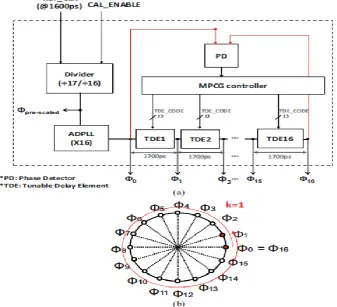
In Fig. 4, we show an example of using k = 1, in which the desired delay across each TDE is (1 × 1600 + 100) = 1700 ps. On the phasor plot as shown in Fig. 4(b), the clock signal produced by TDE1, denoted as φ1, travels the entire circle once and then settles down to the correct positionB. TDE
The proposed TDE is shown in Fig. 5. To minimize the variation of the duty cycle when a clock signal passes through the delay path, we use a pair of the delay stages, which are composed of inverters, one labeled as odd delay stage and the other is labeled as even delay stage. When one clock signal passes through the odd delay stage, the pulse width of the clock signal will be inversed and modified (in a way of being either shrunk or sometimes expanded). However, the inversed modified pulse can be recovered when passing through the even delay stage. Overall, the duty cycle is almost invariant through the two delay stages combined. The resolution of the TDE used in proposed architecture is mainly dictated by the two-input NAND gates used as variable loading proposed in at the outputs of the multiplexers. The delay across a delay stage can now be finely tuned by controlling a (M + 1)-bit thermometer γ -code, with each bit of this code controlling the sideinput of a NAND gate. This is due to the fact that each extra turned-on NAND gates will cause a slight change on the loading effect at the output node it connects to. The tuning resolution of a TDE is about 3.14 ps in a typical 0.18-μm CMOS process, while it can be improved to 1.91 ps in a 90-nm CMOS process.
IV.PROCESS CALIBRATION
IJEDR1402037
International Journal of Engineering Development and Research (www.ijedr.org)1518
1) we relax the stringent requirement of the TDE, and 2) we find a way to control each of them separately but precisely.A. Process-Resilient Architecture
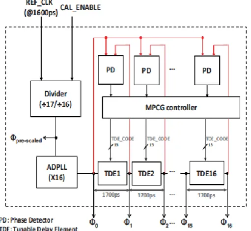
Fig. 6 depicts the architecture of a cyclic MPCG design that can adapt to the true silicon speed of a manufactured chip and make the delay of each TDE equal as much as possible. In addition to the original chain of TDEs, the distinctive feature added is the incorporation of an all-digital phase-locked loop (ADPLL) responsible for generating the calibration clock signals. The following paragraph describes our basic idea. Unlike the traditional MPCG design, we need to precisely control the edge position of not just the final phase of clock signal, φ16, but also every internal phase of clock signal, i.e., {φ1, φ2, . . . , φ16}. This may seem quite challenging, but indeed achievable since the delay of each TDE has been much larger after we have applied the cyclic property. In practice, this can be done by adjusting the frequency (or the clock period in other words) of the input clock signal φ0. For example, if we adjust the clock period in our working example from the original 1600 to 1700 ps, then the goal of process calibration is to make all phases of clock signals in-phase with φ0 in our cyclic MPCG design. If this criterion is achieved, then we will have successfully placed the edge position of each phase of clock signal at its right timing location within a very small error range roughly determined by the tuning resolution of a TDE.
The modified architecture operates in two different modes: 1) the process calibration mode after power up, and 2) the functional mode. These two operational modes accept a reference clock signal of different frequencies (or clock periods). In our working example, the clock period is 1700 ps in the calibration mode, whereas 1600 ps in the functional mode. These two requirements can be integrated as an ADPLL, explained below.
1. The input is an external clock signal, denoted as φref , with the functional clock period (e.g., 1600 ps in our example). 2. There is a frequency divider (as a pre-scaler) that divides the frequency of φref by (N +1) in the calibration mode, and N
in the functional mode. In terms of clock period, this is equivalent to stretching φref by (N + 1) or N times, producing a clock signal called φpre−scaled
3. The basic function of the ADPLL is to multiply the frequency of clock signal φpre−scaled by a multiplicative factor equaling the number of phases, N, and N = 16 in our example. In terms of clock period, φpre−scaled is shrunk by N times when producing clock signal φ0.
IJEDR1402037
International Journal of Engineering Development and Research (www.ijedr.org)1519
B. Process Calibration ProcedureAfter powering up, our MPCG design will go through a calibration procedure before getting ready for the normal operation. Basically it first sets up the ADPLL to produce a calibration-purpose clock signal φpre−scaled (with the clock period one notch higher than the target one) and then decides the tuning code for each TDE, one at a time, following the order from φ1 to φ2, and all the way to φ16. As previously mentioned, all these phases of clock signal should be edge-aligned with φ0 during the calibration mode. Once the calibration is done, a nominal tuning code has been set to each TDE. Typically, deciding a tuning code for a TDE is itself a mini-search process. After that, we switch the MPCG design to the functional mode, in which the clock period of φ0 returns to the functional one, say 1600 ps in our example
C. Dynamic Tracking
During the normal operation, we still need to adjust the tuning code of each TDE slightly to make it adaptive to potential supply voltage or temperature variation. Note that at the moment there is no way to align the internal clock signals {φ1, φ2, . . . ,φ15}. We can judge by the phase of the final output clock signal, φ15, by comparing it to the initial clock signal φ0. We change the turning codes of the TDEs based on phase comparison results. Since we are in a phasemaintenance stage, we will increment or decrement the fine-tuning code of only one TDE at a time to minimize the amount of phase change, albeit in a round robin order. That is, each TDE must be tuned in turn.
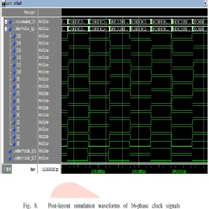
V.EXPERIMENTAL RESULTS
IJEDR1402037
International Journal of Engineering Development and Research (www.ijedr.org)1521
Standard cell library to improve the accuracy, or 2) we can simply use a more advanced process, if that is available. For example, the phase error in our design can be reduced from 11 ps to only 4 ps after shifting from a 0.18 μm process to a 90 nm process. The power consumptions of our 4-phase clock generator design are 22.9 mW for 0.18 μm process and 3.4 mW for 90 nm process, respectively. In terms of power consumption, the work in is 81/22.9 = 3.53 × that of ours. It is also notable that the work in consumes only 18 mW. This is partly due to its low operating frequency at 150 MHz. After scaled by the supply voltage factor (1.82/3.3)2 and the clock frequency factor (2000 MHz/150 MHz), the power consumption in will translate to roughly 71 mW, which is still (71/22.9) = 3.1 × that of our version in the 0.18 μm processVI.CONCLUSION
When it comes to the design of a MPCG, the selected process technology may impose some limitations that do not seem to be reconcilable by standard cells—e.g., the amount of small delays one wish to control precisely across a delay cell. One may choose to use pricer and more advanced processes to alleviate this problem, but the process variation still may make process calibration necessary. In this brief, we have found that we can actually boost the performance of a MPCG design tremendously via architectural innovations. The design was robust (even for advanced processes) and highly accurate with small phase errors. Even better, it lent itself to automation since it only used standard cells. Post-layout simulation validated that this method can achieve much smaller area and power consumption than previous works. We also used this method to asily generate a 16-phase MPCG design meeting the requirement of an in-house radar SoC design using just 0.18-μm CMOS process technology.
REFERENCES
[1] C.-C. Chung and C.-Y. Lee, ―A new DLL-based approach for all-digital multiphase clock generation,‖ IEEE J. Solid-State Circuits, vol. 39, no. 3, pp. 469–475, Mar. 2004.
[2] C.-C. Chen, J.-Y. Chang, and S.-I. Liu, ―A DLL-based variable-phase clock buffer,‖ IEEE Trans. Circuits Syst. II, Exp. Briefs, vol. 54, no. 12, pp. 1072–1076, Dec. 2007.
[3] C.-N. Chuang and S.-I. Liu, ―A 0.5–5-GHz wide-range multiphase DLL with a calibrated charge pump,‖ IEEE Trans. Circuits Syst. II, Exp. Briefs, vol. 54, no. 11, pp. 939–943, Nov. 2007.
[4] C.-N. Chuang and S.-I. Liu, ―A 20-MHz to 3-GHz wide-range multiphase delay-locked loop,‖ IEEE Trans. Circuits Syst. II, Exp. Briefs, vol. 56, no. 11, pp. 850–854, Nov. 2009.