A Compact UWB Band Pass Filter Using Simple Defected
Ground Structures
Ali Mokhtarani and Arash Ahmadi*
Abstract—In this paper an ultra-wideband band (UWB) pass filter is introduced. The filter is composed of multiple shorted shunt stubs and some defected ground structures (DGS). The defected ground structures are composed of some circular-shape defects and diagonal-line patterns. The bend-shaped defected-ground structure is thoroughly studied and compared to some other defected structures. The filter features a simple structure and small dimensions (12×22 mm2). Meanwhile, a systematic design method is presented. The analysis method is based on numerical methods and is verified by a commercially available EM simulator. The 3 dB passband of the proposed wide band filter is between 2 GHz and 10 GHz.
1. INTRODUCTION
Microwave filters play a major role in telecommunication systems. There are major trends to reduce the dimension and improve the frequency response of the microstrip filters. Microstrip filters are planar circuits that can be easily integrated with other electronic circuits and components, and feature small dimensions. Microstrip band-pass filters suffer from higher frequency resonances and passbands due to the distributed effects. To suppress the unwanted passbands of a band-pass filter, some low-pass filters must be cascaded with the band-pass filter. As a consequence, the overall dimension of the filter increases. Defected ground structures have been used in microwave circuits and antennas for shaping the frequency response and improving the out of band performance [1, 2]. The addition of a DGS to a microwave filter improves the out of band rejection property of the filter without increasing the dimensions. In some cases the in band frequency response of the filter is affected too, and the net effect is an overall size reduction. A Low-pass and a band-pass filter with an H-shaped defected-ground structure have been introduced in [1]. The effect of a fractional pattern in the ground plane was studied in [2]. In both cases the frequency response of the filters was shaped through the DGS and major improvements observed. A DGS can be a simple cut in the ground plane or a void in the ground plane with the shape of an H or a dumbbell [3]. Although more complex patters can be used as a DGS, the analysis and design of these patters become complex [2, 4–6]. Not only does the out of band rejection of a microstrip filter improve through the presence of a DGS, the maximum frequency of the rejection band of a microstrip filter also increases as demonstrated in [7].
In this work several circular-shaped DGSs have been used to improve the frequency response of a band-pass filter. The analytical formulas, presented in the following sections, simplify the calculation of the resonant frequency introduces by a DGS.
2. THE DGS
The DGS is, in fact, a discontinuity or a cut in the ground plane of a microstrip line or microstrip circuit. The DGS affects the path of the current in the ground plane. The net effect is a resonant
Received 20 November 2017, Accepted 28 June 2018, Scheduled 29 September 2018
* Corresponding author: Arash Ahmadi ([email protected]).
circuit in series with the primary microstrip line or circuit. In many applications the DGS is modeled by a parallel RLC resonator which is connected in series with the circuit. The parallel RLC resonator introduces transmission zeros in the transfer function of the circuit. A defected structure is simple to integrate with a planar circuit as microstrip filters and affects the frequency response of the circuit.
A diagonal cut in the ground plane of microstrip line is shown in Fig. 1. This is one of the easiest defected-ground structures. The discontinuity in the ground plane introduces a transmission zero for the current at DC and at a frequency, known as the resonance frequency of the circuit. For this reason the DGS is modeled as a parallel RLC resonator in series with a DC blocking capacitor. The value of this capacitor depends on the width of the gap and length of the cut in the ground plane.
(a) (b)
Figure 1. (a) A transmission line and a cut in the ground plane as a DGS. (b) The equivalent circuit of the DGS.
There are other types of DGS where some forms of defects in the ground plane are used to introduce a resonant circuit in the frequency response of the circuit. Fig. 2 shows some other shapes of DGSs. The transmission zero at DC disappears in these structures because of the finite dimension of the defects in the ground plane. These DGSs have the equivalent circuit of a parallel resonant RLC circuit (without the series capacitorC2) in series with the transmission line.
(a) (b) (c) (d)
Figure 2. (a) Circular-shape DGS (type 1). (b) Broken-line DGS (type 2). (c) Straight-line DGS (type 3). (d) The equivalent circuit of three defected-ground structures.
The DGS in Fig. 2(a) is an open ring shaped cut in the ground plane of a microstrip line, and K is the spacing between the open ring ends. The DGSs in Figs. 2(b) and (c) are diagonal and straight cuts in the ground plane, respectively. The equivalent circuit of these defected ground structures is shown in Fig. 2(d).
These circuits are simulated in HFSS, which is a full wave simulator. The dimensions of the defects are such that a transmission zero results at 14.5 GHz. The frequency response of these DGSs are simulated and compared in Fig. 3.
Figure 3. Simulated scattering parameters of three types of defected ground structures.
circuit to the simulation results. TheS parameters of a DGS can be obtained with the aid of a full wave simulator as HFSS. The equivalent circuit parameters of the three DGSs of Fig. 2 have been derived by the fitting method. In the case of a defect of straight-line shape, R1 = 986 Ω, L1 = 0.591 nH and
C1 = 0.203 pF. In the case of a V-shape cut in the ground plane, R1 = 1412 Ω, L1 = 0.477 nH and
C1 = 0.251 pF. In the case of a defect in the ground plane of the semi-circular shape, R1 = 2273 Ω,
L1 = 0.269 nH and C1 = 0.445 pF.
Comparing the frequency response of the three DGSs, the semi-circular cut in the ground plane has the highest quality factor for the same magnitude of transmission zero. The resonance frequency for the defected circular DGS with a spacing ofK between the ring ends, as shown in Fig. 2(a), can be derived by calculating at first the arc length of the ring as:
L= 2R (
π−sin−1
( K
2R ))
(1)
where R is the radius of the ring. The resonant frequency of the ring is at a frequency, where the arc length equals one wavelength. For this reason the resonance frequency is
fresonance=
c L√εr
(2)
wherec is the speed of light, andεr is the dielectric constant of the substrate. The open ring is placed in the ground plane of the microstrip line. The speed of the wave and the wavelength are not easy to calculate analytically. An empirical fitting parameter is used to correct Eq. (2), and the corrected resonant frequency is given in Eq. (3).
fresonance=
λc (
(√εr) 2R (
π−sin−1
( K
2R
))) (3)
where λ = 338, and it is the empirical parameter. It has been obtained by simulating multiple semi-circular DGSs with different values of R and resonance frequencies. This method is valid for small values ofK. Throughout this paper the opening of the rings is taken to be 1 mm.
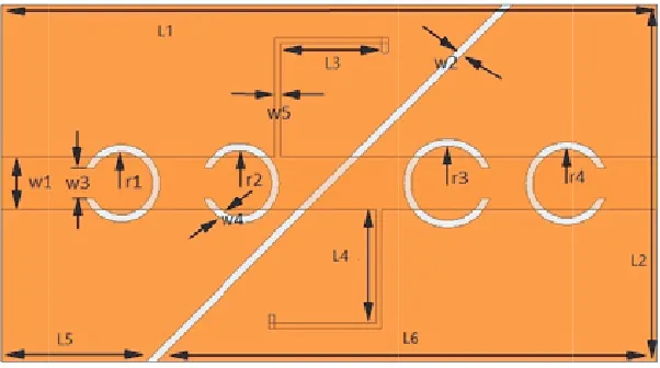
3. DESIGNING THE UWB BAND PASS FILTER
Figure 4. The layout of the proposed bandpass filter.
Figure 5. The band pass filter modeled by several sub components.
To compute the frequency response of the filter, each component in the layout is modeled as a block. These blocks are cascaded as shown in Fig. 5 and are connected by some 50 Ω transmission lines. The ABCDmatrix of each sub-component can be obtained by several methods.
It is worth noting that the dimensions of stubs and each DGS are unknown and must be obtained according to the desired overall frequency response.
TheABCD matrix of the interconnecting 50 Ohms transmission line of length l is [10]
A=
[
cosh ((α+iβ)l) 50 sinh ((α+iβ)l) 1
50sinh ((α+iβ)l) cosh ((α+iβ)l)
]
(4)
whereα and β are the attenuation and propagation constant of the transmission line, respectively. The DGS and shorted shunt-stub are modelled as two port networks with the ABCD matrices given in Eqs. (4) and (6), respectively.
A1 =
[
1 ZDGS
0 1
]
(5)
A2 =
[
1 0
Ystub 1
]
(6)
where ZDGS and Ystub are the equivalent series impedance of the DGS and parallel admittance of the shorted shunt stub, respectively. The corresponding expressions are given in Eqs. (7) and (8).
ZDGS = R+ 1
jωC +jωL (7)
where R, C and L are the equivalent circuit parameters of the DGS. Y0 and θ are the characteristic admittance and electrical length of the shorted stub, respectively.
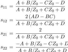
The ABCD matrix of the entire circuit is equal to the product of the ABCD matrices of the individual sub-components. The proposed filter consists of fourteen different sub-circuits. The scattering parameters of the complete filter are computed from the elements of the overall ABCD matrix using the following relations [10].
s11 = A+B/Z0−CZ0−D
A+B/Z0+CZ0+D
(9)
s12 =
2 (AD−BC)
A+B/Z0+CZ0+D
(10)
s21 =
2
A+B/Z0+CZ0+D
(11)
s22 = −
A+B/Z0−CZ0+D
A+B/Z0+CZ0+D
(12)
4. MEASUREMENT AND SIMULATION RESULTS
The band-pass filter is synthesized from a pure all pass transmission line. The passband and out-of-band rejection of the filter are shaped by insertion of some transmission zeros. The DGSs and shorted stubs are responsible for these transmission zeros. The frequency of the transmission zeros is dependent on the passband and the desired out-of-band rejection. The transmission zeros can be deliberately distributed over the rejection band of the filter, and there is not a unique method for this type of design. The resonance frequency of each sub-circuit that comprises the band-pass filter is given in Table 1. A transmission zero is added in the frequency response of the filter due to each resonance frequency.
Table 1. The resonance frequency of each sub circuit.
Sub circuit Resonance frequency (transmission zero)
Semi circular DGS withR= 1.05 mm 16 GHz
Semi circular DGS withR = 1.1 mm 15.3 GHz
Semi circular DGS withR= 1.25 mm 13.3 GHz
Semi circular DGS withR= 1.15 mm 14.5 GHz
Shorted stub DC and 12.1 GHz
Cut in the ground plane DC and 12.85 GHz
With the aid of a computer optimization in Matlab using the constraint that the passband should be within 2 GHz and 10 GHz, the unknown parameters will be determined. The unknown parameters that are determined are the characteristic impedances of the DGS and shorted stubs and the length of the interconnecting transmission lines.
Finally, a UWB band-pass filter with a passband of 8 GHz has been designed. The frequency of the transfer zeros are controlled by the DGSs. The 50 Ω transmission lines and shorted stubs help to match the input and output of each DGS to the rest of the circuit. The dimensions of the filter are listed in Table 2.
Table 2. The dimensions of the filter obtained by computer optimization.
W1 W2 W3 W4 W5 L1 L2 L3
1.8 mm 0.25 mm 1 mm 0.25 mm 0.2 mm 22 mm 12 mm 3.6 mm
L4 L5 L6 R1 R2 R3 R4
3.8 mm 4.8 mm 16.6 mm 1.05 mm 1.1 mm 1.25 mm 1.15 mm
(a) (b)
Figure 6. Photograph of the proposed filter. (a) Top view. (b) Bottom view.
Figure 7 shows the measured S parameters of the wide band filter. Computer simulations using Matlab are compared with the measurements and simulation results of HFSS, which is a full wave simulator.
Figure 7. Measured and simulated frequency response.
effects as high frequency resonances and inter coupling. That is the reason for the discrepancy between the simulation and measurements in the out-of-band response.
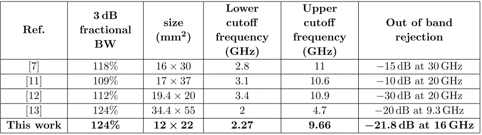
The measured fractional bandwidth (FBW) of the filter is approximately 124% and is more than two octaves wide. In Table 3, the performances of the proposed filter and some other UWB filters are compared.
Table 3. The performance comparison of the proposed UWB filter.
Ref.
3 dB fractional
BW
size (mm2)
Lower cutoff frequency (GHz) Upper cutoff frequency (GHz)
Out of band rejection
[7] 118% 16×30 2.8 11 −15 dB at 30 GHz
[11] 109% 17×37 3.1 10.6 −10 dB at 20 GHz
[12] 112% 19.4×20 3.4 10.9 −30 dB at 20 GHz
[13] 124% 34.4×55 2 4.7 −20 dB at 9.3 GHz
This work 124% 12×22 2.27 9.66 −21.8 dB at 16 GHz
5. CONCLUSION
In this paper a wideband, band-pass filter, with small dimensions has been introduced, which uses the response shaping properties of simple DGSs. The effect of the line bending in the shape of the defected-ground structure was investigated for three simple structures, and an empirical formula was presented that can predict the resonance frequency of the defected circular structures. The measured 3-dB fractional bandwidth is 124% compared to 146% obtained by simulation. The results obtained by measurements and simulations are in acceptable agreement. A UWB filter incorporating some DGSs can be modeled by cascaded connection of some DGSs.
REFERENCES
1. Boutejdar, A., A. Omar, E. P. Burte, and R. Mikuta, “An improvement of defected ground structure lowpass/bandpass filters using H-slot resonators and coupling matrix method,”J. Microw.
Optoelectron. Electromagn., Vol. 10, No. 2, 295–307, 2011.
2. Kufa, M. and Z. Raida, “Lowpass filter with reduced fractal defected ground structure,”Electronics
Letters, Vol. 49, No. 3, 199–201, 2013.
3. Abdel-Rahman, A. B., A. K. Verma, A. Boutejdar, and A. S. Omar, “Control of bandstop response of hi-lo microstrip low-pass filter using slot in ground plane,” IEEE Trans. Microw. Theory Tech., Vol. 52, No. 3, 1008–1013, 2004.
4. Song, K., Y. Z. Yin, X. Yang, J. Y. Deng, and H. H. Xie, “Compact LPF with pair of coupling slots for wide stopband suppression,”Electronics Letters, Vol. 46, No. 13, 922–924, 2010.
5. Ting, S. M., K. W. Tam, and R. P. Martins, “Miniaturized microstrip lowpass filter with wide stopband using double equilateral U-shaped defected ground structure,” IEEE Microwave and
Wireless Components Letters, Vol. 16, No. 5, 240–242, 2006.
6. Mou, J., Y. Weihua, and L. Xin, “Compact ultra wideband bandpass filter based on novel defected ground structure and folded coupled lines,” Microwave and Optical Technology Letters, Vol. 53, No. 7, 1598–1601, 2011.
8. Abdel-Rahman, A., A. R. Ali, S. Amari, and A. S. Omar, “Compact bandpass filters using defected ground structure (DGS) coupled resonators,”2005 IEEE MTT-S International Microwave
Symposium Digest, 1479–1482, Long Beach, CA, June 2005.
9. Woo, D.-J., T.-K. Lee, J.-W. Lee, C.-S. Pyo., and W.-K. Choi, “Novel U-slot and V-slot DGSs for bandstop filter with improved Q factor,” IEEE Trans. Microw. Theory Tech., Vol. 54, No. 6, 2840–2847, 2006.
10. Pozar, D. M., Microwave Engineering, 4 Edition, 2012, John Wiley & Sons, NJ, USA, 2011. 11. Wei, F., C.-J. Gao, B. Liu, H.-W. Zhang, and X.-W. Shi, “UWB bandpass filter with two
notch-bands based on SCRLH resonator,”Electronics Letters, Vol. 46, No. 16, 1134–1135, 2010.
12. Lee, J. K. and Y.-S. Kim, “Ultra-wideband bandpass filter with improved upper stopband performance using defected ground structure,”IEEE Microw. Wirel. Compon. Lett., Vol. 20, No. 6, 316–318, 2010.