A Review: Comparison of Junction Based Transistor with
Junctionless Transistor
Palvinder Singh
Electronics & IT Department SD College Ambala Cantt, Haryana [email protected]
Abstract- Now days, Digital Devices are designed using nanotransistor i.e. building block of any digital system. Scaling of gate in transistor device is considering main feature of fabrication technique. Smallest 10 nm Gate length devices were fabricated earlier. Now day’s Junctionless transistor is a uniformly doped nanowire without junctions with a wrap-around gate. The atomic force microscopy nanolithography with two wet etching processes was implemented to fabricate simple structures as double gate and single gate junctionless silicon nanowire transistor on low doped p-type silicon-on-insulator wafer. In this paper review of structure, characteristics of junction transistor and junctionless transistor compared. This transistor in which there are no junctions and no doping concentration gradients. They have near-ideal sub threshold slope, extremely low leakage currents, and less degradation of mobility with gate voltage and temperature than classical transistor. Various simulators are available for simulation of junctionless transistor such as Silvaco ATLAS and Silvaco TCAD.
Keywords- junctionless transistor, Gates resistor, structure of junctionless transistor, fabrication technique. ITRS Roadmap
1. INTRODUCTION: The standard of human living has been greatly revolutionized by modern technologies. This is spearheaded by the advancement in semiconductor industry. The relevance of Semiconductor research is established by the recent Semiconductor Industry Associations' Reports [1] suggesting a worldwide turnover of an overwhelming $305.6 Billion sales in the year 2013, clear 4.8% increase over the figures obtained the
year before. Moores’ Law [2] has guided the trends in technology in his prediction of the technology node that is eapected to half in every eighteen months.
Figure 1 Moores’law of evolution
(SOI) structures [8], the multi-GATE architectures like the Fin-FETs [9-13] and other advanced Gate Engineered Transistors of late [14,15]. The main issues which stand in the way of success of the semiconductor devices in the deep sub-micron regime, (order of 10nm and below), are the sharp gradient in doping profiles, thermal budget issues for processing, various short channel effects like drain induced barrier lowering, punch through,etc. and finally the sub-threshold characteristics of such small dimensional devices. As predicted by ITRS 2012 reports, the geometrical gate length is stipulated to reach 9nm at around 2016. At such a small gate length the quantum mechanical effects like carrier quantisations become predominant. The source-substrate and drain substrate junction formation in small scale devices become very difficult as it requires sharp doping density gradient which causes thermal budgeting issues. The performance of such small scale devices deteriorate due to the various detrimental short channel effects [16]:
drain-induced barrier lowering punch through
surface scattering velocity saturation impact ionization hot electron effect
The narrow width effects also become predominantly large, bringing device performance metrices below tolerance limits. With the complexity of the device architectures, process variations and corresponding complexities increase manifold. Therefore the fabrication of such novel device structures involves costly equipments leading to rise in batch fabrication and production cost per chip.
2. PHYSICAL STRUCTURE AND CURRENT CONDUCTION IN JUNCTIONLESS
TRANSISTOR
It has been reported by J P Colinge et.al [14] the physics of the Junctionless Transistor (JLT) is very different from that of the MOSFET. Current conduction is a bulk phenomena in JLT. The
normally on-channel conducts during the on-state when bias is applied across source and drain. The gate voltage induces depletion region in the channel to turn off the current.
Figure 2: junctionless transistor [14]
The channel depletion constricts the cross section of the channel and reduces the current flow. Finally the channel is pinched off. Since current conduction in JLT is a bulk phenomenon, the channel needs to be made much thin for the gate voltage to be able to turn off the transistor.
Also the channel region has to be highly doped in order to turn the channel on fast. The conduction phenomena in JLT are similar to that of the Field Effect Transistor.
3. FABRICATION PROCESS
Figure 3: Current Voltage Characteristics [14] Junctionless fabrication process is greatly simplified, compared to standard CMOS since there are no doping concentration gradients in the device. Structure with polysilicon gate is shown in figure 4.
Figure 4: Cross sectional view of junctionless transistor
Junctionless nanowire transistors with gate length down to 50 nm were fabricated using the process described. The gate oxide thickness is 5 nm and beam lithography was used to pattern both the nanowires and the gates. The n-channel devices were doped using arsenic to a channel concentration of 5x1019cm-3 and P+ polysilicon was used as gate material.
4. TYPES OF JUNCTIONLESS TRANSISTOR Junctionless MuGFET
This device has no junctions, a simpler fabrication process, less variability and better electrical property than classical inversion mode.
Bulk Planar Junctionless Transistor (BPJLT)
The bulk planar junctionless transistor (BPJLT) is highly scalable source–drain junction- free field-effect transistor. It is thus junctionless in the source–channel–drain path but needs a junction in the vertical direction for isolation purposes.
Junctionless Vertical MOSFET (JLVMOS) The junctionless VMOS is based on bulk-Si wafer. The vertical channel of a VMOS is defined by the gate spacer thus the fabrication cost can be reduced drastically. The double-gate scheme of a VMOS helps to increase the gate controllability over the channel region.
5. COMPARISON
The physics of the JNT is quite different from that of standard mitigate FETs. The comparison comparison of junctionless and junction transistors [15] in figure 5. The comparison between all modes is given in the table 1 below.
Figure 5: Comparison of junctionless and junction transistors [15]
Table1: Comparisons of conduction mode State Inversion
-mode Accumulation mode Junctionless On Main
current in surface inversion channels
-Surface accumaltion channels -small body current
-Surface accumaltion channels are unnecessary -large body current
subthresold
current subthresold current subthresold current
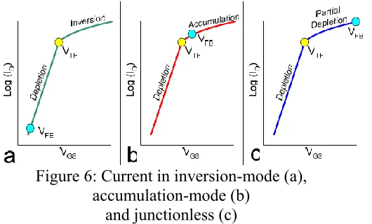
Depletion of the heavily doped nanowire creates a large electric field perpendicular to current flow below threshold, but above threshold the field drops to zero. This is the opposite of inversion-mode (IM) or even accumulation mode (AM) devices where the field is highest when the device is turned on. The electron concentration profiles in cross sections of IM, AM and JNT devices are shown in Figures 6
Figure 6: Current in inversion-mode (a), accumulation-mode (b)
and junctionless (c)
[1] Dan Rosso.―Semiconductor Industry Posts Record Sales In 2013. ‖Internet :https://www.semiconductors.org/ news/ 2014/03 /global sales reports 2013 semiconductor industry posts record sales in 2013 3rd February 2014, [10 th February,2014]
[2] Moore, Gordon E. (1965). "Cramming more components onto integrated circuits" (PDF). Electronics Magazine. p. 4. Retrieved 2006-11-11.
[3] Taur, Yuan ―Invited talk: CMOS device scaling — Past, present, and future‖ Microelectronics And Electron Devices (WMED), 2014 IEEE Workshop On, 18-18 April 2014.
[4] A. Toriumi, M. Iwase, and M. Yoshimi, ―On the performance limit for Si MOSFET: Experimental study,‖ IEEE Trans. Electron Devices, vol. 35, pp. 999–1003, 1988
[5] Farzin Assad, Zhibin Ren, Dragica Vasileska, Member, Supriyo Datta, Mark Lundstrom, ―On the Performance Limits for Si MOSFET’s Theoretical Study‖, IEEE Transactions On Electron Devices, Vol. 47, No. 1, January 2000.
[6] ITRS Update 2012, Available Online:
www.itrs.net/Links/2012ITRS/Home2012.htm[10th
February,2014]
[7] Morten, B. ; Canali, C. ; Ferla, G. ; Taroni, A.―Strain Sensitivity of MOSFET Devices‖ Instrumentation and Measurement, IEEE Transactions on (Volume: 26 , Issue: 4 ),Dec. 1977.
[8] Lam, H.W, Sobczak, Z.B, Pinizzotto, R.F, Tasch, A.F, ―MOSFETs Fabricated in {100} single crystal silicon-on-oxide obtained by a laser-induced lateral seeding technique‖ Electron Devices Meeting, 1980 International (Volume: 26 ),1980.
[9] Xuejue Huang, Wen-Chin Lee, Charles Kuo, Hisamoto, D, Leland Chang, Kedzierski, J, Anderson, E, Takeuchi, H. ; Yang- Kyu Choi ; Asano, K, Subramanian, V, Tsu-Jae King, Bokor, J, Chenming Hu, ―Sub 50-nm FinFET: PMOS‖, Electron Devices Meeting, 1999. IEDM '99. Technical Digest. International,pp.67 – 70,5-8 Dec. 1999.
[10] Hisamoto, D, Wen-Chin Lee, Kedzierski, J, Takeuchi, H, Asano, K, Kuo, C, Anderson, Erik, Tsu-Jae King, Bokor, J, Chenming Hu, ―FinFET-a self-aligned double-gate MOSFET scalable to 20 nm‖ Electron Devices, IEEE Transactions on (Volume:47 , Issue: 12 ), pp.2320 – 232, Dec 2000.
[11] Chenming Hu , ―SOI and nanoscale MOSFETs‖ Device Research Conference,pp.3 – 4, 2001,25-27 June 2001
.
Chenming Hu―Sub-50 nm P-channel FinFET‖, Electron Devices, IEEE Transactions on (Volume:48 , Issue: 5 ), pp. 880 – 886, May 2001.
[13] Tang, S.H, Chang, L, Lindert, N, Yang-Kyu Choi, Wen-Chin Lee, Xuejue Huang, Subramanian, V., Bokor, J, Tsu-Jae King, Chenming Hu, ―FinFET-a quasi-planar double-gate MOSFET‖ , Solid-State Circuits Conference, 2001. Digest of Technical Papers. ISSCC. 2001 IEEE International, pp. 118 – 11
[14] J.P.Colinge,et.al,―Nanowire transistors without junctions‖ Nature nanotechnology,Vol.5,[Online] https://www.nature.com/naturenanotechnology, March, 2010.
[15] Chi-Woo Lee, Adrien Borne, Isabelle Ferain, Aryan Afzalian, Member, IEEE, Ran Yan, Nima Dehdashti Akhavan, Pedram Razavi, and Jean-Pierre Colinge, Fellow, IEEE, ―High-Temperature Performance of Silicon Junctionless MOSFETs‖
IEEE TRANSACTIONS ON ELECTRON
![Figure 3: Current Voltage Characteristics [14] Junctionless simplified, compared to standard CMOS since there are no doping concentration gradients in the device](https://thumb-us.123doks.com/thumbv2/123dok_us/7751318.1270786/3.612.38.262.367.519/current-voltage-characteristics-junctionless-simplified-compared-concentration-gradients.webp)