Available online: https://edupediapublications.org/journals/index.php/IJR/ P a g e | 1 8 6 5
Low Power BIST based Multiplier Design and
Simulation using FPGA
MR. D. SRIDHAR, ASSOCIA TE PROFESSOR, DEPA RTM ENT OF ECE
G.KALYANI,B.VEERANE, CH.L. PAVAN KUMAR GUPT A, E. PHANI PAVAN PRAKASH,CH.AKHIL BABU
B.Tech Students , Department of Electronics & Communication Engineering, Ramachandra College of Engineering, Eluru, Andhra Pradesh, India.
Abstract – The ever increasing applications of integratedcircuits in t he day-to-day useful electronic gadgets is the driving force for the development of low power designs of configurable hardware designs. High speed and low power are the main parameters that are target ed by modern circuit designers. Among t he fast est increasing applications the audio and video signal processing applicat ions are growing at a very high rate. Mobile applications have increased t he t echnological imp rovement s for digit al signal p rocessing applications. Multipliers are the very important logic operational unit of any processing unit in digital signal processing applications. T he sp eed and performance of mult ip lier is among t he efficiency imp rovement parameters of any digital hardw are design. Anot her imp ortant feature of hardware designs is self -test ing abilit y . T his feature provides reliabilit y t o t he hardware mainly in case of configurable hardware applications. The built-in-self-t est (BIST ) feature help s in quick diagnosis of t he hardware funct ional aut henticity. This paper presents a BIST based implementat ion of a multiplier. The proposed design is realized using Xilinx T ool using VHDL. A low power Test Pattern Generator (TPG) is involved in the design for self-t est design realiz at ion.
Keywords– Built-In-Self-Test, Test Pattern Generat or, Linear Feedback Shift Regist er, Xilinx, VHDL.
I.INTRODUCTION
Nowadays, a configurable hardware design performance can be evaluated using its operational speed and power. Field Programmable Gate Array (FPGA) is among the configurable devices that cope with the desired and promising power and speed based hardware performance. In FPGA the operation execution is based on the switching of the internal path of current through a combination of hardware resource architecture. A hardware based optimization of any design can be achieved by the skill based modification of the operational circuit architecture. A low power system offers the benefits like device portability, long battery life, good performance criteria, etc.
For modern digital applications a high speed processor with low power requirement design is the basic criteria. The most important design of digital signal processors is the multiplier design. The multiplier is used in most of the complex data processing applications. The self-testing feature is another feature that is required in the hardware for self-
diagnosis or self- testing.
This feature helps the configurable integrated circuit hardware to test itself and in case of hardware fault it helps to re-locate the hardware resource within the integrated circuit. In the self-test operation, hardware is self-tested for its functional output with the help of a supplementary hardware. A simple block diagram of a BIST based design representation is shown in Fig 1. Here a Logic Circuit is the design that is a functional block of an integrated circuit hardware design. In the normal operation mode it performs the defined logic operation on DATA Input. When it is operated in Self -Test mode, a random sequence of data is generated by Test pattern Generator using control signal by BIST Controller. This test sequence is operated by Logic Circuit and the generated output of the logic operation is compared with the actual output. The comparator output indicates logic high if the output of the logic operation against the test inputs does not match with the actual output. This condition indicates a fault in the logic circuit hardware. In such cases a configurable hardware re-locates the circuit resources within the integrated circuit to avoid the faulty hardware.
Available online: https://edupediapublications.org/journals/index.php/IJR/ P a g e | 1 8 6 6
Many architectural modifications are proposed by many scholars and researchers in their work regarding low power design of BIST based logic circuit for hardware design applications. In [1] a low power test pattern generator design is proposed using a low-power Linear Feedback Shift Register for BIST structures. This design follows the approach of reducing the switching activity based on single input change pattern generated by a counter and a gray-code converter. Reference [2] presents FPGA Implementation of an LFSR based Pseudorandom Pattern Generator for MEMS Testing. This design has the characteristics of high speed, low power consumption and it is especially suited in the processors where uniform distribution random numbers are required. A Low Power linear feedback shift register based low power test pattern generator design is proposed in [3]. This design mainly focuses on how test vectors are generated in the BIST and how to reduce the power consumption. In this paper the transition is reduced by generating the gray-code with 1-bit distance. Reference [4] shows FPGA implementation of 16-bit BBS and LFSR PN Sequence Generator. This paper features the change in the logic of PN sequence generator by changing the seed in LFSR or by changing the key used in BBS.
A paper with FPGA based N-bit LFSR to generate random sequence number design is proposed in [5]. This design presents study the performance and analysis of the behavior of randomness in LFSR. A review of LP-TPG using LP-LFSR for Switching Activities is presented in [6]. This paper presents structures of multiplier, LFSR, LP-TPG and BIST. In [7] the author presents a simulation study of TPG using Shift Register based on 16th Degree Primitive Polynomials. The study in this paper focuses on a comparative study of different types of implementations for a LFSR for 16 th degree irreducible or primitive polynomials. Generation of Pseudo -Random number by using WELL and Re-seeding method is presented in [8]. In this paper a random number is generated by using WELL method first and its performance was analyzed. For avoiding the repeating pattern the Re-seeding method is used. A number of researches are also performed on logic operational units for high speed applications using FPGA devices.
A review on Vedic Mathematics for digital signal processing operations is present in [9]. This paper deals with exhaustive review of literature based on Vedic Mathematics. An improved efficiency of Vedic multiplier is proved over conventional multiplier in this paper. An FPGA based implementation of high speed 16-bit Vedic multiplier using LFSR is presented in [10]. This paper describes the implementation of 16- bit Vedic multiplier enhanced with propagation delay and automatic insertion of all possible combinations of inputs. The TPG is the major component of BIST hardware design. Many BIST application circuits are proposed and simulated by researchers to propose power and speed optimized designs based on FPGA implementation. Reference [11] presents FPGA implementation of BIST
enabled UART for Real Time Interface Applications. This paper shows functional verification of various block of UART. A concurrent BIST architecture for online input vector monitoring design is proposed in [12]. This paper is based on the idea of monitoring a set of vectors reaching the circuit inputs at the time of normal operation and the use of a SRAM like architecture that store the relative locations of the vectors that reach the circuit inputs. A BIST enabled I2C protocol design implementation on FPGA is presented in [13]. This design enables self-test of a common hardware interface protocol for high speed communication device.
The requirement of the today’s hardware designs is low power circuit implementation of BIST based logic circuits on FPGA to achieve high speed operational circuits. Reference [14] shows an advanced BIST architecture with Low Power LBIST and BDS oriented March Algorithm for Intra Word Coupling Faults. This paper addresses read faults with classic faults with an improvement in the efficiency of the architecture and test time in detecting the faults. In the present paper a critical consideration is given to low power BIST implementation. A multiplier with two 4-bit inputs is taken as a test design for low power implementation on FPGA with self-test capability. The self-test feature is provided using a low-power test pattern generator design. The test pattern is designed using a modified architecture by reducing the number of sequential component as compared to the conventional design components. The present paper is organized as follows: Section-II describes the design of Test Pattern Generator and Multiplier that are implemented in this work. Section-III presents simulation and synthesis results. Section-IV presents the conclusion drawn on the basis of the performed design. Finally the references are mentioned.
II.TEST PATTERN GENERATOR AND MULTIPLIER DESIGN
The present work gives the BIST based approach for the implementation of a multiplier using a configurable hardware. A 4-bit low power multiplier design is used as a test logic design in the present work. The multiplier design is implemented using gate level architecture representation for realizing the low -power hardware. The RTL schematic of the multiplier design on Xilinx Synthesis Tool is shown in Fig 2. A gate level combination is used to generate a half-adder and a full-adder design. These adder design block are used in combination to generate the multiplier using the adder terms.
Available online: https://edupediapublications.org/journals/index.php/IJR/ P a g e | 1 8 6 7
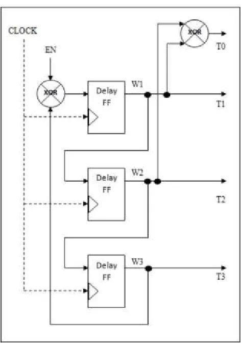
logic block diagram of the test pattern generator is shown in Fig 4. Three flip -flop with linear feed-back are used. The output of the last flip-flop is XOR-ed with the control input Enable to initiate the random number generation. The outputs of the first two flip-flops are XOR-ed to generate the fourth output bit of the TPG. Thus if Enable input is low then the output of the TPG will drive to logic “0000” output combination. An active high signal on the Enable input will activate the hardware to generate random 4-bit signal. The presented TPG can be used in multiple combinations, serial or parallel or mixed, for generating a random sequence of number with a higher length for many other BIST based application realization. This circuit generates a 4-bit random value using only 3-registers, so relative low power consumption is caused by this circuit. RTL schematic the test pattern generator is shown in Fig 5.
Fig. 4 Flow Diagram of Random Sequence Generation by TPG
Fig. 2 RT L Schematic of Proposed T est Multiplier
Available online: https://edupediapublications.org/journals/index.php/IJR/ P a g e | 1 8 6 8
Fig. 5 RT L Schematic of 4-bit Test Pattern Generator
III.SIMULATION AND SYNTHESIS RESULTS
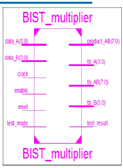
The BIST based Multiplier design in the proposed work is implemented using VHDL Hardware Description Language on Xilinx ISE Tool. The RTL block diagram of the proposed design is shown in Fig. 6. The simulation of the complete design is performed on Xilinx ISim Tool using VHDL Test-Bench. The waveform simulation result of the BIST-multiplier and the multiplier designs are shown in Fig 7 and Fig 8 respectively. The design is simulated for functional performance and power consumption.
Fig. 6 RT L Block Diagram of Proposed Design
The power consumption analysis is performed on multiple frequencies and different integrated circuits (FPGAs) with different internal and auxiliary voltage specifications. Xilinx FPGA devices from Kintex-7, Vertex-6 and Spartan-6 family devices are used for analyzing dynamic power consumption of the present BIST multiplier design. The dynamic power consumption of the FPGAs is presented in Table 1. The power-frequency analysis of the proposed work is performed using Xilinx XPower Tool.
Fig. 7 Waveform Simulation of Proposed Multiplier
T ABLE I
FREQUENCY VS DYNAMIC POWER CONSUMPT ION OF PROPOSED DESIGN ON FPGA OPERATING AT DIFFERENT VOLTAGE
Voltage Freq. Dynamic Total
Device Power Power
VCCint VCCaux MHz (W) (W)
XC6S LX 150 -
1.2 V 2.5 V 1000 0.198 0.318
Available online: https://edupediapublications.org/journals/index.php/IJR/ P a g e | 1 8 6 9
500 0.099 0.216 1000 0.216 1.514
XC6VC X 75T -
1.0 V 2.5 V 800 0.173 1.470
2FF484
500 0.108 1.403
XC7K70T - 1000 0.114 0.222
1.0 V 1.8 V 800 0.091 0.199
2LFB G6 76
500 0.057 0.165
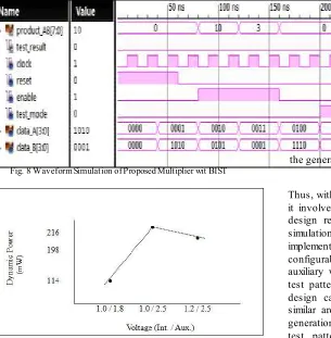
Fig 9 shows the Dynamic power variation of the proposed design at a constant frequency of 1GHz against the chip voltages for Kintex-7, Vertex-6 and Spartan-6 FPGA devices. The device specification number is mentioned in Table I. The conclusion from this observation clearly specifies that Kintex-7 device shows the least power consumption for the present circuit among the three devices. Fig 10 represents the graph of Dynamic Power variation of the proposed design with respect to the variation in the operational clock frequency on Kintex-7 device. The graph shows a linear variation in the dynamic power with respect to the clock frequency.
Fig. 10 Frequency Versus Dynamic Power variation of proposed design for Kintex-7 Family FPGA Device
IV. CONCLUSION
In the present work the logic design that is used in the built-in-self-test application is a 4 -bit multiplier and the test pattern generator is also designed for generating a random 4-bit number. The test pattern generator is a modified design that has a low register-to-bit ratio, i.e., the number of out bits in the generated sequence is more than the number of registers in
the generator circuit. Fig. 8 Waveform Simulation of Proposed Multiplier wit BIST
Fig. 9 Chip Voltage Versus Dynamic Power variation of proposed design at 1GHz Frequency for Kintex-7, Vertex-6 and Spartan-6 Family FPGA Devices
Available online: https://edupediapublications.org/journals/index.php/IJR/ P a g e | 1 8 7 0
as the scope of combining other existing hardware designs with this design for a complex logic implementation.
REFERENCES
[1] A. Kavitha, G. Seetharaman, T. N. Prabhakar and Shrinithi, “Design of Low Power T PG using LP -LFSR”, International Conference on Intelligent Systems Modelling and Simulation, IEEE Computer Society, pp.334-338, 2012.
[2] Md. Fokhrul Islam, M. A. Mohd. Ali and Burhanuddin Yeop Majlis, “FPGA Implementation of an LFSR based Pseudorandom Pattern Generator for MEMS T esting”, International Journal of Computer Applications, Volume-75 No-11, pp.30-34, August 2013.
[3] Syed. Mujeeb Raheman and M. Basha, “ Low Power Linear Feedback Shift Register based Low Power T est Pattern Generator”, International Journal and Magazine of Engineering, T echnology, Management and Research, Volume-2 Issue-6, pp.579-584, June 2015.
[4] Mohammad Moinuddin and Sadgunn Kumari V, “FP GA implementation of 16-bit BBS and LFSR PN Sequence Generator”, International Journal of Scientific Engineering and T echnology Research, Volume-4 Issue-31, pp.6082-6084, August 2015. [5] Babitha P. K., T hushara T . and Dechakka M.P., “FPGA based N-bit
LFSR to generate random sequence number”, International Journal of Engineering Research and General Science, Volume-3 Issue-3, pp.6-10, May-June 2015.
[6] Swapna S. and Sunilkumar S. Manvi, “Review of LP -T PG using LP-LFSR for Switching Activities”, International Journal of Advanced Research in Computer Science and Software Engineering, Volume-5 Issue-2, pp.157-160, February 2015.
[7] Mirella Amelia Mioc, “A simulation study of T PG using Shift Register based on 16th Degree Primitive Polynomials”, New Developments in
Pure and Applied Mathematics, pp.363-369, ISBN: 978-1-61804-287-3. [8] V. Divya Bharathi and Arivasanth M., “Generation of Pseudo-Random number by using Well and Re-seeding method”, International Journal of Advanced Research in Electronics and Communication Engineering, Volume-4 Issue-3, pp.604-609, March 2015.
[9] Kaustubh M. Gaikwad and Mahesh S. Chavan, “Vedic Mathematics for Digital Signal Processing Operations: A Review”, International Journal of Computer Applications, Volume-113 N0-18, pp.10-14, March 2015. [10] Neha Shaktawat and Ghanshyam Jangid, “FPGA Implementation of High Speed 16-Bits Vedic Multiplier using LFSR”, International Journal of Computer Science and Mobile Computing, Volume-4 Issue-8, pp.102-108, August 2015.
[11] L. Supriya, J. Lingaiah and G. Kalyan, “FPGA Implementation of BIST (Built-in-Self-T est) Enabled UART for Real T ime Interface Applications”, International Journal of Science, Engineering and T echnology Research, Volume-4 Issue-7, pp.2645-2647, July 2015. [12] S. Abirami, Nikitha S. Paulin, S. Prabhu Venkateshwaran, “A concurrent BIST architecture for online input vector monitoring”, International conference on Science, Technology and Management, pp.1411-1488, Feb 2015.