ABSTRACT
LEWIS, MATTHEW SCOTT. The Utilization of Scanning Probe Lithography to Interrogate Both Self Assembled Monolayers and the Nanostructures Created Therein via Scanning Tunneling Microscopy. (Under the direction of Dr. Christopher B. Gorman.)
The Utilization of Scanning Probe Lithography to Interrogate Both Self Assembled Monolayers and the Nanostructures Created Therein
via Scanning Tunneling Microscopy
by
Matthew Scott Lewis
A thesis submitted to the Graduate Faculty of North Carolina State University
in partial fulfillment of the requirements for the Degree of
Master of Science
Chemistry
Raleigh, North Carolina 2013
APPROVED BY:
_______________________________ ______________________________
Dr. Tatyana Smirnova Dr. Edmond Bowden
________________________________ Dr. Christopher B. Gorman
DEDICATION
To Jodee Marie the love of my life. Your love and support is what keeps me going when the pain seems insurmountable. I will always strive to make you proud.
BIOGRAPHY
ACKNOWLEDGMENTS
I would like the thank Dr. Christopher Gorman for his assistance in helping me to better understand both the experiments that I ran and how to think like a graduate level researcher. I would like to thank Dr. David Shultz for helping me realize a dream. I would like to thank Ryan Fuirer and Dr. Stephan Krämer for the discussions that we had on my science and the field of molecular electronics and for first showing the capabilities and proper procedure of the STM which placed the keys to molecular resolution at my fingertips. I would also like to thank James Williams who is always a great sounding board and with whom I have had many great discussions and a great friendship. I would also like to thank Young Ray Hong and Namjim Kim both of whom have been very helpful with my science and with other aspects of graduate school. Finally I would like to thank my best friend and loving wife, Jodee. Jodee has proofread my documents, been a sounding board for both science on non-science discussions and has most importantly always been there when I needed her support especially over the last few years when my disease and its cures were at their worst. Thank You Jodee I would have never gotten this far without you.
TABLE OF CONTENTS
LIST OF FIGURES ... ... v
Chapter 1 Patterned Self Assembled Monolayers via Scanning Probe Lithography ... ...1
1.1 Introduction ...2
1.2 Elimination Lithography ...3
1.3 Addition Lithography ...7
1.4 Substitution Lithography ... ...11
1.5 Apparent Height ...14
1.6 Concluding Thoughts ... ...16
1.7 References ... ...18
Chapter 2 Scanning Tunneling Microscope-Based Replacement Lithography on Self-Assembled Monolayers. Investigation of the Relationship Between Monolayer Structure and Replacement Bias ...22
2.1 Impetus ...23
2.2 Results and Discussion ...23
2.3 Conclusions ... ...31
2.4 Experimental ... ...31
2.5 References ...33
Chapter 3 The Utilization of Replacement Lithography to Create Nanostructures of Various Ferrocenyl Terminus Alkanethiols with and without β Ketone on Au (111) and Studied via Scanning Tunneling Microscopy ...34
3.1 Introduction ... ...35
3.2 Methods ...38
3.3 Premise ... ....40
3.4 Results and Discussion ... ...42
3.5 Conclusions ... ...46
3.6 Experimental ...48
LIST OF FIGURES
Chapter I
Patterned Self-Assembled Monolayers via Scanning Probe Lithography
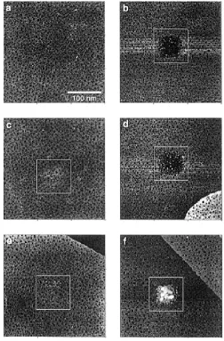
Figure 1.1. 300 nm x 300 nm scanned image via STM of an n-octadecyl mercaptan SAM with a centralized 50 nm x 50 nm patterned region fabricated under varying relative humidity from ~75% for images (a), (b), (d), and (f) and ~6% for (c) and (e). Also the imaged surface in (a) represents a prepatterned surface; were as, (b)-(e) contain the patterned feature at a bias of 3.0 V and (f) at -3.0 V. Reprinted with permission from [5], Copyright 1996, American Chemical Society ...5
Figure 1.2. Height mode AFM images of (a) 1-octadecyne, (c) 1-dodecyne, and (e) 1,4-diethynylbenzene electrografted patterns on hydride terminated Si and the corresponding frictional images (b), (d), and (f) respectively. Reprinted with permission from 26, Copyright 2003, American Chemical Society ... ...8
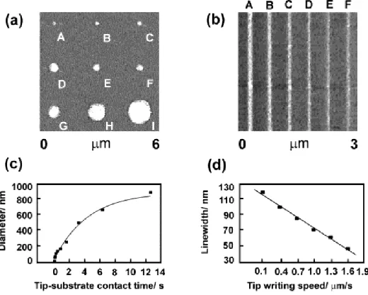
Figure 1.3 (a) An array of features scaling from 45 nm to 920 nm in diameter generated by varying the contact time during the MHA writing phase with contact time increasing from A-I backfilled with ODT and developed with magnetic nanoparticles. (b) Lines produced by varying writing speeds from 0.1 µm/s to 1.3 µm/s creating line widths of 120 nm to 60 nm scaled from A-F. (c) A study of contact time versus feature diameter plotted via analysis of
(a). (d) A plot of writing speed compared to fabricated line widths produced in (b). Reprinted with permission from32, Copyright 2002, WILEY-VCH Verlag GmbH ....9
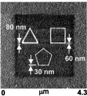
Figure 1.4. Polygons written with MHA preformed with varying writing times. The darkened square 3 µm x 3 µm region was patterned afterwards by writing with ODT. Reprinted with permission from30, Copyright 1999, American Association for the Advancement of Science ...10
Figure 1.5.(A) An AFM image of C10S SAM prior to fabrication. (B) Patterning of two 10
nm x 50 nm C18S- lines with 20 nm spacing. (C) Removal of one of the C18S- lines and
reintroduction of the C10S- into the region. (D) Fabricating another C18S- line 65nm in length.
Reprinted with permission from48, Copyright 1999, American Chemical Society ..13
Figure 1.6. Replacement lithography images showing an FcC11SH molecules replaced into a
C12S-SAM. Also illustrated is bias dependent apparent height contrast shown by the dark
Figure 1.7. A series of replacement lithography experiments imaged by STM with FcC11S-
as replacing molecule and background monolayer indicated at the left side of each image. Each scanned image illustrates the effect of varying the applied bias within each monolayer while maintaining constant humidity ~55% and writing speed 20 nm/s. Reprinted with permission from54, Copyright 2004, American Chemical Society ...17
Chapter II
Scanning Tunneling Microscope-based Replacement Lithography on Self-Assembled Monolayers. Investigation of the Relationship Between Monolayer Structure and Replacement Bias
Figure 2.1. Sample preparation. (A) represents a gold wire attached to a platinum disk via gold “glue”. (B) illustrates aligning a facet on the gold bead parallel to the platinum disk. (C) represents the platinum disk in an ethanolic solution. (D) is an illustration of the typical vial type used for refluxing the sample ...24
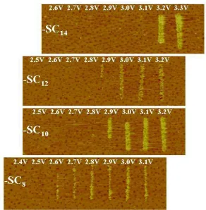
Figure 2.2. A series of STM images in which replacement lithography was attempted at incrementally higher biases. The designation -SCn denotes the chain length of the initial SAM. A series of lines of 100 nm length were written with the biases indicated above each line. Imaging Conditions: z-scale = 3 nm; relative humidity = 55% ± 2 %; imaging bias = 1.5 V; setpoint current = 10 pA, scan rate = 1.0 Hz; under dodecane ...25
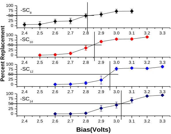
Figure 2.3. Graph indicating the percentage of replacement for different CnS-SAMs (n is the number of carbons in the alkylthiol of the initial self assembled monolayer). T bars are drawn to aid in ascertaining the replacement bias required to affect 50% replacement. Error bars are at the 90% confidence interval. Lines are drawn through the points solely as a guide to the eye ...26
Figure 2.4. Illustration of the possible effects found in less ordered self assembled monolayers. In this schematic the adsorbed molecules (blue terminus) are blocking the replacement molecules (black terminus from approaching the surface ...28
Figure 2.5. A series of STM images in which replacement lithography was attempted at incrementally higher biases on the self assembled monolayers indicated to the left of each image. The numbers above each line represent the applied bias used to effect replacement in that line region. Imaging Conditions: z-scale = 3 nm; relative humidity = 55% ± 2 %; imaging bias = 1.25 V for -SC10CN and -SC10CO2H and 1.5 V for -SC11OH; setpoint current
Chapter III
The Utilization of Replacement Lithography to Create Nanostructures of Various Ferrocenyl Terminus Alkanethiols with and without β Ketone on Au (111) and Studied via Scanning Tunneling Microscopy.
Figure 3.1. An illustration of Negative Differential Resistance with the blue box region highlighting the region where the current decreases as the bias continues to increase
...36
Figure 3.2. An illustration of the replacement lithography process. In this description an elevated positive bias is affected between the tip and substrate under an inert solvent (dodecane) to which a secondary thiol has been added. The elevated bias causes the background self-assembled monolayer SAM (dodecanethiolate in this case) to desorb and to be “replaced” with the molecule of interest ...39
Figure 3.3. Structure of the replacement inks used. Herein Ferrocenyl undecanethiol will be referred to as FcC11 Ferrocenyl hexanethiol as FcC6 Ferrocenyl-11-undecanonethiol as
FcCOC10 and Ferrocenyl-6-hexanonethiol as FcCOC5 ...40
Figure 3.4 The gold lines represent the Fermi levels for the substrate 6.3 eV and the gray lines for the tip 5.6 eV in the theoretical metal molecule metal junction while the red lines represent the HOMO of the FcCO(CH2)n species 5.75 eV and the blue lines represent the
Fc(CH2)n species 5.5 eV and the dashed line represents the Fermi level of the Normal
Hydrogen Electrode (NHE). The diagram on the left shows the metal-molecule-metal junction at a bias of 0V where the diagram on the right illustrates the same junction bias of +1V. In this particular junction the tip, which is negatively charged, shifts its Fermi level down and the sample, which is positive, shifts its Fermi level up ...42
Figure 3.5. An illustration of the process of rinsing the STM cells necessary for creating two ink nanostructures. (A) The removal of the old dodecane solution containing the first ink. (B) The addition of a fresh dodecane solution using a different solution from step A. (C) represents the repetition (5 cycles) of steps A and B ...43
Figure 3.7 An illustration of the apparent height (which is the difference between the registered height of the molecule of interest compared to the background) Vs bias of FcC11S-Au , FcC6S-Au , FcCOC10S-Au, and FcCOC5S-Au. The red lines represent the 95% confidence interval for each point. The error was determined from either a Gaussian or Lorentzian fit of greater than 5000 pixels per point ...45
Figure 3.8 The gold lines represent the Fermi levels for the substrate 6.3 eV and the gray lines for the tip 5.6 eV in the theoretical metal molecule metal junction while the red lines represent the HOMO of the FcCO(CH2)n species 5.75 eV and the blue lines represent the
Fc(CH2)n species 5.5 eV and the dashed line represents the Fermi level of the Normal
Chapter 1
Patterned Self-Assembled Monolayers via
Scanning Probe Lithography
1.1 Introduction
Scanning probes have been used to induce a variety of localized changes in the composition of self-assembled monolayers (SAMs). SAMs are useful in this regard because they offer a means to present various chemical functionalities at a surface in a relatively well organized way. This chapter reviews a diverse set of methodologies. However, they all can be generally characterized as either additive (adding molecules to the surface), subtractive (removing molecules from the surface) or exchange (a replacement of one type of molecule for another on the surface. The efficacy and utility of these processes will be emphasized.
Looking back into human history, one finds diverse forms of lithography to communicate ideas and creeds. The substrates include cave walls, tablets, and canvas used for paintings, carvings, and diverse forms of writing and art. Each of these substrates requires a different form of lithography: the process of elimination for carving or the process of addition for painting and writing.
In tracing the development of each form of lithography, the simplest and most useful means of fabrication dominated the earliest efforts. Initially the use of a series of markings on individual tools allowed the identification and possession of personal effects. The concept of elimination lithography rests on the precept that features removed from the surface are fabricated through a series of scratches. This system only requires a flat surface and a sharp rock, much like some current nanolithography schemes.
These techniques can be translated into the modern day areas of nanolithography through the use of scanning probe lithography. With scanning probe lithography it is possible to remove material from the substrate via elimination or add to the surface via addition or do both via substitution. Each of these methods have their own unique advantages and disadvantages which will be discussed in the proceeding chapter.
more complete coverage of this subject1. The main topic that will be discussed in this chapter is that of alkyl thiolate monolayers on single crystalline gold substrate. Through the examples provided here, it will emerge that this system is one of the most robust and flexible on this length scale. These properties account for its ubiquitous use in nanometer-scale lithography.
1.2 Elimination Lithography
Elimination lithography can be thought of as the oldest form of writing beginning with the ancient cultures carving symbols into stone more than 4000 years ago. Today our techniques are more sophisticated but they are based on the same principle of removing material to create patterns1, 2. Line resolution using elimination lithography varies with the substrate and monolayer with the highest resolution being near 10 nanometers. The first example of probe-based elimination lithography employed a scanning tunneling microscope (STM). Crooks et al 3-6 created geometrically well defined structures with a range of dimensions from 60 nanometers (nm) to 5 micrometers (µm). This was accomplished by first preparing a gold bead in a dihydrogen flame in order to form a faceted Au (111) surface. The faceted surface was then exposed to a 1 millimolar ethanolic solution of octadecanethiol for 24 hours. The smaller features of circa 60 nm were fabricated by elevating the tip bias to 3 V while the larger 5 µm2 regions were obtained by using a more substantial 8 V tip-sample bias. The measured thickness of the patterns, 0.7 nm, was not equal to the ellipsometric thickness of the octadecanethiolate monolayer (ca 2.2 - 2.8 nm) 3.
To address this apparent disparity in thickness, the authors used Ru(NH3)6+3 to
line measured depth and ellipsometrically measured thickness of the self-assembled monolayer (SAM) was a reflection of the different conductances through the SAM-covered and bare regions 3. Thus, as probed by STM, the SAM appeared taller relative to the underlying gold than would be expected just from the topographic differences. The mechanism of this transformation is postulated to be electrochemical in nature 3-6. This conjecture has been supported by the results of experiments in which the ability to desorb a monolayer with increased tip-substrate bias was directly related to the relative humidity (Fig. 1.1). To establish this relationship, Crooks et al 3-6 investigated the influence of relative humidity on the desorption of n-octadecane thiolate monolayers from Au. To characterize this process, 50 x 50 nm2 squares were removed from the SAM while the relative humidity was controlled. A higher relative humidity facilitated the process. Interestingly, the application of a reverse bias failed to desorb the monolayer; instead it appeared that material from the tip deposited onto the surface.
One impetus for studying the desorption of SAMs was based on the idea that they could serve as well-controlled, ultrathin resists. To this end, Craighead et al. 7 investigated the use of an etched tungsten STM tip as a source for low energy electrons to modify a surface of an octadecanethiolate SAM grown on both gold and gallium arsenide (GaAs). Using the SAM/gold system they were able to create lines with a resolution limit of 25 nm. Using the SAM/GaAs system, 20 nm lines were produced as determined by AFM. Lithography on both the gold and the GaAs systems resulted in raised features unless the current and voltage values were sufficiently high or low to cause the tip to contact the surface and mechanically remove the monolayer 7.
can mechanically disrupt the SAM at elevated setpoint force. It may be the case, however that the tip mechanically disrupts the SAM in STM as well2, 9. The first example of elimination lithography on a SAM with AFM was shown on alkanethiolate monolayers on
gold 8. In this example, while scanning over a region, the applied tip force was increased and local degradation of the monolayer was noted 8. Subsequently, other examples have been illustrated showing the removal of both double-stranded DNA 10 and single-stranded DNA 11 from gold.
Another example of elimination lithography on SAMs has been performed using current sensing atomic force microscopy (CS-AFM) 12 also known as conducting probe AFM (CP-AFM) 13. The CS-AFM has the capabilities of normal AFM combined with current sensing abilities similar to that of STM 2. The instrument allows the simultaneous measurement of the surface topography and I-V curves and has the advantage being able to determine the lateral location of the tip with respect to various domain and other topographic features associated within the monolayer with a high degree of precision13-16. Using CS-AFM, Uosaki, et al. 12 were able to remove an octadecanethiolate monolayer from beneath the tip by applying a bias between the tip and substrate. This removal was detected by an increased current in lithographically patterned regions of SAM as well as topographical depressions with a depth corresponding to that of the thickness of the SAM 12. Further experiments into the elimination mechanism of this technique illustrated that the bias required to remove the SAM was dependent on relative humidity 17 as had been observed previously by Crooks et al 6.
single gold colloids were trapped 20, elucidation as to how surface charge was accumulated as a function of applied bias 21, and patterning of alkyl monolayers 22.
1.3 Addition Lithography
The second oldest form of writing and perhaps the oldest form of artwork is that of addition lithography. Addition lithography is based on a concept that is very familiar to society, writing with an ink on blank paper. There are several different methods for patterning monolayers using micropens, nanopipets, and microcontact printing (μCP) 1, 23-25
. In this vein, one finds the use of an inked AFM for this type of writing. Since the feedback signal in STM is current, and any material on the tip will have a large influence on tunneling probability, the idea of an inked tip is not amenable to STM.
Dip-pen nanolithography (DPN) employs an AFM tip coated with some material as a writing implement on a surface 27. In DPN an AFM tip is “inked” with a solution that will self-assemble or otherwise adhere onto the surface of choice. The tip is then brought into contact with the surface at which point a water meniscus is formed which is believed to facilitate in the transportation of the ink from the tip to the substrate. Since the first demonstration of DPN 28-31 this procedure has been used in both tapping and contact mode to pattern various substrates from gold and mica to silicon and gallium arsenide with inks ranging from alkyl thiols to proteins 27.
In one interesting example, Liu and coworkers explored the use of magnetic nanoparticles, manganese ferrite (MnFe2O4), attached to patterned 16-mercaptohexadecanoic
acid, MHA 32. The fabrication of magnetic nanostructures has implications in various fields such as the development of magnetic storage devices which increase in capacity as the density of magnetic features increase. Liu et al. created magnetic structures via DPN by patterning MHA on a gold substrate then immersing in a 1-octadecanethiol, ODT solution to
back-fill the remaining bare gold regions. The sample was then dipped in nanoparticle solution. To characterize the fabrication process, various stationary exposure times of the cantilever to the substrate as well as writing speeds were recorded for the initial formation of MHA monolayers followed by previously established procedures.
Notably, Liu et al. observed that the variation of contact time and writing speed generated two different behaviors. The feature size as a function of contact time produced a nonlinear response that differed when compared to the variation of writing speed (Fig. 1.3). However, most notable was the facilitation of nanoparticle attachment to MHA-covered regions of the surface but not to ODT-covered regions.
Hong and coworkers examined the feasibility of patterning multiple “inks” with DPN31. In their investigation, the application of multiple inks required the use of a closed loop AFM. Closed loop AFM allowed the use of alignment markers to ensure more accurate alignment and positioning of the AFM tip. The features observed (Fig 1.4) were produced as a result of patterning MHA at a writing speed, the variation of which facilitated the control of the line width. Then the AFM tip coated with MHA was exchanged with an ODT coated one, and rastering the tip over a 3 µm size square resulted in a backfilling with the ODT to create the darkened region surrounding the geometric features. The precision of line placement, control of thermal drift (>1 nm/min), and application of multiple inks onto a single substrate provides avenues into exploring and comparing multiple SAMs simultaneously.
Another interesting use for DPN is for the creation of templates. This method involves patterning the surface with a substituent that will bind the “material of interest”. This method has been used to create patterns of various proteins and nanoparticles 33, 34 and the scope of this work has been reviewed extensively 1 , 27.
There are several questions that still exist on the fundamental mechanism that drives DPN. The mechanism of ink transport by the water meniscus is one of these questions. Another is the method by which hydrophobic molecules are transferred through this water meniscus, and yet another focuses on the need for the water meniscus. To date, the answers to these questions are still up for speculation with some arguing both for 35 and against 36, 37 the necessity of the water meniscus. These experiments and their interpretation are reviewed in more detail elsewhere1, 27.
1.4 Substitution Lithography
The third form of writing is that of substitution lithography where first the background canvas is removed and then replaced with a second type of ink. Substitution lithography is based upon the ability to remove an existing monolayer and replace it with another in the removal region 1. The advantage of this approach is that it retains a chemical identity in all regions on the substrate and allows the comparison of two or more different SAMs simultaneously 38.
In an early example, this method was used to pattern monolayer-protected gold with a thin layer of silver by elevating the bias of a silver-coated platinum-iridium tip over a scanned region of the monolayer. Upon elevating the bias the monolayer was removed and the silver was deposited. Subsequent scanning over the region revealed that no silver had been deposited outside of the scan area 39.
compared to the dodecanethiolate background. This reversed apparent height contrast was attributed to the tunneling gap of the dodecane solution having a higher conductance than the monolayer as had been predicted previously 40.
This technique has also been employed to create monolayers composed of both insulating and electroactive regions by removing lines from a dodecanethiolate background in a solution of ferrocenylundecanethioacetate (Fc-C11-SAc) and three component monolayers consisting of two electroactive regions separated by the insulating dodecanethiolate background 41.
Another interesting experiment performed with this technique was the creation of chemical gradients in which a Fc-C11SH gradient was fabricated into a dodecanethiolate monolayer and a mercaptoundecanoic acid gradient was fabricated into a dodecanethiolate monolayer 42. Examples of substitution lithography have also been illustrated with CS-AFM in which hexanethiol, octanethiol and decanethiol were replaced into a monolayer of octadecanethiolate 43.
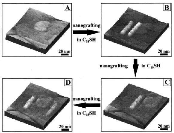
AFM can also be used to remove the monolayer in a solution of replacement thiol 44. Interestingly, the patterns produced by this method (termed ‘nanografting’) form at least one order of magnitude faster and have fewer defect sites than monolayers formed from solution (Fig. 1.5) 45. A wide variety of two component monolayers have been created using nanografting both in situ and ex situ. One interesting example of ex situ patterning was the binding of protein to nanografted areas of mercaptopropionic acid in a dodecanethiolate background 46, 47.
Early studies performed by Xu and Liu 44 utilized the mechanical attributes of AFM in order to displace “matrix monolayer” components from substrates. Through the application of an increase in the force used during scaning, nanoshaving was observed as they had previously reported. However, with the addition of dodecanethiol (C12SH) or
decanethiol (C10SH) in supporting solution it was observed that the replacing “ink” adsorbed
monolayer as well as reform them demonstrated a vast range of control in the selectivity of structural manipulation through AFM 48. Also, structures fabricated through this methodology illustrated control in line resolution, given the reproducible 10 nm line width and 50 nm length. Formation of lines with these dimensions resulted from the application of 5.2 nN setpoint force during the writing scan with 0.1 mM concentration of replacing molecules in 2-butanol solution. In order to confirm the replacement, scans were taken with a reduced 0.3 nN setpoint force. Changes relative height of the replaced region agreed with the difference in lengths of the C18S- and C10S- molecules suggested the complete replacement
of the monolayer in the selected region.
Figure 1.5. (A) An AFM image of C10S SAM prior to fabrication. (B) Patterning of two 10 nm x 50 nm
C18S- lines with 20 nm spacing. (C) Removal of one of the C18S- lines and reintroduction of the C10S- into
the region. (D) Fabricating another C18S- line 65nm in length. Reprinted with permission from [48],
A second classification of substitution lithography is tip induced modification of the terminal head group in the SAM 1. In this process, the underlying chain is left unperturbed with only the chemical functionality of the terminal headgroup affected. STM, AFM and CS-AFM have been used in this process. An interesting example is the chemical modification of an amine terminated organosilane by the low energy electron beam applied to the sample during STM imaging 49. After exposure to the low energy electrons from the STM tip the functionality of the exposed surface was destroyed and therefore would not ligate ions in subsequent steps. The undamaged regions were then exposed to aqueous Pd+2 followed by ex situ exposure to an electroless nickel plating bath. The Pd+2 was bound only to the unexposed regions and the nickel plated only on the Pd+2 regions 49.
In another example, CS-AFM was used to induce an nanoelectrochemical oxidation of the terminal methyl group of a n-octadecyltrichlorosilane monolayer 50. After oxidation of the terminal methyl group, the sample was reacted with a vinyl terminated silane which created a bilayer in the oxidized region. The vinyl group could then be reacted to form various other terminal groups and further layers or functionalities could be added. These examples indicate that substitution lithography on SAMs is another useful method along with addition lithography and elimination lithography in preparing and manipulating the components at a monolayer substrate interface.
1.5 Apparent Height
and height differences several factors contribute towards providing clear-cut responses including the length and relative tilt of the molecules in the replaced region, and how the relative conductance of the tip-molecule-substrate junction varies with applied bias.
Bias dependent apparent height contrast is based upon molecules having a nonlinear increase in tunneling current as the tip-sample bias is increased. Gorman et al. 41 demonstrated that a ferrocenyl-terminated SAM region shows little or no apparent height contrast with the background dodecanethiolate SAM at a 150 mV setpoint bias. However, if the bias was increased to 1000 mV then the ferrocenyl-terminated regions appeared much taller than the C12 background (Fig. 1.6).
The mechanism behind this apparent height contrast is suggested to be resonant tunneling 51. Resonant tunneling occurs when the Fermi energy levels in the tip and a suitable level of the redox active molecule come into alignment. At low potentials the Fermi level of the tip is too low to access a molecular orbital associated with the molecule and therefore little excess tunneling current is observed. However if the Fermi level of the tip is brought
Figure 1.6. Replacement lithography images showing an FcC11SH molecules replaced into a C12
into alignment with a MO on the molecule the tunneling current increases dramatically andan apparent height difference is seen between the insulating background and the electroactive molecule. This effect has been modulated by installing the electroactive groups reversibly using non-covalent interactions 52 and by capping the electroactive group (in this case, binding the ferrocenyl groups with β-cyclodextrin) 53.
The ability to characterize SPL fabrication relies on the interpretation of the surface features formed during the process. In an attempt to characterize the process of replacement lithography, Lewis and Gorman characterized the efficacy of replacement (Fig 1.7) based on the apparent height response 54. In doing so, the establishment of visible and measurable desorption trends based on the length of the initial monolayer were established.
1.6 Concluding Thoughts
Figure 1.7. A series of replacement lithography experiments imaged by STM with FcC11S- as
1.7 References
1. S. Kramer, R. R. Fuierer and C. B. Gorman, Chemical Reviews 103 (11), 4367-4418 (2003).
2. H. T. Soh, K. W. Guarini and C. F. Quate, Scanning Probe Lithography. (Kluwer Academic Publishers, Boston, 2001).
3. C. B. Ross, L. Sun and R. M. Crooks, Langmuir 9 (3), 632-636 (1993).
4. J. K. Schoer, C. B. Ross, R. M. Crooks, T. S. Corbitt and M. J. Hampdensmith, Langmuir 10 (3), 615-618 (1994).
5. J. K. Schoer, F. P. Zamborini and R. M. Crooks, Journal of Physical Chemistry 100
(26), 11086-11091 (1996).
6. J. K. Schoer and R. M. Crooks, Langmuir 13 (8), 2323-2332 (1997).
7. M. J. Lercel, G. F. Redinbo, H. G. Craighead, C. W. Sheen and D. L. Allara, Applied Physics Letters 65 (8), 974-976 (1994).
8. G. Y. Liu and M. B. Salmeron, Langmuir 10 (2), 367-370 (1994). 9. I. Touzov and C. B. Gorman, J. Phys. Chem. B 101, 5263-5276 (1997).
10. S. O. Kelley, J. K. Barton, N. M. Jackson, L. D. McPherson, A. B. Potter, E. M. Spain, M. J. Allen and M. G. Hill, Langmuir 14 (24), 6781-6784 (1998).
11. D. J. Zhou, K. Sinniah, C. Abell and T. Rayment, Langmuir 18 (22), 8278-8281 (2002).
12. J. W. Zhao and K. Uosaki, Langmuir 17 (25), 7784-7788 (2001).
13. D. J. Wold and C. D. Frisbie, Journal of the American Chemical Society 123 (23), 5549-5556 (2001).
14. D. J. Wold and C. D. Frisbie, Journal of the American Chemical Society 122 (12), 2970-2971 (2000).
16. A. M. Rawlett, T. J. Hopson, L. A. Nagahara, R. K. Tsui, G. K. Ramachandran and S. M. Lindsay, Appl. Phys. Lett. 81 (16), 3043-3045 (2002).
17. H. Sugimura, K. Okiguchi, N. Nakagiri and M. Miyashita, J. Vac. Sci. Technol. B 14
(6), 4140-4143 (1996).
18. H. Sugimura and N. Nakagiri, Langmuir 11 (10), 3623-3625 (1995).
19. J. W. Zheng, Z. H. Zhu, H. F. Chen and Z. F. Liu, Langmuir 16 (10), 4409-4412 (2000).
20. Q. G. Li, J. W. Zheng and Z. F. Liu, Langmuir 19 (1), 166-171 (2003).
21. S. M. Kim, S. J. Ahn, H. Lee and E. R. Kim, Ultramicroscopy 91 (1-4), 165-169 (2002).
22. M. Ara, H. Graaf and H. Tada, Appl. Phys. Lett. 80 (14), 2565-2567 (2002).
23. Y. N. Xia, M. Mrksich, E. Kim and G. M. Whitesides, Journal of the American Chemical Society 117 (37), 9576-9577 (1995).
24. Y. Koide, M. W. Such, R. Basu, G. Evmenenko, J. Cui, P. Dutta, M. C. Hersam and T. J. Marks, Langmuir 19 (1), 86-93 (2003).
25. Y. Jun, D. Le and X. Y. Zhu, Langmuir 18 (9), 3415-3417 (2002).
26. P. T. Hurley, A. E. Ribbe and J. M. Buriak, Journal of the American Chemical Society 125 (37), 11334-11339 (2003).
27. D. S. Ginger, H. Zhang and C. A. Mirkin, Angewandte Chemie-International Edition
43 (1), 30-45 (2004).
28. R. D. Piner and C. A. Mirkin, Langmuir 13 (26), 6864-6868 (1997).
29. S. H. Hong, J. Zhu and C. A. Mirkin, Langmuir 15 (23), 7897-7900 (1999). 30. R. D. Piner, J. Zhu, F. Xu, S. Hong and C. Mirkin, Science 283, 661-663 (1999). 31. S. H. Hong, J. Zhu and C. A. Mirkin, Science 286 (5439), 523-525 (1999).
32. F. L. Liu X., Hong S., Dravid V. P., Mirkin C. A., Adv. Mater. 14 (3), 231-234 (2002).
34. J. C. Smith, K. B. Lee, Q. Wang, M. G. Finn, J. E. Johnson, M. Mrksich and C. A. Mirkin, Nano Lett. 3 (7), 883-886 (2003).
35. S. Rozhok, R. Piner and C. A. Mirkin, J. Phys. Chem. B 107 (3), 751-757 (2003). 36. P. V. Schwartz, Langmuir 18 (10), 4041-4046 (2002).
37. P. E. Sheehan and L. J. Whitman, Phys. Rev. Lett. 88 (15) (2002).
38. C. B. Gorman, R. L. Carroll, Y. F. He, F. Tian and R. Fuierer, Langmuir 16 (15), 6312-6316 (2000).
39. F. P. Zamborini and R. M. Crooks, Journal of the American Chemical Society 120
(37), 9700-9701 (1998).
40. P. S. Weiss, L. A. Bumm, T. D. Dunbar, T. P. Burgin, J. M. Tour and D. L. Allara, Ann. N. Y. Acad. Sci 852, 145-168 (1998).
41. C. B. Gorman, R. L. Carroll and R. R. Fuierer, Langmuir 17 (22), 6923-6930 (2001). 42. R. R. Fuierer, R. L. Carroll, D. L. Feldheim and C. B. Gorman, Advanced Materials
14 (2), 154-+ (2002).
43. J. W. Zhao and K. Uosaki, Nano Lett. 2 (2), 137-140 (2002). 44. S. Xu and G. Y. Liu, Langmuir 13 (2), 127-129 (1997).
45. S. Xu, P. E. Laibinis and G. Y. Liu, Journal of the American Chemical Society 120
(36), 9356-9361 (1998).
46. M. E. Browning-Kelley, K. Wadu-Mesthrige, V. Hari and G. Y. Liu, Langmuir 13
(2), 343-350 (1997).
47. K. Wadu-Mesthrige, S. Xu, N. A. Amro and G. Y. Liu, Langmuir 15 (25), 8580-8583 (1999).
48. S. Xu, S. Miller, P. E. Laibinis and G. Y. Liu, Langmuir 15 (21), 7244-7251 (1999). 49. C. R. K. Marrian, F. K. Perkins, S. L. Brandow, T. S. Koloski, E. A. Dobisz and J. M. Calvert, Appl. Phys. Lett. 64 (3), 390-392 (1994).
50. R. Maoz, E. Frydman, S. R. Cohen and J. Sagiv, Advanced Materials 12 (10), 725-+ (2000).
52. G. M. Credo, A. K. Boal, K. Das, T. H. Galow, V. M. Rotello, D. L. Feldheim and C. B. Gorman, Journal of the American Chemical Society 124 (31), 9036-9037 (2002).
53. R. A. Wassel, G. M. Credo, R. R. Fuierer, D. L. Feldheim and C. B. Gorman, J. Am. Chem. Soc. 126, 295-300 (2004).
Chapter 2
Scanning Tunneling Microscope-Based
Replacement Lithography on Self-Assembled
Monolayers. Investigation of the Relationship
Between Monolayer Structure and
Replacement Bias
2.1 Impetus
In this chapter, the effect of the structure of the initial self assembled monolayer on the surface on the replacement lithography process is investigated. The scheme for this process is thought to initially involve localized desorption, followed by replacement by a second component in solution.1 Given this scheme, the degree of replacement at a given bias likely correlates with the relative ease of the desorption step.
2.2 Results and Discussion
Ferrocenyl-undecanethioactetate (Fc-C11SAc) was used as the replacement molecule
because it has been shown to have a considerable height contrast against the insulative background of the methyl terminated monolayers. 2,3 As mentioned previously height contrast is caused by an increased current flow through the molecule which forces the tip to pull away from the surface to reestablish the set point current. The set point current is the user defined current the feedback maintains between the tip and surface. The typical set point current used in these experiments is 10 picoamperes which has been calculated to hold the tip just above the monolayer at the biases (1 volt) used for these experiments.4
As the chain length of an n-alkanethiolate self assembled monolayer increases, a higher bias is required to electrochemically desorb it from gold.5-16 As stated previously it is not clear that replacement lithography operates via an electrochemical desorption mechanism, although it seemed likely that this process would follow the same trend. Upon a
A B
C D
given self assembled monolayer, the tip scanned a series of lines at incrementally higher applied biases. This process was repeated several times on different samples. Typical results are shown in figure 2.2.
In Figure 2.2, the replaced regions appear brighter than the background CnS-self
assembled monolayer regions (where n is the number of carbons (8,10,12,14) of the alkylthiol used initially to compose the self assembled monolayer). The typical line width
produced was similar for the different monolayers used (ca. 12 nm). However, the applied bias required to affect replacement increased with the chain length of the initial monolayer. Thus, if 50% replacement is arbitrarily picked to be considered the onset of replacement then replacement was initiated at a bias of 2.8 V upon an octanethiolate self assembled monolayer. However, the process did not commence until a bias of 3.0 V was used upon a tetradecanethiolate self assembled monolayer (Figure 2.3). This behavior was consistent with difficulty of desorption scaling with the chain length of the monolayer.
Figure 2.3. Graph indicating the percentage of replacement for different CnS-SAMs (n is the number of carbons in the alkylthiol of the initial self assembled monolayer). T bars are drawn to aid in ascertaining the replacement bias required to affect 50% replacement. Error bars are at the 90% confidence interval. Lines are drawn through the points solely as a guide to the eye.
2.4 2.5 2.6 2.7 2.8 2.9 3.0 3.1 3.2 3.3 0 25 50 75 100 -SC 14 -SC12 -SC10 Bias(Volts) -SC8 P e rc e n t R e p la c e m e n t
2.4 2.5 2.6 2.7 2.8 2.9 3.0 3.1 3.2 3.3 0
25 50 75
100 2.4 2.5 2.6 2.7 2.8 2.9 3.0 3.1 3.2 3.3 0
25 50 75
100 2.4 2.5 2.6 2.7 2.8 2.9 3.0 3.1 3.2 3.3 0
The change in bias required for desorption (~35 mV per methylene unit if one considers the onset of the process) is larger than that observed for electrochemical desorption of a series of methyl-terminated self assembled monolayers (circa 15 mV per methylene unit).15,17 This result is, however, not unexpected particularly if the STM tip-induced desorption is electrochemical in nature. Desorption here is occurring in a much less polar environment (dodecane with some available water due to the controlled humidity) than found in the electrolyte solution in the electrochemical experiment. Indeed it has been shown that the polarity of the solvent can increase the difficulty of desorption (~1.6 V for dodecanethiolate in DMF and ~1.8 in ACN Vs ~1.0 in ethanolic KOH) even in electrochemical cells.8,15
At intermediate biases, the process of replacement lithography is not an “all or nothing” process. Thus, the percentage of replacement versus applied bias was determined and graphed as described in the experimental section. These data are shown in Figure 2.3. The error bars indicate the 90% confidence intervals of the mean value. From both figures 2.2 and 2.3 one can distinguish a steady increase in the applied bias required to initiate and to complete replacement. Interestingly, in the case of C8S-SAM, although the minimum bias
The type of group at the terminus of the self assembled monolayer was also hypothesized to influence the desorption and subsequent replacement behavior. Self assembled monolayers with carboxylic acid terminal groups are, for example, known to desorb electrochemically at a lower bias than the analogous monolayers with methyl terminal groups.15,17,19 The degree of order in the monolayer and electrostatic repulsion between polar and/or charged terminal groups are likely influencing factors in this process. To determine the bias dependence of replacement lithography on self assembled monolayers composed of differing terminal groups, this process was studied on monolayers composed from mercaptoundecanol (HOC11SH), mercaptoundecanoic acid (HO2CC10SH) and cyano
decanethiol (NCC10SH). The results are shown in Figure 2.5.
The process of replacement began at a lower bias than that observed for the n-alkanethiolate monolayer of similar chain length. However, the replaced lines are clearly much more diffuse. This result indicates that the extent of replacement was not as complete, and the line-widths observed were wider. Moreover, higher concentrations of thiol in the
dodecane solution were required for replacement (a circa. 70 fold greater concentration of Fc-C11SAc was employed in these experiments compared to those on n-alkanethiolate self
assembled monolayers). In addition, it was much more difficult to reproduce these data. The images shown in Figure 2.5 represent the best from among at least 60 trials. In contrast, replacement lithography on n-alkanethiolate self assembled monolayers was reproducible in the vast majority of trials.
Figure 2.5. A series of STM images in which replacement lithography was attempted at incrementally higher biases on the self assembled monolayers indicated to the left of each image. The numbers above each line represent the applied bias used to effect replacement in that line region. Imaging Conditions: z-scale = 3 nm; relative humidity = 55% ± 2 %; imaging bias = 1.25 V for ‑SC10CN and ‑SC10CO2H and 1.5 V for ‑SC11OH; setpoint
The results shown in Figure 2.5 are rationalized based on three structural features of these self assembled monolayers. First, the degree of order in these self assembled monolayers is lower than that of n-alkanethiolate self assembled monolayers.18 Lower order would plausibly make it easier to initiate desorption, however much like the octanethiolate self assembled monolayer it is possible that the molecules on the edge of the desorbed region lean into the replaced region. The polarity of the terminal groups on these molecules might increase their affinity for the gold surface increasing the number of possible “blocking” molecules. If this is indeed the case it would explain the necessity for increasing the Fc-C11SAc concentration to initiate replacement. The diffuse nature of the lines can then be
explained as a direct result of the higher Fc-C11SAc concentration. Second, it is possible that,
upon desorption, thiols with polar terminal groups aggregate in the nonpolar dodecane, and this aggregation could prevent them from efficiently vacating the local region around which they had been desorbed.
observation is also consistent with the polar terminal groups in these self assembled monolayers facilitating the availability of water at the monolayer/dodecane interface more efficiently than for n-alkanethiolate self assembled monolayers.
2.3 Conclusions
From these data, it is concluded that the structure of a self assembled monolayer strongly influences the process of replacement lithography. Specifically, longer, presumably more well ordered monolayers required a higher applied bias to undergo replacement. Conversely, shorter monolayers and monolayers with cyano-, hydroxyl-, and carboxylic acid terminal groups can undergo replacement at lower applied bias. However, this latter class of self assembled monolayers underwent replacement to a lesser degree of completion and with a poorer resolution. Thus, from the standpoint of high-resolution lithography, well-packed self assembled monolayers have a benefit even if they require a slightly higher bias to perform the operation.
2.4 Experimental
Octanethiol (C8SH), decanethiol (C10SH), dodecanethiol (C12SH), mercaptoundecanol
(HOC11SH) and mercaptoundecanoic acid (HO2CC10SH) were obtained from Aldrich and
used without further purification. Tetradecanethiol (C14SH) was obtained from Fluka and
used without further purification. The cyano decanethiol (NCC10SH) was available from
previous studies and was used without further purification.1 All replacement lithography was performed at relative humidity of 55% ± 2% as maintained by a hydrated dinitrogen flow. The concentration of the undecyl ferrocenyl-thioacetate (FcC11SAc) used to replace regions
of various n-alkanethiolate self assembled monolayers was ca. 6 µM. The concentration of FcC11SAc used to replace regions on self assembled monolayers with non-methyl terminal
groups (e.g. CN, OH, and COOH) was ca. 430 µM.
2.5 References
(1) Carroll, R. L.; Gorman, C. B. Angew. Chem., Int. Ed. 2002, 41, 4379-4400. (2) Gorman, C. B.; Carroll, R. L.; Fuierer, R. R. Langmuir 2001, 17, 6923-6930.
(3) Kramer, S.; Fuierer, R. R.; Gorman, C. B. Chemical Reviews 2003, 103, 4367-4418. (4) Weiss, P. S.; Bumm, L. A.; Dunbar, T. D.; Burgin, T. P.; Tour, J. M.; Allara, D. L. In Molecular Electronics: Science and Technology; NEW YORK ACAD SCIENCES: New
York, 1998; Vol. 852, pp 145-168.
(5) Walczak, M. M.; Popenoe, D. D.; Deinhammer, R. S.; Lamp, B. D.; Chung, C. K.; Porter, M. D. Langmuir 1991, 7, 2687-2693.
(6) Widrig, C. A.; Chung, C.; Porter, M. D. J. Electroanal. Chem. 1991, 310, 335-359. (7) Weisshaar, D. E.; Lamp, B. D.; Porter, M. D. J. Am. Chem. Soc. 1992, 114, 5860-5862.
(8) Schneider, T. W.; Buttry, D. A. J. Am. Chem. Soc. 1993, 115, 12391-12397.
(9) Imabayashi, S.; Iida, M.; Hobara, D.; Feng, Z. Q.; Niki, K.; Kakiuchi, T. J. Electroanal. Chem. 1997, 428, 33-38.
(10) Yang, D. F.; Wilde, C. P.; Morin, M. Langmuir 1997, 13, 243-249.
(11) Kawaguchi, T.; Yasuda, H.; Shimazu, K.; Porter, M. D. Langmuir 2000, 16, 9830-9840.
(12) Ma, F. Y.; Lennox, R. B. Langmuir 2000, 16, 6188-6190.
(13) Vinokurov, I. A.; Morin, M.; Kankare, J. J. Phys. Chem. B 2000, 104, 5790-5796. (14) Wong, S. S.; Porter, M. D. J. Electroanal. Chem. 2000, 485, 135-143.
(15) Kakiuchi, T.; Usui, H.; Hobara, D.; Yamamoto, M. Langmuir 2002, 18, 5231-5238. (16) Sumi, T.; Wano, H.; Uosaki, K. J. Electroanal. Chem. 2003, 550, 321-325.
(17) Gyepi-Garbrah, S. H.; Silerova, R. Phys. Chem. Chem. Phys. 2001, 3, 2117-2123. (18) Besenbacher, F. Rep. Prog. Phys. 1996, 59, 1737-1802.
Chapter 3
The Utilization of Replacement Lithography to
Create Nanostructures of Various Ferrocenyl
Terminus Alkanethiols with and without β
Ketone on Au (111) and Studied via Scanning
3.1 Introduction
In recent years, the field of molecular electronics has enjoyed a fair amount of interest due in some part to the limitations inherent in the current computer chip manufacturing industry1 This interest is also driven by the idea that molecular electronics is the ultimate in miniaturization of electronic devices1, 2 . There has been progress made towards the creation of a molecular transistor device, and there have been a myriad of experiments performed with a multitude of different molecules towards this end. However, despite these advances, there still is a fair amount that is not understood about the mechanisms that govern the behavior of these assemblies.
A classic example of this uncertainty is manifest in the phenomenon known as negative differential resistance (NDR) which can be defined as being a decrease in the current with an increasing bias as is illustrated in the blue box region of Figure 3.1. While there have been several mechanisms proposed for this process, there is still not a clear winner3-26. Furthermore, our understanding of what is necessary to facilitate an NDR event is also not well understood. While previously efforts have been made by members of the Gorman group to determine the effect of chain length or redox potential on the NDR process, their work was unfortunately stymied by the less than cooperative nature of the experiment27,
28
A multitude of different techniques can be utilized to determine how both changes in the redox potential and the chain length of the molecule being interrogated affect its conductivity. These generally vary as to how the molecule is “wired up” or contacted by two electrodes. Prior reports utilized nanopores8, 29, conductive probe atomic force microscopy (AFM)7, 19, 30, scanning tunneling microscopy (STM)15, 17, 25, 27, 31, 32, and other techniques to accomplish the goal of probing molecular species33-35. For the work summarized here, however, we focused on the use of the scanning tunneling microscope (STM) to further our understanding at the molecular scale.
In this work, we seek to understand how the change in the redox potential and the variance in the chain length affect the conductivity of the ferrocene moiety in a metal-molecule-metal junction. Earlier attempts at trying to pin down a direct correlation between the redox potential of a molecule and the bias at which NDR takes place suffered from a
V
I
large variability in the peak potential of the NDR event15, 19, 27, 28. Therefore, it was determined that it would be best if we could stay away from using a Scanning Tunneling Spectroscopy (STS) type of approach. STS utilizes a predetermined pattern 1024 points of measurement. In this technique the tip will move to a predetermined spot and then current versus voltage curve is collected. This process is repeated for a grid of points on the surface. It is assumed that the main cause for the large variation in the peak potential seen in NDR stems from the molecules being interrogated constantly “seeing” a different tip28
. If one considers the interrogation of a molecule to be its interaction with the apex of the STM tip, then it is clearly difficult or impossible to bring the tip into exactly the same relative orientation with a molecule repeatedly as one scans across a surface. The process is further complicated by the bulky ferrocenyl terminus creating a disordered monolayer which could allow for some movement of the molecules on the surface36. The constant change in the local density of states that the molecule could experience when interacting with the tip in these different geometries provide plenty of possible scapegoats for the lack of a consistent data when collected in this manner.
high rate of speed, circa 1900 nm/s, we hypothesize that the resultant data should have less variation.
The hypothesis that an increase in the scan speed would cause a decrease in the variation might seem counterintuitive; however, it is based on using the scan speed to “outrun” thermal drift inherent in all piezo electric scanners. If the tip is parked over a relatively small area for an extended period of time, or if a slow scan rate is utilized, then the amount of thermal drift from the piezo can cause the tip to molecule sample distance to vary while interrogating the molecule. However if a sufficiently fast scan time is used it may be possible to measure the instantaneous current at the tip to molecule interface without introducing thermal drift instabilities into the equation and even though the utilization of constant current mode does cause the tip to sample distance to vary that variance should average out over the thousands of molecules probed to give a consistent data set.
3.2 Methods
Desorbed Thiol
Replacement Thiol
Dodecane Layer
Au(111)
Desorbed Thiol
Replacement Thiol
Dodecane Layer
Au(111)
3.3 Premise
It was hypothesized that as the chainlength of the ferrocene terminus thiolate was decreased the overall apparent height of the molecule would increase. The basis was predicated on the following: as the alky chain is increased its corresponding resistance to electrochemical desorbtion both utilizing an electrochemical cell40, 41 and while using an STM is increased39, 42. Since the later has been shown to be correct, one could also surmise that there would be a greater resistance to transconductance as well. This led into the hypothesis that a shorter chainlength between the ferrocene terminus and the thiolate binding
Ferrocenyl-undecanethiol (Fc-C11SH)
Fe
SH
Fe
SH
Ferrocenyl-hexanethiol (Fc-C6SH)
Fe SH O Ferrocenyl-6-hexanonethiol Fe O SH Ferrocenyl-11-undecanonethiol
Ferrocenyl-undecanethiol (Fc-C11SH)
Fe
SH
Fe
SH
Ferrocenyl-hexanethiol (Fc-C6SH)
Fe SH O Ferrocenyl-6-hexanonethiol Fe O SH Ferrocenyl-11-undecanonethiol
Figure 3.3. Structure of the replacement inks used. Herein Ferrocenyl undecanethiol will be referred to as FcC11 Ferrocenyl hexanethiol as FcC6 Ferrocenyl-11-undecanonethiol as FcCOC10 and
group should afford a decrease in resistance. Which in turn would lead to increased transconductance which would be seen as an overall increase in the apparent height of that molecule. An initial experiment was setup and executed, with the method explained below, and the results were promising illustrating an increased apparent height for the shorter molecule that was used, FcC6S-, versus the longer, FcC11S-, molecule. Since our initial tests
were so positive we decided to broaden out our scope and look not only molecules with shorter connecting alkyl chains but also at molecules with substituents which affected the ferrocene's electrochemical redox potential. The molecules that we chose, as mentioned previously Figure 3.3, were two whose overall length were the same as the aforementioned choices so we could compare both how the length and the redox potential affected their apparent height.
One of the pathways for electron tunneling from the tip to the substrate in STM is thought to be through the HOMO or LUMO of the molecules on the surface27. With this in mind we determined that if a molecule with an accessible HOMO or LUMO could be utilized then it should illustrate a greater transconductance than a similar molecule where those same orbitals were not accessible. By utilizing the redox potential of a molecule it is possible to locate where the HOMO of that molecule would lie43. Figure 3.4 below illustrates that for both the molecules that we chose.
Figure 3.4 shows the Fermi levels for both the alkane thiol covered gold surface (6.3 electron volts (eV)44 at 0 bias 6.8 eV at 1 V) and the that of the Platinum/Iridium tip (5.6 eV45 at 0 bias 5.1 eV at 1 V) at both a bias of zero and a sample bias of +1 V. This diagram shows that the HOMO of the FcCH2 species is around 5.5 electron volts (eV)46 where the
FcCO HOMO is around 5.75 eV. This is because the electrochemical redox potential of FcCOC10S- had been previously measured28 and was known to be 250 millivolts (mV) higher
than FcC11S- which in turn means it is harder to oxidize than FcC11S- therefore on this scale
So our initial hypotheses are that because of the location of the FcCO HOMO the apparent height of those molecules should be less than that of Fc(CH2)n at low bias and that the
apparent height of the shorter ferrocenyl terminated molecules will be greater than that of the longer ferrocenyl terminated counterparts.
3.4 Results and Discussion
As previously mentioned the first experiment done was to test the hypothesis that as the chainlength decreased the apparent height would increase on a ferrocenyl terminated alkanethiol. This was done by attempting to create nanostructures of two different chainlength ferrocene moieties in close proximity on a surface so that it would be easy to
Figure 3.4) The gold lines represent the Fermi levels for the substrate 6.3 eV and the gray lines for the tip 5.6 eV in the theoretical metal molecule metal junction while the red lines represent the HOMO of the FcCO(CH2)n species 5.75 eV and the blue lines represent the Fc(CH2)n species 5.5 eV and the dashed line represents the Fermi level of the Normal Hydrogen Electrode (NHE). The diagram on the left shows the metal-molecule-metal junction at a bias of 0V where the diagram on the right illustrates the same junction bias of +1V. In this particular junction the tip, which is negatively charged, shifts its Fermi level down and the sample, which is positive, shifts its Fermi level up.
4.0
4.5
5.0
5.5
6.0
6.5
7.0
7.5
Au-S Pt FcCH2 HOMO FcCO HOMOAt 0 V
4.0
4.5
5.0
5.5
6.0
6.5
7.0
7.5
Au-S Pt FcCH2 HOMO FcCO HOMOAt 1 V
N.H.E
N.H.E
determine at various biases if the molecules had different apparent heights and therefore different current passing capabilities. This was accomplished by first creating a nanostructure on the surface with ferrocenylhexane thiol. After a nanostructure that was suitable had been created the scanner was retracted a small amount. Then the sample was rinsed with fresh dodecane a minimum of five times via removing and then replacing the dodecane in the cell as represented in Figure 3.5.
Fresh dodecane was added to the cell and the scanner was engaged with the surface. The previously created nanostructure was then relocated. Then the second ink was carefully added to the cell while scanning. After adding the second ink a second nanostructure was created in close proximity to the first nanostructure and then several scans were taken over the patterned region at various biases. Figure 3.6 shows the results of one experiment.
A
B
C
A
B
C
In Figure 3.6A the top nanostructure is Ferrocenyl-undecanethiolate and the lower nanostructure is Ferrocenyl-hexanethiolate. Figure 3.6B is a line of the nanostructures and clearly illustrates that the Ferrocenyl-hexanethiolate has a taller apparent height contrast compared to the Ferrocenyl-undecanethiolate. While this experiment does an excellent job of clearly demonstrating that the Ferrocenyl-hexanethiolate nanostructure has a higher apparent contrast it does not lend itself well to multiple repetitions and therefore it we created homogenous nanostructures of each of the ferrocene derivatives illustrated in Figure 3.5. This trend of decreasing chain length corresponding to an increase in the apparent height is clearly visible in Figure 3.6 where the FcC6 molecule has a greater apparent height than
FcC11.
In order to more fully understand this phenomenon it was proposed that a study be done utilizing the molecules illustrated in Figure 3.3 however in this study instead of
A
B
FcC11
FcC6
A
B
FcC11
FcC6
comparing multiple inks at once we would instead create nanostructures utilizing replacement lithography and then interrogate those structures at various bias in order to determine how their apparent height would change over a bias range and how that apparent height would differ between molecules containing a ketone species and those without. The results of these studies are illustrated in Figure 3.7
0.6 0.8 1.0 1.2 1.4
0.0 0.1 0.2 0.3 0.4 0.5 0.6 0.7 0.8
FcC11S-Au
Bias (V) 0.0 0.1 0.2 0.3 0.4 0.5 0.6 0.7 0.8
FcC6S-Au
-0.6 -0.4 -0.2 0.0 0.2 0.4 0.6 0.8
FcC=OC10S-Au
-0.10.0 0.1 0.2 0.3 0.4 0.5 0.6 0.7 0.8
FcC=OC5S-Au
A
p
p
a
re
n
t
H
e
ig
h
t
(n
m
)
Max = 0.35 nm
Min = 0.02 nm
Delta= 0.33 nm
Max = 0.42 nm
Min = -0.42 nm
Delta= 0.84 nm
Max = 0.77 nm
Min = 0.44 nm
Delta= 0.33 nm
Max = 0.80 nm
Min = 0.34 nm
Delta= 0.46 nm
Figure 3.7) An illustration of the apparent height (which is the difference between the registered height of the molecule of interest compared to the background) Vs bias of FcC11S-Au , FcC6S-Au , FcCOC10S-Au, and FcCOC5S-Au. The red lines represent the 95% confidence interval for each point. The error was determined from either a Gaussian or Lorentzian fit of greater than 5000 pixels per point.
Figure 3.7. An illustration of the apparent height (which is the difference between the registered height of the molecule of interest compared to the background) vs the bias of FcC11S-Au, FcC6S-Au, FcCOC10S-Au,
and FcCOC5A-Au. The red lines represent the 95% confidence interval for each point. The error was
determined from either a Gaussian or Lorentzian fit of greater than 5,000 pixels per point. FcC11S-Au 0.80
3.5 Conclusions
As you can see the data that was collected from the aforementioned experiments does seem to follow several of the trends that we had hypothesized with the FcC6S-Au
nanostructures illustrating a higher apparent height when compared to the longer FcC11S-Au
nanostructures throughout much of the bias range that was used. Our other hypothesis that the nanostructures that were created utilizing the FcCOC5S- and the nanostructures utilizing
the FcCOC10S- molecule would illustrate a lower overall apparent height than the non-ketone
molecules does also seem to be correct at low bias however as the bias was increased something strange happened with both the long chain Fc terminus molecules. Both ended up taller than their shorter counterparts, although that difference is negligible between FcC11S-
and FcC6S-. We think the most likely rationale behind this data is due to the shorter chain
structures forming a more disordered system then the longer chainlength systems. It has previously been established that as the chainlength of an alkylthiolate SAM decreases the amount of disorder increases and it is probable that given the relatively short alkylthiolate tether on both the ketone and non ketone species that the nanostructures were more disordered than their longer chainlength counterparts.
Several attempts were made to establish that this was indeed the case however instead of observing an increase in the apparent height the molecule would appear to have been desorbed from the surface. Our explanation is that the since at negative bias the tip is bias positive that the most probable event that occurred was a combination of electrostatic attraction between the tip and the ketone species either present on the surface or in solution and this caused the either the appearance of a desorbed nanostructure or that the nanostructures were indeed desorbed from the surface, similar results have been seen by other groups47 specifically under the conditions that we used.
Figure 3.8) The gold lines represent the Fermi levels for the substrate 6.3 eV and the gray lines for the tip 5.6 eV in the theoretical metal molecule metal junction while the red lines represent the HOMO of the FcCO(CH
2)n species 5.75 eV and the blue lines represent the Fc(CH2)n species 5.5 eV and the dashed line
represents the Fermi level of the Normal Hydrogen Electrode (NHE). The diagram on the left shows the metal-molecule-metal junction at a bias of 0V where the diagram on the right illustrates the same junction bias of -1V. In this particular junction the tip, which is positively charged, shifts its Fermi level up and the sample, which is negative, shifts its Fermi level down.
4.0
4.5
5.0
5.5
6.0
6.5
7.0
7.5
Au-S Pt FcCH2 HOMO FcCO HOMOAt 0 V
4.0
4.5
5.0
5.5
6.0
6.5
7.0
7.5
Au-S Pt FcCH2 HOMO FcCO HOMOAt -1 V
N.H.E
N.H.E
Figure 3.8 The gold lines represent the Fermi levels for the substrate 6.3 eV and the gray lines for the tip 5.6 eV in the theoretical metal molecule metal junction while the red lines represent the HOMO of the FcCO(CH2)n species 5.75 eV and the blue lines represent the Fc(CH2)n species 5.5 eV and the