ISSN 2348 – 7968
Average Current Mode Control Technique Applied to Boost
Converter for Power factor Improvement and THD Reduction
Dhivya A1, Murali D 2
1
EEE, Anna University, Government College of Engineering, Salem, Tamilnadu, India
2
EEE, Anna University, Government College of Engineering, Salem, Tamilnadu, India
Abstract
Power factor has a high impact on power system industries. A load with low power factor draws more current than a load with high power factor for the same amount of useful power transferred. The high current increases the energy lost in the distribution system and requires large equipment to dissipate wasted energy. Electrical utilities usually charge high cost to industrial/commercial consumers where there is a low power factor. With the development of technology in power semiconductors devices, the rate of using power electronics system has expanded to new and wide applications that include residential, commercial, aerospace and other systems. In the non-linear systems, loads are the main sources of harmonics and it affects efficiency. The current dawn by the power electronics interface from the line is distorted resulting in a high total harmonic distortion (THD) and low power factor (PF).This creates adverse effects on the power system that include increased magnitude of neutral current in a three phase system, over heating of transformers and induction motor. Hence, there is a continuous need for both the improvement of power factor and reduction of line current harmonics. This work is to implement a boost converter with average current mode control technique for the improvement of the power factor and reduction of total harmonics distortion. The boost converter can perform this type of active power factor correction in many discontinuous or continuous modes. Average current measurement provides the input current with high degree of accuracy. Average current mode control technique works wells even when the mode boundary is crossed into the discontinuous mode at low current levels. Open and closed loop boost converter using average current mode control has been simulated by power simulation (PSIM) software. Hence the waveforms of the input current shows the improvement of PF and reduction of THD.
Keywords: Average Current Mode Control, Boost Converter, Continuous conduction mode, Diode rectifiers, Electromagnetic interference, Power Factor(PF), PSIM, Total Harmonic Distortion (THD).
1.
Introduction
Single phase diode rectifiers are the most commonly used circuits for application where the input is the ac supply
(e.g.: computers, telecommunications, air conditioning etc). These classical converters operate by rectifying the input ac line voltage and filtering it with large capacitor. The filter capacitor reduces the ripple present in the output voltage but introduces distortion in the input current which reduces the power factor. So PFC techniques are used. Various power factor correction (PFC) techniques are employed to overcome these power quality problems out of which the boost converter topology has been extensively used in various ac/dc and dc/dc applications. In fact, the front end of today’s ac/dc power supplies with power-factor correction (PFC) is almost exclusively implemented with boost topology [2-4]. The low power factor and high pulsating current from the AC mains are the main disadvantages of the diode rectifier and phase controlled rectifier. These circuits generate serious power pollution in the transmission or distribution system. The power pollutants such as reactive power and current harmonics results in line voltage distortion, heating of core of transformer and electrical machines and increasing losses in the transmission and distribution line.
The boost PFC circuit operating in continuous conduction mode (CCM) is the popular choice for medium and high power (400 W to a few kilowatts) application. This is because the continuous nature of the boost converter’s input current results in low conducted electromagnetic interference (EMI) compared to other active PFC topologies such as buck–boost and buck converters. The active rectifier of the AC/DC/AC converter is used to regulate the DC bus voltage for motor drive. The non-linear load produces a pulsating current with large current harmonics [5-6].
ISSN 2348 – 7968
To combine the capabilities of power factor correction, active power filter and AC/DC converter, a new power factor correction technique using PFC Boost converter is proposed to work simultaneously as an active power filter to supply compensated currents that are equal to the harmonic currents \(excitation leading to saturation). A hysteresis current control is adopted to track the required line current command. In this arrangement PFC boost converter can be used to eliminate the harmonic current generated by the diode rectifier.
The PFC boost converter supplies the required harmonic current produced by the non-linear load, hence the total arrangement draws a nearly sinusoidal current with improved power factor [10-12]. In a conventional switching power supply using a buck derived technique, an inductor is used in the output stage. Current control mode is actually output current control, resulting in many performance advantages [11-13].
In contrast, in a high power factor pre-regulator using the boost technique, the inductor is used in the input stage. Current control mode then controls input current, allowing it to be easily followed to the desired sinusoidal wave shape. In high power factor boost pre-regulators the peak/average error is very serious because it causes distortion of the input current waveform. While the peak current follows the desired sine wave current, the average current does not. The peak/average error becomes much worse at lower current levels, especially when the inductor current becomes discontinuous as the sine wave approaches zero in every half cycle.
To achieve low distortion, the peak/average error must be small. This requires use of a large inductor to make the ripple current small. The resulting shallow inductor current ramp makes the already poor noise immunity much worse. The average current mode method can be used to sense and control the current in any circuit branch. Hence it can control input current accurately with buck and fly back techniques, and can control output current with boost and fly back techniques [13,14].This paper initially involves simulation of basic power electronic conventional rectifier circuits and the analysis of the current and voltage waveforms. It starts with simple circuits and switches to advanced circuits by implementing advanced techniques such as active PFC and their subsequent effect on the current and voltage waveforms expecting better results, mainly focusing on the objective of improving the input current waveform i.e. making it sinusoidal by tuning the circuits. Here for average current mode control, PI controllers are used. All the simulation is done by PSIM.
2.
Power Factor With Different Loads
Power factor is defined as the cosine of the angle between voltage and current in an ac circuit. If the circuit is inductive, the current lags behind the voltage and power factor is referred to as lagging. However, in a capacitive circuit, current leads the voltage and the power factor is said to be leading.2.1
Linear System
It is AC electrical loads where the voltage and current waveforms are sinusoidal. The current at any time is proportional to voltage. Power factor is determined only by the phase difference between voltage and current.
2.2 Non Linear System
Applies to those ac loads where the current is not proportional to voltage. The nature of the nonlinear current is to generate harmonics in the current waveform. This distortion of the current waveform leads to distortion of voltage waveform. Under this condition, the voltage waveform is no longer proportional to current. For sinusoidal voltage and non-sinusoidal current PF can be expressed as: θ cos 1 × × × = rms rms rms rms I V I V
PF (1)
p d rms rms K K I I
PF = 1 ×cosθ= × (2)
Where, cosθ is the displacement factor of the voltage and current. Kp is the purity factor or the distortion factor. Another important parameter that measures the percentage of distortion is known as the Total Harmonic Distortion (THD).
3.
Effects Of Harmonics On Power Quality
The contaminative harmonics can decline power quality and affect system performance in several ways. As presence of harmonics declaims the transmission efficiency and also creates thermal problems, both conductor and iron loss are increased. In 3-Φ system, neutral conductor becomes unprotected due to odd harmonics. Triggering is misconducted as the peak harmonics create currents which interrupts the protection system of an automatic relay. Huge current flows through the ground conductor of system with four wire 3-Φ when odd number of n- current is present in harmonics.
ISSN 2348 – 7968
degrading reliability of electrical equipment, increasing product defective ratio, insulation failure, audible noise etc.
4.
Types Of Power Factor Correction
4.1 Passive PFC
Harmonic current can be controlled in the simplest way by using a filter that passes current only at line frequency (50 or 60 Hz). Harmonic currents are suppressed and the non-linear device looks like a non-linear load. Power factor can be improved by using capacitors and inductors. Power factor can be improved by using capacitors and inductors. But the disadvantage is they require large value high current inductors which are expensive and bulky.
4.2 Active PFC
An active approach is the most effective way to correct power factor of electronic supplies. Here, we place boost converter between the bridge rectifier and the load. The converter tries to maintain a constant DC output bus voltage and draws a current that is in phase with and at the same frequency as the line voltage.
5.
Boost Converter
To prevent the problem of pulsating input current PFC techniques are used. Best result can be obtained by using active PFC techniques based on switch mode power converters. The boost topology is by far more popular than other PFC techniques. The circuit diagram of a boost converter is shown in Figure. 1
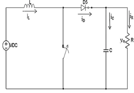
Fig.1 Boost converter
When the switch S is on the current IL rises and flows through inductor L. When switch S is off the current IL decreases and flows through L, diode D5, C, and R. The current IL falls until switch S is turned on again.
So when switch S is on:
L V
t iL in
= ∆ ∆
(3)
Again when the switch is off:
dt di L V
Vin− o= L (4)
Here Vin is the rectified input voltage and Vo is the output voltage. So the boost converter draws continuous input current. This input current can be controlled to follow a sinusoidal reference using average current mode control technique.
6.
Average Current Mode Control
6.1
System specifications
Average current control Boost Converter for the improvement of power factor and total harmonic distortion has been used in this work. The boost converter is a highly efficient step-up DC/DC switching converter. The converter uses a transistor switch, typically a MOSFET, to pulse width modulate the voltage into an inductor. Rectangular pulses of voltage into an inductor result in a triangular current waveform. For this work it is also assumed that the converter is used in the continuous mode, which implies that the inductor's current never goes to zero.
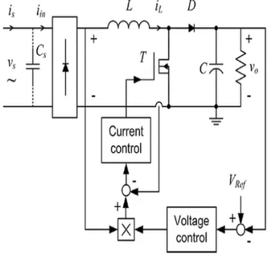
Boost converter has two conduction states, continuous conduction mode and discontinuous conduction mode. The block diagram of boost converter is shown in Figure. 2 The average current mode control method is feedback control for current. It contains two PI controllers to stabilize the system. After using this average current control method the results are good.
ISSN 2348 – 7968
The average current mode control the control circuit consists of two parts. They are:
• Feed forward/current control loop
• Feedback /voltage control loop
6.2. Current Control Loop
The purpose of the current control loop is to force the current waveform to follow the shape of the voltage waveform. In order for the current to follow the voltage, the internal current amplifier has to be designed to capture enough of the harmonics of the output voltage using external capacitors and resistors.Once designing this it uses information from the gain modulator to adjust the PWM control that controls whether the power MOSFET is switched on or off. The heart of the PFC controller is the gain modulator. The gain modulator has two inputs and one output. The left input to the gain modulator block is called the inductor current(IL). The reference current is the input current that is proportional to the input full-wave-rectified voltage. The other input, located at the bottom of the gain modulator, is from the voltage error amplifier. The error amplifier takes in the output voltage (using a voltage divider) after the boost diode and compares it to a reference voltage. The error amplifier will have a small bandwidth so as not to let any abrupt changes in the output or ripple erratically affect the output of the error amplifier. The gain modulator multiplies or is the product of the reference current and the error voltage from the error amplifier (defined by the output voltage).
6.3 Voltage Control Loop
The gain modulator and the voltage control loop work together to sample the input current and output voltage, respectively.
Fig.3. Average current mode control
These two measurements are taken and then compared against each other to determine if a gain should be applied to the input of the current control. This decision is than compared against a sample of the output current to determine the duty cycle of the PWM.
Once designing this it uses information from the gain modulator to adjust the PWM control that controls whether the power MOSFET is switched on or off. The heart of the PFC controller is the gain modulator. The gain modulator has two inputs and one output. The left input to the gain modulator block is called the inductor current (IL). The reference current is the input current that is proportional to the input full-wave-rectified voltage. The other input, located at the bottom of the gain modulator, is from the voltage error amplifier. The error amplifier takes in the output voltage (using a voltage divider) after the boost diode and compares it to a reference voltage. The error amplifier will have a small bandwidth so as not to let any abrupt changes in the output or ripple erratically affect the output of the error amplifier. The gain modulator multiplies or is the product of the reference current and the error voltage from the error amplifier (defined by the output voltage).
7.
Simulation Results And Discussions
7.1 Simple Bridge Rectifier
The circuit diagram of simple bridge rectifier is shown in Figure. 4
Fig.4 Simulation diagram of simple Bridge Rectifier
ISSN 2348 – 7968
Fig.5 Input Current waveform of Simple bridge rectifier
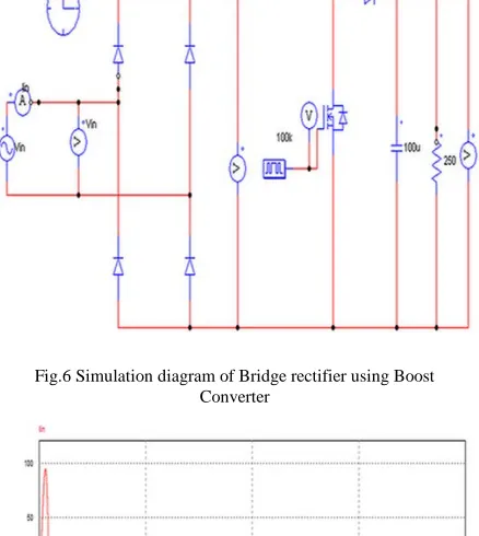
7.2 Bridge Rectifier Using Boost Converter
Fig.6 Simulation diagram of Bridge rectifier using Boost Converter
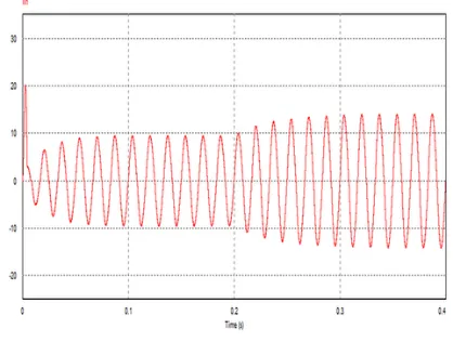
Fig.7 Input Current waveform of Boost Converter
The results of input current are shown in Figure.7. The result shows presence of lot of ripples in the waveform indicating a very high THD.It indicates that THD is more than 60% that needs to be reduced to around 5%. To achieve the desired goal an average current controller using boost converter is designed.
7.3 Average Current Control Method using Boost
Converter
The circuit diagram of Average Current Control method using Boost Converter is shown below in Figure.8. PSIM software is used for the design of circuit. The input voltage for the bridge rectifier is 220VRMS and output voltage of the boost converter is 400V, 500V, 600V, for a Duty cycle of 0.4, 0.5, 0.6 and results are compared whereas values of PI controller are chosen according to the circuit requirements.
Fig .8 Simulation diagram of Average Current Control Method Applied to Boost converter for fixed load
ISSN 2348 – 7968
The simulation results are shown below. The input voltage for the bridge rectifier is shown in Figure.9, which is 220VRMS.Due to boost converter circuit output is higher than the input. The output voltage is 400V DC for duty cycle of 0.4. The output waveform is shown in Figure.10
Fig.10 Output Voltage waveform of average current control method for a duty cycle of 0.4
The Input Current for duty cycle of 0.4 is shown below in Figure.11
Fig.11 Input Current waveform for a duty cycle of 0.4
The waveform shows no presence of ripples, hinting towards a good THD value
Fig.12 Output Voltage waveform of average current control method for a duty cycle of 0.5
The Input Current for duty cycle of 0.5 is shown below in Figure.13
Fig.13 Input Current waveform for a duty cycle of 0.5
Fig.14 Output Voltage waveform of average current control method for a duty cycle of 0.6
ISSN 2348 – 7968
It shows that THD is almost 4.5%, which is considered as a good THD value. So results are improved by applying the average current control method to the Boost Converter. In the average current control method, a feedback circuit diagram has been used which can be seen in Figure.8.
7.4 Average Current Control Method Boost
Converter using Variable Load
The circuit diagram is shown in Figure.16, which shows the Average Current Control Method using variable load. Step size of 0.2 sec is selected while parallel resistance of 500 ohm is selected. It is clear from Figure.23 that after 0.2 sec step output voltage, input current and input voltage goes down to 0.2 and then restore to the original position. The Block diagram of the circuit is shown in Figure.3.
Fig.16 Simulation circuit of Average Current Control Method for Variable Load
The output Voltage for duty cycle of 0.4 is shown in Figure.17
Fig.17 Output Voltage waveform with Variable Load for duty cycle of 0.4
The input current for a duty cycle of 0.4 is shown below in Figure.18 shows the change at 0.2 sec.
Fig.18 Input Current waveform with Variable Load for duty cycle of 0.4
Fig.19 Output Voltage waveform with Variable Load for duty cycle of 0.5
ISSN 2348 – 7968
Fig.21 Output Voltage waveform with Variable Load for duty cycle of 0.6
Fig.22 Input Current waveform with Variable Load for duty cycle of 0.6
After applying the variable load, the THD is shown which is around 4% and considered to be reasonably good.
Table 1. Comparative Analysis Of Result
Duty Cycle
Average Current Controlled Method Applied To Boost Converter For Fixed Load
Average Current Controlled Method Applied to Boost Converter For Variable Load
PF THD(%) PF THD(%)
0.4 0.919 4.674 0.93 4.039
0.5 0.969 3.293 0.96 3.52
0.6 0.985 3.069 0.97 3.23
From the above Table.1, it can be seen that THD value has been improved reasonably by average current controlled method technique.
8.
Conclusion
THD and PF correction of Boost Converter using Average current control method is presented in this thesis. PSIM software has been used for circuit design, measurement of THD and PF. Initially results of open loop uncontrolled rectifier are shown, followed by description of the average current control method. The average current control method resulted in enhancement of the performance and improvement of the results (THD and PF).In the results of uncontrolled rectifier, it can be seen that harmonics are very high. Closed loop controlled rectification is then used for harmonics reduction and PI controllers were tuned to get the satisfactory results. The comparison of Inductor current and the reference current is also presented which is essential for the comparison of rectified scaled voltage and the output DC voltage. Furthermore the transient and steady state analysis of average current control method is also given, which shows satisfactory results. In the end an improved THD value of 4.45% is achieved using simulation.
References
[1] Habib, Aftab Alam, Shahbaz Khan, Rooh ul Amin, and Syed M Ali, “Average current mode control boost converter for the tuning of total harmonic distortion and power factor correction using PSIM,”Journal of Electrical Engineering, Vol.15,March 2015,pp. 287-293.
[2] J.T.Boys, A.W.Green, “Current-forced single-phase reversible rectifier,” IEE Proc. B 136, Vol.3, pp. 205-211 [3] S.Manias, “Novel full bridge semi-controlled switch mode
rectifier,” IEE Proc. B 138, Vol. 3, 1991,pp. 252-256. [4] R.Martinez, P.N.Enjeti, “A high-performance single-phase
rectifier with input power factor correction,” IEEE Trans. PE 11, Vol. 2, 1996, pp. 311-317.
[5] J.P.M Figueiredo, F.L.Tofoli and Silva A. Bruno Leonardo Silva, “A Review of Single-Phase PFC Topologies Based on The Boost Converter,” IEEE Trans. IA, 2010, pp. 1-6. [6] L.Rossetto, G.Spiazz, “Control techniques for power factor
correction converters,” in Proc.Power Electronics, Motion Control (PEMC), September 1994, pp. 1310–1318. [7] K.M.Smedley and S.Cuk, “One-cycle control of switching
converters,” IEEE Trans.Power Electronics, Vol. 10, no. 6, pp. 625–633, November 1995.
[8] D.Borgonovo, J.P. Remor, I.Barbi, and A.J.Perin, “A self-controlled power factor correction single-phase boost pre-regulator,” in Proc .IEEE 36th Power Electronics Specialists Conference (PESC '05), 2005, pp. 2351–2357.
[9] B.R.Lin, “A Single-phase three-level pulsewidth modulation AC/DC converter with the function of power factor corrector and active power filter,”Electric Power Systems Research 58, 2001, pp. 157–167.
[10]P.Karuppanan,Kamala Kanta mahapatra, “PI and fuzzy logic controllers for shunt active power filter,”ISA Transactions 51, 2012, pp. 163–169. Iigure
ISSN 2348 – 7968
Industrial Electronics and Applications, 3rd IEEE Conference, 2007, pp.2199–2204.
[12]C.Morel, P.Yang, Y.Liu and J.Deng, “Application of Slide Mode Control to a Current-Mode-Controlled Boost Converter,” IECON 28th Annual Conference of the Industrial Electronics Society,Vol no. 50407017, 2012, pp. 2199–2204.
[13]S.Kolluri, “Analysis, Modeling, Design and Implementation of Average current mode control for interleaved boost converter,” Power Electronics and Drive Systems (PEDS), IEEE 10th International Conference, no. 4, 2013,pp. 280– 285.