ABSTRACT
SARKAR, BIPLAB. Atomic Layer Deposition (ALD) Enabled Techniques for Novel Memory Applications. (Under the direction of Dr. Veena Misra.)
Moore’s law has resulted in the aggressive scaling of both logic and memory devices. Al-though the memory performance has been greatly improved as a result of scaling, but the volatile memory and non-volatile memory still take two different areas in a circuit. Tradition-ally, permanent data such as codes, look-up tables, etc. are stored in the non-volatile memory segment of the processor. On the other hand, volatile memories are used to perform logical op-erations. A significant advantage in circuit area can be achieved if the two memory technologies are combined in the same device. Such a device can potentially provide higher processing speed, and require simpler circuit architecture for accessing the memory elements. The device can also be potentially attractive for applications like instant ON computing, neuromorphic systems, sensor systems, etc.
In this dissertation, novel concepts of unified memory devices have been discussed which can combine the volatile and non-volatile operation in a single transistor. A dual floating gate mem-ory MOSFET has been demonstrated to show simultaneous volatile and non-volatile operation. The device structure is very similar to a flash memory, but have an additional floating gate. The gate stack of the device consists of a thin dielectric separating two floating gates sandwiched between a tunnel dielectric and inter-poly dielectric. Depending upon the bias applied at the gate of the transistor, the device can be programmed into volatile mode, non-volatile mode and a concurrent mode. Non-volatile operation of the device is similar to the conventional flash memories, whereas the volatile operation can be realized by the charge transfer between the floating gates. The device is also capable of showing concurrent mode of operation where volatile and non-volatile memory operations can be realized simultaneously by choosing an appropriate pulse scheme.
Flash memories need higher voltage for their operation, and hence they require higher power than some of the emerging memory devices. To provide low power unified memory solutions, resistive switching memories (or RRAMs) have also been explored in this dissertation. HfO2
and Al2O3 based RRAMs were investigated to understand the non-volatile RRAM operation.
HfO2 RRAM has been widely explored by many researchers, and is considered as one of the
mature RRAM candidate. However, a systematic study of Al2O3/HfO2bilayer dielectric RRAM
revealed the advantages of bilayer dielectric RRAM over the HfO2 RRAM. Al2O3/HfO2 bilayer
forming voltage and higher Ion/Iof f ratio. Similarly, TiO2 RRAM was explored to understand
the low power non-filamentary RRAM operation which can be used as DRAM replacement. Oxygen vacancies in the TiO2 RRAM was modulated with the application of electric field
thereby resulting in a volatile memory transition.
RRAM is also a promising candidate to mimic the synapse of a neuromorphic system. RRAM can behave like an analog memory with infinite number of memory states, and the device can be modulated into those states depending upon the applied synaptic weight. However, one key requirement of RRAM to be applicable for synaptic applications is the feasibility of gradual reset mechanism. In this work, a systematic study leading to attain gradual reset in Al2O3 and
HfO2based RRAM has also been performed. A vacancy modulation technique was developed to
convert the abrupt reset into gradual reset. The gradual reset was also shown to have excellent endurance and retention behavior applicable for multi-bit storage. Finally, the synaptic learning was performed on both the RRAMs to confirm the applicability of the RRAM devices to the neuromorphic systems.
Coming back to the unified memory device, HfO2 andAl2O3 RRAM showed filamentary
operation with larger memory window, but also needed a higher power for their operation. Thus, the filamentary RRAM can be used to store the non-volatile data. The TiO2 non-filamentary
©Copyright 2015 by Biplab Sarkar
Atomic Layer Deposition (ALD) Enabled Techniques for Novel Memory Applications
by Biplab Sarkar
A dissertation submitted to the Graduate Faculty of North Carolina State University
in partial fulfillment of the requirements for the Degree of
Doctor of Philosophy
Electrical Engineering
Raleigh, North Carolina
2015
APPROVED BY:
Dr. Paul Franzon Dr. John Muth
Dr. Michael Dickey Dr. Veena Misra
DEDICATION
To my father Bijan Behari Sarkar
my mother Rina Rani Sarkar
BIOGRAPHY
Biplab was born in a small town of Tripura, India. After completing his high school, he went to North-Eastern Regional Institute of Science and Technology (NERIST), Itanagar, India for his undergraduate studies. He obtained bachelors degree in Electronics and Communication Engi-neering in the year 2010. During his bachelor studies, he went to Indian Institute of Technology Guwahati for a short internship where he worked under the supervision of Dr. Amit kumar Misra. He worked on apodization techniques applied to signal processing. After completing the bachelors degree, he joined the Indian Institute of Technology (IIT) Bombay, Mumbai, India for his masters program. He completed his masters with a specialty in microelectronics and VLSI, under the department of Electrical Engineering, IIT Bombay. During masters, he worked on spintronic devices based on AMR, GMR and TMR effect. Alongside, he also worked on spin-injection in GaN using ferromagnetic metal contacts. He was also a teaching assistant for several undergraduate and postgraduate courses in IIT Bombay.
After completing the masters program, he joined the research group of Dr. Veena Misra at North Carolina State University for his doctoral studies. During his doctoral studies, he worked extensively on novel memories such as flash memories, RRAM, 1T-0C DRAM etc. He has demonstrated for the first time, a dual floating gate memory MOSFET capable of showing simultaneous volatile and non-volatile operation. This memory was a novel concept of realizing unified memory which can have tremendous impact on instant-ON computing systems, sensor systems, neuromorphic systems, etc. He presented this idea of dual floating gate flash memory in Non-volatile memory technology Symposium (NMVTS, 2013) conference held in Minneapolis, USA. Apart from flash memories, he also worked on RRAM devices to understand the oxygen vacancy induced memory operation in binary oxides. He has worked on Al2O3 and HfO2 based
ACKNOWLEDGEMENTS
I am deeply thankful to my advisor Dr. Veena Misra, for providing me the golden opportunity to work on this exciting project. She is a great mentor. She has always provided valuable time to listen to my troubles, and offered her valuable guidance. She is certainly my role model of a dedicated scientist and a great human being. No word can explain the zeal of working under her supervision.
Special thanks to Dr. Paul Franzon. The Ph.D work could have been impossible without his support and mentorship. Being the PI of the project, he has been organizing the smooth work culture for the project.
I would like to also thank Dr. John Muth and Dr. Michael Dickey for serving on my com-mittee and offering critical comments and feedback.
Special thanks to Dr. Bongmook Lee for introducing me to the world of memory devices and providing all the training I needed for device fabrication and characterization. Dr. Lee has always been my first go-to person whenever I had trouble in my research, and he has been always available. More interestingly, he always had an answer to every research problem I faced in the lab.
Special thanks to Dr. Narayanan Ramanan, my mentor during PhD. Without his constant interaction, training and mentorship, the journey would have been difficult. I will always cherish the ”tea time” with Dr. Narayanan and Amir Hassani. Thanks guyz for tolerating me through this time.
I express my sincere appreciation to the staff members of the NCSU Nanofabrication Facility (NNF), especially Marcio, Henry, Bruce, Nicole. I salute their dedicated efforts in keeping the cleanroom facilities functional. I would also like to acknowledge the help and support of my past and present group members, Dr. Srikant Jayanti, Dr. Xiangyu Yang, Dr. Casey Kirkpatrik, Steven Mills, Michael Lim, Akhilesh Taneeru, Faisal Azam, Fransisco Suarez, Simon Wang. A lot of my work is inspired from the discussions we had on device physics, processes and characterization techniques. I am also thankful for their responsible maintenance of all our lab equipments with sincere dedication.
under his mentorship. I learnt a lot about the memory industry during my short time at Intel, but there is still so much more to learn from him.
There is no way I can fully repay the unconditional love and affection showered by parents. I am also blessed with caring cousins, uncles, aunts and inlaws who always encouraged all my endeavors. I hope I have done them justice with my research and this dissertation.
I have made a lot of friends in Raleigh and cherished some of my best moments with them here. Most notably, Steve Edwards, Cody Burnet, Issac Kumar, Brittany Jago, John and Sharyn, Andy and Cheryl, Karl and Jo-Ann, Siji and Mathew, Chase and Laura, Tiffany and Jay, Sammy and Debby, Anderson family, Ricky and Errica, Satyankar, Anna and Vasek, Tom George, Danielle, Shilpa, Neelesh Salian, Nilesh Rajule and Shital Shinde Rajule. I can’t imagine my 3 years without you folks. And I hope we continue our good run in the future. I have a lot of fond memories of the times with my closest friends here, Steve, Cody, Neelesh and Issac. I really have learned a lot from them.
TABLE OF CONTENTS
LIST OF TABLES . . . ix
LIST OF FIGURES . . . x
CHAPTER 1 Introduction . . . 1
1.1 Technology roadmap . . . 1
1.2 DRAM . . . 3
1.3 SRAM . . . 4
1.4 Flash memories . . . 6
1.4.1 NAND flash . . . 7
1.4.2 NOR flash . . . 7
1.5 Resistive RAM (or RRAM) . . . 9
1.6 Phase Change Memory (or PCM) . . . 10
1.7 Spin Transfer Torque Magnetic RAM (or STT-MRAM) . . . 11
1.8 Other emerging memory devices . . . 12
1.9 Comparison of different memory technology . . . 13
1.10 Dissertation overview . . . 13
1.11 Novel contributions . . . 15
1.12 Summary . . . 15
REFERENCES . . . 16
CHAPTER 2 Experimental Methods . . . 20
2.1 Primary fabrication tools used . . . 20
2.1.1 Atomic layer deposition . . . 20
2.1.2 UHV RF magnetron sputtering . . . 22
2.2 Analytical characterization methods . . . 24
2.2.1 X-ray photoelectron spectroscopy . . . 24
2.2.2 X-ray diffraction analysis . . . 26
2.3 Electrical characterization methods . . . 27
2.3.1 Capacitance-Voltage measurements . . . 27
2.3.2 Currrent-Voltage measurements of DFGFET . . . 28
2.3.3 Currrent-Voltage measurements of RRAM . . . 30
2.4 Summary . . . 30
REFERENCES . . . 31
CHAPTER 3 Dual Floating Gate Memory MOSFET . . . 33
3.1 Theoretical understanding of the dual floating gate memory MOSFET . . . 35
3.1.1 Device operation . . . 35
3.1.2 Theoretical formulation . . . 36
3.2 CV analysis of the DFGFET device . . . 41
3.4 Non-volatile operation of the DFGFET device . . . 43
3.4.1 Reliability analysis of the non-volatile operation in DFGFET. . . 45
3.5 Concurrent mode of operation in DFGFET . . . 46
3.6 Challenges of DFGFET . . . 46
3.7 Summary . . . 47
REFERENCES . . . 48
CHAPTER 4 Engineering the Forming and Reset Mechanism in RRAM . . . 51
4.1 Introduction to the memory operations in RRAM . . . 52
4.1.1 Forming . . . 52
4.1.2 Reset . . . 52
4.1.3 Set . . . 53
4.2 Understanding the forming process in Al2O3/HfO2 bilayer dielectric RRAM . . . 54
4.2.1 Contribution of electric field inside the individual layer of bilayer dielectric RRAM . . . 55
4.2.2 Poole-Frenkel analysis of the forming currents . . . 56
4.2.3 Electric field enhancement in bilayer dielectric RRAM . . . 57
4.3 Comparison of reset in Al2O3/HfO2 RRAM with HfO2 RRAM . . . 59
4.4 Summary . . . 60
REFERENCES . . . 61
CHAPTER 5 Synaptic Learning in Binary Oxide RRAM . . . 66
5.1 Necessity of neuromorphic computation system . . . 66
5.1.1 Spike time dependent plasticity . . . 67
5.1.2 Why RRAM ? . . . 68
5.2 Motivation of work . . . 69
5.3 Understanding the gradual reset in RRAM . . . 69
5.4 Realizing the gradual reset in RRAM . . . 72
5.5 Comparison of conductance modulation in Al2O3 and HfO2 RRAM . . . 73
5.6 Reliability analysis of the gradual reset . . . 75
5.7 Implementation of synaptic learning . . . 76
5.8 Summary . . . 77
REFERENCES . . . 79
CHAPTER 6 Volatile Memory Operation Using RRAM . . . 83
6.1 Introduction to the non-filamentary RRAM . . . 83
6.2 Volatile memory operation in Ni/TiO2/Ni RRAM . . . 85
6.3 Concept of novel 1T-0C ZRAM based on non-filamentary RRAM . . . 88
6.3.1 Theoretical understanding of the proposed 1T-0C ZRAM . . . 88
6.3.2 Volatile memory transition in SiO2/TiO2 MOS capacitor . . . 90
6.4 Summary . . . 92
CHAPTER 7 Conclusion and Future Work . . . 96
7.1 Conclusion . . . 96
7.2 Future work . . . 97
7.2.1 Hybrid flash-RRAM unified memory . . . 97
7.2.2 1R-1R crossbar unified memory . . . 100
7.3 Summary of the future work . . . 102
APPENDICES . . . .103
APPENDIX A Fabrication procedures . . . 104
A.1 Fabrication procedures of DFGFET . . . 104
LIST OF TABLES
Table 1.1 Comparison of different emerging memory technology candidates. . . 13
Table 2.1 Different ALD recipe. . . 22
LIST OF FIGURES
Figure 1.1 (a) Categorical representation of different memory devices, and (b) memory
hierarchy diagram taken from [8]. . . 2
Figure 1.2 Operation of DRAM: (a) program operation, and (b) erase operation. . . . 3
Figure 1.3 (a) Schematic representation of SRAM cell, and (b) circuit representation of 4T-SRAM cell. . . 4
Figure 1.4 Operation of flash memory: (a) program operation, (b) erase operation, and (c) schematic of I-V curves of the memory after program and erase operation. 5 Figure 1.5 Schematic of flash arrangement in (a) NAND congifuration, and (b) NOR configuration [15]. . . 6
Figure 1.6 Trend of (a) NAND scaling, and (b) DRAM scaling [20]. . . 8
Figure 1.7 Schematic of RRAM and its operation; (a) device structure of RRAM, (b) forming operation, (c) reset operation and (d) set operation. . . 9
Figure 1.8 Schematic of (a) device structure of PCM, and (b) memory operation in PCM taken from [26]. . . 10
Figure 1.9 (a) Device structure of STT-MRAM, (b) HRS state of STT-MRAM and (c) LRS state of STT-MRAM [27]. . . 11
Figure 2.1 Schematic of ALD system. . . 21
Figure 2.2 Schematic of UHV-RF sputter system. . . 23
Figure 2.3 Schematic of the X-ray photoelectron spectroscopy method. . . 25
Figure 2.4 Schematic of the X-ray diffraction method. . . 26
Figure 2.5 (a) Band diagram of MOS capacitor and (b) CV analysis of MOS capacitor. 28 Figure 2.6 Typical ID-VG characteristics of MOSFET and extraction of VT. . . 29
Figure 3.1 Schematic representation of the dual floating gate memory MOSFET. . . . 34
Figure 3.2 Band diagram representation of the operation modes in DFGFET. . . 36
Figure 3.3 Simulated VF B shift because of volatile operation in DFGFET [19] (consid-ering EOT of the entire gate stack to be Tox, EOT of the TO to be t, EOT of the IPD to be ti and EOT of the IMD to be ∆t). . . 38
Figure 3.4 CV hysteresis characteristics of the DFGFET memory device. . . 39
Figure 3.5 Variation in VF B during forward and reverse sweep in DFGFET memory device [20]. . . 40
Figure 3.6 Volatile retention measurement performed in DFGFET: (a) Pulse CV scheme, and (b) capacitance at different sample points. . . 42
Figure 4.1 (a) Forming characteristics of 5.3 nm HfO2 and 5.3 nm HfO2 + 1.1 nm
Al2O3 RRAM; simulated (b) electric field and (c) vacancy generation rate
inside individual layers of Al2O3/HfO2 bilayer dielectric RRAM; (d)
form-ing voltage uniformity in HfO2 RRAM and Al2O3/HfO2 bilayer dielectric
RRAM . . . 54 Figure 4.2 Trap assisted Poole-Frenkel analysis of the forming currents shown in
Fig-ure 4.1. . . 57 Figure 4.3 Electric field distribution inside the dielectric at 2 V; (a) 5.3 nm HfO2
RRAM with a filament formed near the bottom electrode; (b) filament formed in 5.3 nm HfO2 + 1.1 nm Al2O3 RRAM near the bottom electrode;
and (c) electric field along the vertical axis at the center of the filaments. . . 58 Figure 4.4 (a) Reset comparison between HfO2 RRAM and Al2O3/HfO2 bilayer
di-electric RRAM; (b) band diagram showing the advantage of Al2O3/HfO2
bilayer dielectric RRAM over HfO2 RRAM. . . 59
Figure 5.1 Illustration of a synaptic system and an electronic device that can mimic the synapse. . . 67 Figure 5.2 (a) Forming, (b) reset after forming, and (c) two distinct set-reset behavior
observed in Al2O3 RRAM. . . 70
Figure 5.3 (a) Multi-step forming in Al2O3 RRAM; (b) possible vacancy profile after
individual forming steps. . . 71 Figure 5.4 Reset after the multi-step forming in Al2O3 RRAM. . . 72
Figure 5.5 (a) Multi-step forming in HfO2 RRAM; (b) corresponding reset. . . 73
Figure 5.6 Multi-state memory window achieved with gradual reset in (a) Al2O3RRAM,
and (b) HfO2 RRAM. . . 74
Figure 5.7 Comparison of gradual set-reset behavior in (a) Al2O3RRAM, and (b) HfO2
RRAM. . . 75 Figure 5.8 Conductance modulation comparison of (a) Al2O3 RRAM and (b) HfO2
RRAM using DC/AC reset techniques. . . 76 Figure 5.9 (a) and (b) Multi-state retention behavior of Al2O3 and HfO2 RRAM
re-spectively; (c) and (d) Endurance behavior of Al2O3 and HfO2 RRAM
re-spectively . . . 77 Figure 5.10 Synaptic learrning behavior of Al2O3 and HfO2 RRAM. . . 78
Figure 6.1 Schematic of RRAM circuit: (a) 1D-1R configuration, and (b) 1T-1R con-figuration. . . 84 Figure 6.2 Material characterization of TiO2 dielectric; XPS analysis showing (a) Ti
2P spectra and (b) O 1s spectra; and (c) XRD analysis of TiO2 showing
the anatase phase. . . 86 Figure 6.3 Volatile memory operation obtained in Ni/TiO2/Ni RRAM using IV
mea-surement. . . 87 Figure 6.4 (a) Schematic of the proposed non-filamentary RRAM based 1T-0C ZRAM
device; (b) circuit equivalent of the 1T-0C ZRAM device. . . 88 Figure 6.5 Comparison of HFCV characteristics between SiO2 MOS capacitor and
Figure 6.6 (a) Pulse CV measurement scheme to analyze volatile memory operation in SiO2/TiO2 MOS capacitor; (b) volatile retention in SiO2/TiO2 MOS
capacitor analyzed with the pulsed CV measurement. . . 91
Figure 7.1 (a) Schematic of a hybrid flash-RRAM unified memory; (b) volatile opera-tion, (c) non-volatile operation and (d) concurrent operation of the hybrid flash-RRAM unified memory. . . 98
Figure 7.2 (a) Schematic of a crossbar unified memory; (b) circuit arrangement of the crossbar structure and (c) different memory states corresponding to the resistance state of the non-volatile RRAM and the vacancy modulation oxide RRAM. . . 100
Figure A.1 Process flow for fabricating DFGFET (step-1 to step-6) . . . 105
Figure A.2 Process flow for fabricating DFGFET (step-7 to step-10) . . . 106
Figure A.3 Process flow for fabricating DFGFET (step-11 to step-12) . . . 106
Figure A.4 Final structure of DFGFET. Transistor had channel length of 10 µm, S/D doping density of 2 x 1021 cm−3. Stack thinkesses are; TO: 7 nm, BFG: 4 nm, IMD: 4.5 nm, TFG: 4 nm, IPD: 33 nm, CG: 100 nm. . . 107
Figure A.5 Process flow for the fabrication of RRAM devices. . . 108
Figure B.1 (a)-(b) Weibull distribution of TDDB performed on Al2O3 and Hf O2 di-electric RRAM respectively. . . 111
Figure B.2 (a)-(b) TDDB vs 1/KT plot giving rise to a slope of Ea,ef f at different fields for Al2O3 and Hf O2 dielectric RRAM respectively. . . 112
Chapter 1
Introduction
1.1
Technology roadmap
Semiconductor devices have been following the Moore’s law for the last four decades resulting in a continuous scaling of devices to improve the performance and lower the cost per transistor [1]. To meet the aggressive scaling requirements, several technologies have been invented and added to the conventional CMOS logic [2]. For example, strained Si was introduced in the 90 nm node [3], high-k/metal gate was introduced in the 45 nm node [4] and FINFET was introduced at the 22nm node [5]. All these innovations have resulted in a faster computing capability in modern smart electronic gadgets. Another important component of the smart electronic gadgets is the memory. Similar to the CMOS logic technology, memory technology has also gone through an aggressive scaling over several decades to improve the storage capacity, latency, circuit area, etc [6, 7]. Thus, proposing novel ideas to meet the scaling requirements of the future memory technology devices is of great importance.
(a) (b)
Figure 1.1: (a) Categorical representation of different memory devices, and (b) memory hier-archy diagram taken from [8].
are traditionally made with 6 transistors. Thus, DRAMs are relatively simpler to fabricate. However, DRAMs needs refresh in regular interval for retaining the data. SRAMs, on the other hand, are fast accessible volatile storage which doesn’t require regular refresh. However, SRAMs occupy a larger area on the chip. Going to the non-volatile storage, flash memories have been the core memory element of non-volatile memories used in solid state drives (SSDs), flash drives, etc.They are broadly categorized into NAND flash and NOR flash depending upon the configuration they are arranged on the circuit. Both these configurations are used to store permanent data, but they lack in processing speed when compared with volatile memories. Note that NOR flash is faster than NAND flash.
D i s c h a r g e
C
W
L ( = V
D D)
B L ( = V
D D)
C h a r g e
C
W
L ( = V
D D)
B L ( = 0 V )
( a ) D R A M
p r o g r a m m i n g
( b ) D R A M
e r a s i n g
Figure 1.2: Operation of DRAM: (a) program operation, and (b) erase operation.
1.2
DRAM
DRAM constitutes the volatile memory element of almost all modern electronic devices. A typical DRAM cell is shown in Figure 1.2. The device consists of a transistor and a capacitor (1T-1C configuration) with a wordline (WL) connected to the gate of the transistor and a bitline (BL) connected to the drain of the transistor. Source of the transistor is connected to the capacitor. Charge content of the capacitor determines the memory states. During programming, WL and BL are biased at VDD. WL voltage turns on the transistor, and the BL voltage results
in charging the capacitor upto VDD-VT. Similarly, during erase operation, WL is again biased
at VDD to turn on the transistor, whereas BL is kept at 0 V in order to discharge the capacitor.
The memory read operation is performed by precharging the BL to VDD/2, and then
ap-plying VDD bias at the WL. If the DRAM is at programmed state, the capacitor will discharge
through the BL resulting in an increase in the BL voltage. On the other hand, if the capacitor was in the erased state, BL will gradually charge the capacitor and hence the BL voltage will drop below VDD/2. A sense amplifier can be used to sense the increase or decrease in the BL
(a) (b)
Figure 1.3: (a) Schematic representation of SRAM cell, and (b) circuit representation of 4T-SRAM cell.
Also, as mentioned earlier, current transistor technology suffers from numerous short channel effects. This results in a conduction of transistor even in the off state, and the capacitor charge gets a discharge path through the transistor. In modern day DRAM, the circuit requires a refresh after every 64 ms. Currently, a strong emphasis has been under progress to replace DRAM with one of the non-charge based emerging memory technologies. Spin Transfer Torque Magnetic RAM is among the favorable choice because of their very fast switching and unlimited endurance properties [10]. Spin based memories, however, are not compatible with the standard CMOS process, hence other emerging memories such as Phase Change Memories [11] and Resistive switching memories [12] are attracting interset for potential DRAM replacement.
1.3
SRAM
S D
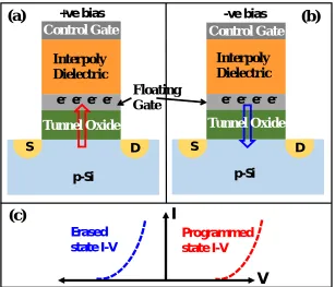
p - S i e - e - e - e
-S D
e - e - e - e
-I
V
E r a s e d
s t a t e I - V P r o g r a m m e d s t a t e I - V
+ v e b i a s - v e b i a s
( a )
( b )
( c )
p - S i
T u n n e l O x i d e
F l o a t i n g G a t e I n t e r p o l y
D i e l e c t r i c
C o n t r o l G a t e
I n t e r p o l y D i e l e c t r i c
T u n n e l O x i d e C o n t r o l G a t e
Figure 1.4: Operation of flash memory: (a) program operation, (b) erase operation, and (c) schematic of I-V curves of the memory after program and erase operation.
To read an SRAM cell, the bitlines (B and ¯B) are initially pre-charged to a high voltage level (or VDD). The word-line is then pulsed to VDD thereby turning ON the access transistors.
One of the bitline gets discharged through the inverter node of the cell storing logical 0. As a result, a differential voltage develops between the bitlines. This differential voltage is then sensed by a sense amplifier to detect the state of the cell. To write data in SRAM cell, the bitlines are initially driven to complementary voltage levels. The access transistors are then turned ON to write the data by providing bias at the wordline. The bitline which is kept at logical ”0” allows the corresponding inverter node to discharge through the access transistor. Similarly, the bitline kept at VDD charges-up the corresponding inverter node.
( a )
( b )
Figure 1.5: Schematic of flash arrangement in (a) NAND congifuration, and (b) NOR config-uration [15].
1.4
Flash memories
Flash memories are the core element of modern day SSDs [16]. These memories operate on the principle of storing electrons in a floating gate or charge-trap layer thereby realizing the programmed state of the device. These electrons can be taken back to the substrate with an erase operation. Figure 1.4 shows the device operation mechanisms of a typical floating gate type flash memory. The device consists of a transistor with a tunnel oxide, a floating gate serving as the charge storage layer, an interpoly dielectric (IPD) and a control gate. Instead of floating gate, a charge trap layer such as Nitride can also be used to store the electrons.
During programming, electrons are transferred from the substrate to the floating gate or nitride layer thereby increasing the threshold voltage of the transistor (shown in Figure 1.4 (a)). Similarly, an erase operation tunnels the electrons back to the substrate, thereby reducing the threshold voltage or VT (shown in Figure 1.4 (b)). Figure 1.4 (c) the schematic of drain current
considered to be binary-1 state, whereas erased state can be considered to be binary-0 state. With adequate control the number of electrons tunneled into the floating gate, intermediate states can be achieved, resulting in a multi-bit memory device. Once the charge is transferred into the floating gate, it should remain at the floating gate for 10 years, hence the tunnel oxide is chosen thick enough to prevent the charge loss after program operation. Similarly, to avoid the charge transfer between the control gate and the floating gate, very thick IPD are chosen. The flash cells can be arranged in either NAND or NOR configuration.
1.4.1 NAND flash
In NAND architecture, flash cells are connected in series, as shown in Figure 1.5 (a). During programming, a high +ve bias is applied to the wordline keeping the bitline grounded. The high bias at wordline (or at the control gate) results in a tunneling of electrons from the substrate to the floating gate. During erase, a high -ve bias is applied to the control gate which results in tunneling the electrons back to the substrate, as shown in Figure 1.4 (b). This operation reduces the VT of the transistor. Following are the key points about NAND flash:
Progam and erase operations are achieved with Fowler-Nordheim (FN) tunneling. Provids higher bit density than NOR.
cells are read sequentially, thus access time is much higher than NOR.
item Block erase: since all the cells share the same substrate, erase is achieved by applying bias at the substrate. NAND erase is faster than NOR.
Ideal usage: PC flash, secure digital media, flash drives, SSDs, etc.
Current NAND techology is based on 3D architecture where several layers of flash cells are arranged in a vertical trench [17]. Although this architecture provides significant area scaling advantage, but the scaling of flash memories rises several concerns. Figure 1.6 (a) show the NAND memory density trend [18]. The multi-level operation is achieved by setting different VT
levels with approrpiate control of number of electrons in the floating gate. With scaling, the number of electrons involved in flash operation has reduced significantly. Below 22 nm node, loss of just few electrons from the floating gate can change the VT by more than 100 mV. Thus,
loss of just few electrons can completely destroy the stored data.
1.4.2 NOR flash
(a) (b)
Figure 1.6: Trend of (a) NAND scaling, and (b) DRAM scaling [20].
accessed randomly making them attractive for fast memory applications. During programming, bias is applied to both bitline and wordline resulting in generation of hot electrons which gets injected into the floating gate. For this reason, the voltage requirement of NOR flash is lower than NAND cell. Schematic of NOR cell arrangement is shown in Figure 1.5 (b). Some of the key points of NOR flash are:
Progamming: Channel Hot Electron (CHE) injection is used. Erasing: achieved with Fowler-Nordheim (FN) tunneling.
Provides lower bit density because of metal connectivity required to source and drain of every transistor.
Provides random access, thus access time is lower than NAND.
Ideal usage: Code storage in PDAs and cell phones, embedded systems, etc.
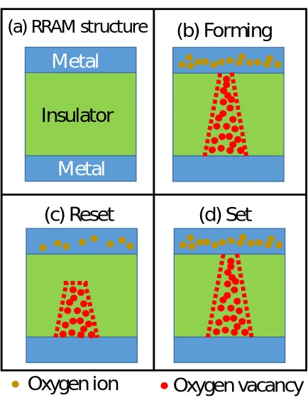
( b ) F o r m i n g
( c ) R e s e t
( d ) S e t
M e t a l
M e t a l
I n s u l a t o r
( a ) R R A M s t r u c t u r e
O x y g e n i o n
O x y g e n v a c a n c y
Figure 1.7: Schematic of RRAM and its operation; (a) device structure of RRAM, (b) forming operation, (c) reset operation and (d) set operation.
1.5
Resistive RAM (or RRAM)
RRAM has been attracting research interest for its tremendous potential for replacing the NAND cells for future memory technology. With the configuration of cross-bar array, they can achieve cell size lower than 4F2 thereby allowing aggressive area scaling possibilities. However, physical operation principles of these memories are still under research phase. Several models of operation has been proposed [21, 22, 23], but an accurate model to to describe different RRAM operations observed in different RRAM devices is still missing.
( a ) P C M d e v i c e
( b ) P C M o p e r a t i o n
T o p E l e c t r o d e
P h a s e c h a n g e m a t e r i a l
B o t t o m E l e c t r o d e
I n s u l a t o r
H e a t e r
P C
Figure 1.8: Schematic of (a) device structure of PCM, and (b) memory operation in PCM taken from [26].
operation which brings the insulator into high resistance state (HRS), shown in Figure 1.7 (c). Similarly, the ruptured part of the filament can be formed again with a set operation thereby bringing the LRS, shown in Figure 1.7 (d). Mode details of the RRAM and its operation are mentioned in Chapter-4 of the Dissertation.
1.6
Phase Change Memory (or PCM)
Figure 1.9: (a) Device structure of STT-MRAM, (b) HRS state of STT-MRAM and (c) LRS state of STT-MRAM [27].
set pulse allowing the chalcogenide to attain its crystalline state. Successive set and reset pulses are used to operate the PCM cell.
PCM has already been proposed to replace the flash in NOR architecture. Fast switching speed and excellent endurance behavior of PCM are also attractive for potential DRAM re-placement. However, the major concerns for PCM devices are higher cell size and inability to integrate in 3D stacks. More details of PCM devices can be found in [26].
1.7
Spin Transfer Torque Magnetic RAM (or STT-MRAM)
of a high current pulse. The high current passed from fixed layer into the free layer carries spin momentum which can switch the magnetization state of the free layer. Similarly, opposite polarity current pulse can reverse the magnetization state of the free layer. When two layers have similar magnetization states, the device attains its LRS state. On the other hand, if the layers have opposite magnetization states, this result in the HRS state of the device. Schematic representation of the HRS and LRS state of STT-MRAM are shown in Figure 1.9 (b) and Figure 1.9 (c).
Note that the materials used in STT-MRAM are ferromagnetic materials which are not compatible to the standard CMOS process. Moreover, a complete STT-MRAM device requires various metal layers to improve the ferromagnetic coupling and to fix the magnetization of the fixed layer. These are the prime concerns of the MRAM. Another concern of STT-MRAM is the requirement of very high current to switch the magnetization of the free layer. Thus, STT-MRAMs show high power memory operation. However, STT-MRAMs can be pro-grammed/erased within few tens of nanosecond, and they offer unlimited endurance (more than 1016). These two cruicial properties of STT-MRAM makes them the most suitable candidate
for DRAM replacement at present. More details of STT-MRAM can be found in [27].
1.8
Other emerging memory devices
The demand of meeting scaling laws in memory technology has resulted in several device con-cepts, both for DRAM and NAND replacement. Future research of all these emerging memory technologies is expected to result in a memory candidate that can satisfy all the criteria of a storage class memory [36].
Conductive Bridge RAM (or CBRAM) is very similar to the RRAM with an active elec-trolyte serving as the resistive switching layer, and the filamentary operation is controlled by an electrochemically active electrode and an inert electrode. One example is Pt/Ag2S/Ag where
the filament is formed in the Ag2S electrolyte [21]. Similarly, molecular electronics have also
1.9
Comparison of different memory technology
Emerging memory candidates seem to be promising in resolving some of the challenges faced by current flash and DRAM devices. PCM has been predicted to replace the flash memories in NOR cell below 45 nm node and below. RRAM provides very fast switching and cell size can be lower than 4F2. Thus, RRAM is expected to be a great competitor to NAND technology for non-volatile storage applications. STT-MRAM shows excellent endurance behavior with reasonable access time making them suitable for DRAM replacement. A comparison between all the promising memory technologies are presented in table 1.1 [33, 34, 35, 8].
Table 1.1: Comparison of different emerging memory technology candidates.
Parameter DRAM NAND RRAM PCM STT-MRAM
Cell Size (F2) 6-8 8 4 8-16 14-64
Write time 10-50 ns 0.1 ms 5-30 ns 20-30 ns 10 ns Write energy 0.005 pJ 100 pJ 1 pJ 6 pJ 4 pJ
Endurance 1016 105 1010 108 1015
Retention 64 ms 10 years 10 years 10 years weeks
3D capability via TSV Yes Yes No No
Process Complexity High High Low Low High
1.10
Dissertation overview
neuromor-phic systems, sensor systems. Unified memory can also result in significant reduction in circuit area (mitigating the requirement of TSV), as well as provide better security.
The primary requirement of a unified memory is to provide two basic needs, (i) a fast non-volatile storage element that can be used to store codes, and (ii) a low power, very fast memory that can behave like a DRAM for executing the logical operations. In this Dissertation, novel concepts of unified memory has been discussed and demonstrated.
Chapter-3 of the Dissertation discusses the concept of dual floating gate flash memory which can resemble a simultaneous volatile and non-volatile operation. The addition of an extra floating gate into the flash device has been observed to provide additional volatile memory functionality. A complete description of the theoretical insight of the memory operation has been discussed in this chapter. Unified memory operation from a fabricated device is also discussed in chapter-3. However, emerging memories such as RRAM provides lower cell size and faster switching speed compared to NAND technology. Thus, achieving a unified memory operation with RRAM devices can provide better performance than flash memories. For this purpose, this dissertation also covers unified memory operation that can be achieved with RRAM technology.
Since RRAM is a relatively new technology, a significant emphasis has been put to under-stand RRAM device operation principles. This consists of underunder-standing the non-volatile and volatile memory behavior of different RRAM candidates. Chapter-4 and chapter- 5 deals with the understanding of RRAM non-volatile operation. Understanding the forming operation of RRAM devices has been carried out in chapter-4 of the dissertation. A technique to reduce the forming voltage has also been explored in this chapter. Understanding of set and reset operation has been carried out in chapter-5 of the dissertation. A relation between abrupt and gradual reset with their corresponding set was observed which was further used to control the conduc-tance change in the dielectric with a novel technique. This technique was further used to realize analog memory behavior in binary oxide RRAMs applicable for neuromorphic computation systems.
1.11
Novel contributions
Chapter-3 of this dissertation describes about a dual floating gate unified memory MOSFET. This was the first demonstration of a transistor which can show simultaneous volatile and non-volatile operation. In the RRAM research, the technique of gradual filament dissolution has been adopted to implement synaptic learning. Such a gradual dissolution is a promising aspect of analog memory. The volatile memoryr behavior in RRAM has been used to realize a proof-of-concept 1T-0C ZRAM MOS capacitor device. In future work, the realization of 1T-0C ZRAM transistor can be a potential candidate for DRAM replacement.
1.12
Summary
REFERENCES
[1] International technology roadmap for semiconductors: Emerging Research Devices 2013, available online at www.itrs.net.
[2] H. Iwai, “Technology roadmap for 22nm and beyond,”International Workshop on Electron Devices and Semiconductor Technology (IEDST), pp. 1-4, 2009.
[3] S. E. Thompson, M. Armstrong, C. Auth, M. Alavi, M. Buehler, R. Chau, S. Cea, T. Ghani, G. Glass, T. Hoffman, C. H. Jan, C. Kenyon, J. Klaus, K. Kuhn, Z. Ma, B. Mcintyre, K. Mistry, A. Murthy, B. Obradovic, R. Nagisetty, P. Nguyen, S. Sivakumar, R. Shaheed, L. Shifren, B. Tufts, S. Tyagi, M. Bohr and Y. El-Mansy, “A 90-nm Logic Technology Featuring Strained-Silicon,” IEEE Transactions on Electron Devices, vol. 51, no. 11, pp. 1790-1797, 2004.
[4] C. Auth, A. Cappellani, J. S. Chun, A. Dalis, A. Davis, T. Ghani, G. Glass, T. Glassman, M. Harper, M. Hattendorf, P. Hentges, S. Jaloviar, S. Joshi, J. Klaus, K. Kuhn, D. Lavric, M. Lu, H. Mariappan, K. Mistry, B. Norris, N. Rahhal-orabi, P. Ranade, J. Sandford, L. Shifren, V. Souw, K. Tone, F. Tambwe, A. Thompson, D. Towner, T. Troeger, P. Vandervoorn, C. Wallace, J. Wiedemer and C Wiegand, “45nm High-k + metal gate strain-enhanced transistors,” IEEE Symposium on VLSI Technology pp.128-129, 2008.
[5] C. H. Jan, U. Bhattacharya, R. Brain, S. J. Choi, G. Curello, G. Gupta, W. Hafez, M. Jang, M. Kang, K. Komeyli, T. Leo, N. Nidhi, L. Pan, J. Park, K. Phoa, A. Rahman, C. Staus, H. Tashiro, C. Tsai, P. Vandervoorn, L. Yang, J. Y. Yeh and P. Bai, “A 22nm SoC Platform Technology Featuring 3-D Tri-Gate and High-k/Metal Gate, Optimized for Ultra Low Power, High Performance and High Density SoC Applications,” IEEE International Electron Device Meeting (IEDM), pp. 44-47, 2012.
Server Compute systems,” Flash Memory Summit, 2013.
[7] Y. Nishi, “Advances in Non- volatile Memory and Storage Technology,” Woodhead Pub-lishing Series in Electronic and Optical Materials: Number 64, 2014.
[8] G. S. Sandhu, “Emerging Memories Technology Landscape,” IEEE Non-Volatile Memory Technology Symposium (NVMTS), pp. 1-4, 2013.
[9] M. Koyanagi, “The Stacked Capacitor DRAM Cell and Three-Dimensional Memory,”IEEE Solid-State Circuits Society Newsletter, vol. 13, no. 1, pp. 37-41, 2008.
[10] E. Kultursay,M. Kandemir, A. Sivasubramaniam and O. Mutlu, “Evaluating STT-RAM as an Energy-Efficient Main Memory Alternative”, International Symposium on Performance Analysis of Systems and Software (ISPASS), pp. 256-267, 2013.
[11] B.C. Lee, E. Ipek, O. Mutlu and D. Burger, “Architecting phase change memory as a scalable DRAM alternative,” International Symposium on Computer Architecture (ISCA), pp. 2-13, 2009.
[12] A. Makarov, V. Sverdlov and S Selberherr, “New Trends in Microelectronics: Towards an Ultimate Memory Concept,” International Caribbean Conference on Devices, Circuts and Systems (ICCDCS), pp. 1-4, 2012.
[13] J. Singh, S. P. Mohanty and D. Pradhan, “Robust SRAM Designs and Analysis,”Springer Publications, 2013.
[14] C. Shin, “Advanced MOSFET Designs and Implications for SRAM Scaling”,Ph.D Thesis, University of California Berkeley, 2011.
[15] R. Micheloni, G. Campardo and P. Olivo, “Memories in Wireless Systems,”Springer Pub-lications, 2008.
[17] A. Goda, “Opportunities and challenges of 3D NAND scaling,” International Symposium on VLSI Technology, Systems, and Applications (VLSI-TSA), pp. 1-2, 2013.
[18] ISSCC Technology Trend,International Solid-State Circuits Conference (ISSCC), 2014.
[19] J. H. Yoon and G. A. Tressler, “Advanced flash technology status, scaling trends and implications to enterprise SSD technology enablement,” Flash memory summit, 2012.
[20] S. K. Park, “Technology Scaling Challenge and Future Prospects of DRAM and NAND Flash Memory,” IEEE International Memory Workshop (IMW), pp. 1-4, 2015.
[21] K. M. Kim, D. S. Jeong and C. S. Hwang, “Nanofilamentary resistive switching in binary oxide system; a review on the present status and outlook,”Nanotechnology, vol. 22, 254002, 2011.
[22] J. J. Yang, D.B. Strukov and D. R. Stewart, “Memristive Devices for Computing,”Nature Nanotechnology, vol. 8, pp. 13-24, 2013.
[23] R. Waser, “Resistive non-volatile memory devices (Invited Paper),”Microelectronic Engi-neering, vol. 86, pp. 19251928 , 2009.
[24] C. B. Lee, B. S. Kang, A. Benayad, M. J. Lee and S. E. Ahn, “Effects of metal electrodes on the resistive memory switching property of NiO thin films,” Applied Physics Letters, vol. 93, 042115, 2008.
[25] A. Prakash, J. Park, J. Song, J. Woo, E. J. Cha and H. Hwang, “Demonstration of Low Power 3-bit Multilevel Cell Characteristics in a TaOx-Based RRAM by Stack Engineering,” IEEE Electron Device Letters, vol. 36, no. 1, pp. 32-34, 2015.
[27] K. L. Wang, J. G. Alzate and P. K. Amiri, “Low-power non-volatile spintronic memory: STT-RAM and beyond,” Journal of Physics D: Applied Physics, vol. 46, 074003, 2013.
[28] B. Radha, A. A. Sagade and G. U. Kulkarni, “Metal-organic molecular device for non-volatile memory storage,” Applied Physics Letters, vol. 105, 083103, 2014.
[29] C. M. Lin, W. Shih, I. Y. Chang, P. C. Juan and J. Y. Lee, “Metal-ferroelectric ( BiFeO3 ) -insulator (Y2O3) -semiconductor capacitors and field effect transistors for nonvolatile memory applications,” Applied Physics Letters, vol. 94, 142905, 2009.
[30] J. W.Seo, J. W. Park, K. S. Lim, S. J. Kang, Y. H. Hong, J. H. Yang, L. Fang, G. Y. Sang and H. K. Kim, “Transparent flexible resistive random access memory fabricated at room temperature,”Applied Physics Letters, vol. 95, 133508, 2009.
[31] W. W. Jang, J. O. Lee, H. H. Yang, and J. B. Yoon, “Mechanically Operated Random Access Memory (MORAM) Based on an Electrostatic Microswitch for Nonvolatile Memory Applications,”IEEE Transactions on Electron Devices, vol. 55, no. 10, pp. 2785-2789, 2008.
[32] J. S. Meena, S. M.Sze, U. Chand and T. Y. Tseng, “Overview of emerging nonvolatile memory technologies,” Nanoscale Research Letters, vol. 9, 526, 2014.
[33] M. Marinella, “The Future of Memory,” IEEE Aerospace Conference, pp. 1-11, 2013.
[34] D. S. Jeong, R. Thomas, R. S. Katiyar, J. F. Scott, H. Kohlstedt, A. Petraru and C. S. Hwang, “Emerging memories: resistive switching mechanisms and current status,” Reports On Progress in Physics, vol. 75, 076502, 2012.
[35] A. Chen, J. Hutchby, V. Zhirnov and G. Bourianoff, “Emerging Nanoelectronic Devices,” John Wiley and Sons Ltd, 2014.
Chapter 2
Experimental Methods
This dissertation accounts for fabrication and characterization of DFGFET and RRAM devices. The fabrication process flow of these devices is mentioned in Appendix-A. Standard CMOS process such as deposition, etching, lithography, etc, were used for fabrication of the devices. Details of the individual unit process can be found in [1]. Characterization of the devices was performed by either electrical characterization systems or physical characterization systems. Electrical characterization was performed with keithley 4200 SCS parameter analyzer [2], HP 4155B semiconductor parameter analyzer [3] and Agilent E-4980A LCR meter [4]. Physical characterization was performed using systems like XRD and XPS.
2.1
Primary fabrication tools used
Description of some of the tools primarily used for device fabrication is mentioned below.
2.1.1 Atomic layer deposition
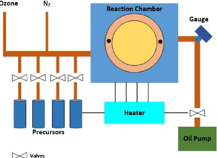
Atomic layer deposition (or ALD) is highly used to deposit dielectric and metals with precise thickness control [5]. In this work, ALD process has been used to deposit dielectric films. For this purpose, a commercial Savannah S100 ALD system from Cambridge Nanotech was used [6]. Schematic of the ALD system is shown in Figure 2.1. The tool is equipped with high speed pneumatic valves in order to precisely control the pulse time (in a range of ms) of precursors. Two heater lines were connected to the substrate holder supporting temperature range up to 400◦C.
Figure 2.1: Schematic of ALD system.
great conformality. Another advantage of ALD is the low temperature deposition process which is highly used in flexible/transparent electronics. However, the deposition temperature should be kept at higher than the minimum required temperature for the reaction to occur on the substrate surface. Too low deposition temperature results in a thermally activated chemisorption as well as decrease in the deposition rate. On the other hand, if the deposition temperature is too high, chemical bonding cannot be sustained or the density of chemically reactive sites is reduced.
Figure 2.1 shows the schematic of the ALD chamber used in this dissertation work. The samples are kept in the reaction chamber which is connected to several precursor cylinders as well as carrier gas N2. All the precursors have high speed valves which can be opened and closed
The dielectric deposition process involves the repeated cyclic execution of four critical steps: The metalorganic precursor is served in the ALD chamber by an inert carrier gas like N2. Precursor molecules get chemisorbed on the hydroxylated/oxidized surfaces of the
substrate. ALD is a self-limited reaction which stops once the entire surface is saturated by the precursor molecules.
The unreacted precursor molecules are purged out of the chamber through a pump.
Next, the oxidizing precursor such as water or ozone is sent into the chamber to oxidize the new surface and eliminate the organic ligand as a gaseous by-product.
The unreacted precursor and the gaseous by-products are then purged out of the chamber through the pump.
Table 2.1: Different ALD recipe.
Dielectric Precursors Temperature
Al2O3 Tri-methyl Aluminium (TMA) + H2O 200◦C
HfO2 Tetrakis-dimethyl-amino-hafnium (TDMAH) + H2O 200◦C
SiO2 3-amino-propyl-triethoxy-silane (APTS) + H2O + O3 150◦C
TiO2 tetrakis(dimethylamino) titanium (TDMAT) + H2O 200◦C
Table 2.1 shows the typical recipe for ALD used for different parts of the dissertation work [7]. In many cases, multiple oxidizing chemistries may be required to ensure completeness of the oxidizing step (e.g. both water and ozone are required for SiO2 deposition). Also, an
optimization of the ALD process recipe is required to ensure sufficient precursor quantity and reaction time for each precursor step. This may also require heating the precursor cylinder to increase the vapor pressure. Details of the specific precursors and the recipe conditions used for different ALD dielectrics are provided in Table 2.1. Note that compound dielectric like HfAlO was deposited with repeated cycles of HfO2 followed Al2O3 cycle.
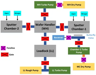
2.1.2 UHV RF magnetron sputtering
Loadlock (LL)
Wafer Handler
(WH)
Sputter
Chamber-1
Sputter
Chamber-2
LL Rough Pump LL Turbo Pump
Chamber-1 Turbo Pump WH Turbo Pump
Baratron
Butterfly Valve
MC Dry Pump
Argon Nitrogen Argon Nitrogen
WH Dry Pump
Foreline
Gate
Figure 2.2: Schematic of UHV-RF sputter system.
substrate is kept at ground potential. When the plasma of inert gas like Argon is introduced in the chamber, positively charged Ar ions accelerates to the negatively charged target material. Since these energetic positively charged ions eject target atoms through the energy transfer. The ejected atoms then get deposited on the substrate.
A magnetic field can be used to enhance sputtering yield. The magnetic field is applied by using a magnetron behind the target material. The magnetron creates a magnetic field that increases the density of plasma near the target resulting in a higher deposition rate at a lower input power. Radio-Frequency (RF) sputtering is also used to deposit dielectric materials. During RF sputtering, electron oscillation with ac field results in no charge accumulation at the target surface.
Provides high deposition rate.
Provides capability to deposit complex alloys.
Allows deposition of most of the metals as well as dielectrics.
All the metal electrodes used in this dissertation work were deposited using UHV RF mag-netron sputtering system. Schematic of the UHV-RF sputtering system is shown in Figure 2.2. Details about RF sputtering mechanism can be found in [9]. The base pressure of main chamber was kept lower than 1 x 10⁻⁷ Torr in order to minimize the level of impurities in the chamber. Three RF-magnetron guns are attached on top of the each sputtering chamber. Thus, a total of six different materials or metal alloys can be easily deposited without breaking the vacuum. For reactive sputtering of metal like TaN, deposition was done by flowing Ar andN2simultaneously.
The deposition pressure was set to 5 mTorr after the gas flow in order to prevent gas-phase collision and optimized deposition rate. More details on the sputtering system can be found in [14].
2.2
Analytical characterization methods
Analytical methods are useful in order to understand the physical properties of different mate-rials. Some of the essential physical properties are atomic structure of the material, crystallinity of the material etc. Following techniques were used to characterize different dielectric used in this dissertation.
2.2.1 X-ray photoelectron spectroscopy
X-Ray Photoelectron Spectroscopy (XPS) is highly used to analyze the chemical information in ultrathin high-k oxides or at the surface [10]. After depositing thin films, XPS is used to find the presence of the desired material, along with traces of contaminants as well as defects like oxygen vacancies. During XPS measurement, x-rays are illuminated on the substrate, and electrons ejected from the substrate material is analyzed to find out chemical information.
Figure 2.3: Schematic of the X-ray photoelectron spectroscopy method.
Consider the incident x-ray have an energy of hν, then the energy relation is expressed as:
hν=KE+BE (2.1)
whereBE is the binding energy of the electron. Sinceν of the x-rays are a known quantity, and the quantity hν is the photon energy. Subtracting the KE of the ejected electrons from the photon energy results in the binding energy of the material under observation. This binding energy can reveal many important information about the material. If the binding energy is low, it means the electrons in the orbital are far away from the nucleus, and vice versa. The exact binding energy can be used to determine the orbital of the electrons thereby estimating the entire electronic configuration. This technique can also be used to complex materials such as dielectrics, alloys etc. Details about XPS analysis can be found in [11].
In this dissertation, XPS analysis has been used to determine the electronic configuration of TiO2 dielectric, mentioned in chapter-6. The volatile operation using RRAM requires the
Figure 2.4: Schematic of the X-ray diffraction method.
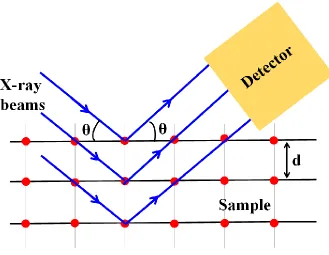
2.2.2 X-ray diffraction analysis
X-ray diffraction (or XRD) analysis is performed to analyze if a material is in crystalline, poly-crystalline or amorphous form [12]. During XRD, x-rays at different incident angle are injected into the material and the reflected x-ray is analyzed by a detector, as shown in Figure 2.4. Only short wavelength x-rays (in the range of a few angstroms) are used so that the wavelength of x-rays is comparable to the size of atoms in the sample under observation. Commonly, Cu and Mo are used as the x-ray source which emits 8 keV and 14 keV x-rays with corresponding wavelengths of 1.54 and 0.8 respectively. The energetic x-rays can penetrate into the materials under observation, and provide desired information about the material.
The x-ray have known characteristic wavelength (say λ ). When they are thrown on a sample, they get reflected and the reflected spectra is analyzed by a detector to determine the crystalline state of the material. Consider the rays fall on the sample at an angle θ, then the Bragg’s law can be written as:
where d is the inter-atomic distance in the material. If the material is crystalline, and the distance between the atoms are integral multiple ofλ, then the x-ray received at the detector will have a constructive interference at certain angleθthereby resulting in a peak in the received signal. On the other hand, amorphous materials will have only the destructive interference of the x-rays at the detectors, hence no peaks will be observed. Depending upon the location of peaks along the θ axis (usually 2θ is used for convenience), one can determine the materials in the sample as well as its crystal information. Similarly, in poly-crystalline materials, several peaks are observed in the XRD analysis. Hence XRD is a useful tool to extract the crystallographic information of the material.
In this dissertation, XRD has been used to determine crystalinity of TiO2 dielectric
de-posited using ALD system. To understand the volatile operation in non-filamentary RRAM, it is important to analyze the crystallographic properties of the RRAM dielectric. Results of TiO2
XRD measurement is mentioned in chapter-6 of the dissertation.
2.3
Electrical characterization methods
Electrical characterization methods has been extensively used in this dissertation work. Elec-trical characterization provides the information of device behavior such as current-voltage re-lationship, capacitance-voltage rere-lationship, etc. Electrical characterization of semiconductor devices is a vast area, with several techniques used to understand different device behavior. A detailed analysis of most of the electrical characterization techniques used in modern day semiconductor electronics can be found in [15].
2.3.1 Capacitance-Voltage measurements
Capacitance-Voltage (or CV) measurements are highly used to characterize MOS capacitors in order to find parameters like dielectric constant, flatband voltage, threshold voltage etc. Figure 2.5 shows the typical CV characteristics of a MOS capacitor fabricated on p-Si substrate [13]. At -ve bias voltages, the holes at the substrate accumulates near the interface, and this mode is called the accumulation mode. At this mode, the capacitance is referred at Cmax, which
is the capacitance corresponding to the equivalent oxide thickness.
As the voltage goes toward +ve bias, holes are repelled from the Si/SiO2 interface gradually
making the depletion mode. At certain bias, all the bands are flat, and the voltage at which this condition is met is termed as flatband voltage (VF B). A maximum width of depletion
Figure 2.5: (a) Band diagram of MOS capacitor and (b) CV analysis of MOS capacitor.
frequency CV (or LFCV) analysis. This is called threshold point where the inversion charge starts appearing in the LFCV curve of the MOS capacitor. The capacitance just before inversion is Cmin, and it goes back to Cmax after the inversion point. At high frequency (HFCV), the
carriers don’t get enough time to respond to the signal, hence capacitance remains at Cmin in
the inversion region.
2.3.2 Currrent-Voltage measurements of DFGFET
Current-voltage (or IV) measurements are used to understand the transistor behavior and sev-eral current conduction mechanisms. For understanding the dual floating gate memory MOSS-FET device, 4-terminal IV measurements were performed to find the VT of the transistor.
Figure 2.6 shows the typical linear ID-VG characteristics of MOSFET. For extracting the VT,
transconductance is calculated from the ID-VG curve and plotted against the voltage. At the
peak of the transconductance point, a line is drawn which intersects the ID-VG curve. At the
Figure 2.6: Typical ID-VG characteristics of MOSFET and extraction of VT.
All the non-volatile performance analysis of the dual floating gate memory MOSFET was carried out with VT analysis of the transistor. Key points of electrical characterization of dual
floating gate MOSFET are mentioned below:
To measure the non-volatile program and erase window: VT of the MOSFET was
mea-sured to analyze the programming or erasing behavior. During program window analysis, VT of selected virgin devices were measured, followed by VT measurement after every
pro-gramming pulse applied. While during erase, the devices were initially taken into program state followed by successive erasing operations.
Non-volatile retention measurement: Devices were taken into program and erase state, and VT was monitored for different time intervals.
Non-volatile endurance measurement: A single device was initially selected, and VT of
the device was measured after program and erase operation. Repeated program and erase cycles were then applied to the device, and the VT of the device was measured after
specific different cycle numbers.
scheme. In this measurement, the program and read pulses were applied, and the ca-pacitance of the gate stack was monitored. The details are mentioned in chapter-3.
2.3.3 Currrent-Voltage measurements of RRAM
Unlike floating gate memory devices, RRAMs are two terminal devices. Hence the 2-terminal IV measurement for resistor was used to study the RRAMs. In this measurement setup, one terminal of the resistor is grounded, and bias is applied to the other terminal. Key points of measuring RRAM behavior are mentioned below:
Forming operation: Forming operations were performed by applying bias at one of the selected electrode keeping the other electrode grounded. To prevent the devices going into hard breakdown, the current through the terminals were limited to a compliance limit.
Reset operation: All the RRAM devices mentioned in this thesis were observed to show bipolar RRAM operation. During reset, negative bias was applied to the desired electrode keeping the other electrode grounded. No compliance limit is required during reset.
Set operation: set operation is very similar to the forming operation. The only difference between set operation and forming operation is the voltage window. Since forming refers to the creation of the filament in the dielectric which can connect two electrode, a high bias is desired during forming operation. Set operation, on the other hand, requires to just re-create the broken filament. Hence the set voltage is lower than forming voltage.
Synaptic learning: synaptic learning operation mentioned in chapter-5 of the thesis were performed with set and reset pulses. After every set and reset pulses, read pulses were applied to measure the conductance of the dielectric.
Volatile RRAM operation: Since the volatile RRAM operation was measured on a SiO2/TiO2
MOS capacitor, pulsed-CV scheme was used to monitor the capacitance. Program pulses were applied to the gate of the MOS capacitor, and the capacitance change was measured with successive read pulses.
2.4
Summary
REFERENCES
[1] J. D. Plummer, M. D. Deal and P. B. Griffin, “Silicon VLSI Technology: Fundamentals, Practice and Modeling,” Prentice Hall publication, 2000.
[2] Keithley 4200-SCS Parameter Analyzer,
www.keithley.com/products/semiconductor/parametricanalyzer/dcac/currentvoltage/4200scs
[3] 4155B / 4156B Semiconductor Parameter Analyzers, www.keysight.com/en/pd-542813-pn-4155B/semiconductor-parameter-analyzers
[4] E4980A Precision LCR Meter, www.keysight.com/en/pd-715495-pn-E4980A/precision-lcr-meter-20-hz-to-2-mhz
[5] N. Pinna and M. Knez, “Atomic Layer Deposition of Nanostructured Materials,” Wiley-VCH publication, 2011.
[6] Ultratech/Cambridge NanoTech Simply ALD, http://www.cambridgenanotechald.com/atomic-layer-deposition.shtml.
[7] N. Ramanan, “Investigation of ALD Dielectrics for Improved Threshold Voltage Stabil-ity and Current Collapse Suppression in AlGaN/GaN MOS-HFETs,” Ph.D Thesis, North Carolina State University, 2014.
[8] S. Franssila, “Introduction to Microfabrication, 2nd edition” Wiley publication, 2010.
[9] Y. W. Chung, “Introduction to Materials Science and Engineering,”CRC Press, 2006.
[10] S. Iwata and A. Ishizaka, “Electron spectroscopic analysis of the Si/SiO2 system and corre-lation with metal-oxide-semiconductor device characteristics,” Journal of Applied Physics, vol. 79, pp. 6653-6709, 1996.
[12] Y. Waseda, E. Matsubara and K. Shinoda, “X-Ray Diffraction Crystallography,”Springer Berlin Heidelberg publication, 2011.
[13] Y. Taur and T. H. Ning, “Fundamentals of Modern VLSI Devices,”Cambridge University Press, 2009.
[14] B. Lee, “A Study of Group III Elements (La, Gd, Eu, and Al) Incorporation on Metal Gate / Highk Stacks for Advanced CMOS Applications,” Ph.D Thesis, North Carolina State University, 2010.
Chapter 3
Dual Floating Gate Memory
MOSFET
Modern smart electronic devices rely extensively on volatile and non-volatile memories. While codes and look-up tables are stored in the non-volatile memory, the logical operations are per-formed using the volatile memories [1]. The processing unit has separate area on chip dedicated to the non-volatile storage and the volatile memories. Random Operating Memory (ROM) and non-volatile memories serve as the storage section of the processor, whereas volatile memories like DRAM and SRAM are highly used for execution along with other logic circuits. Flash memories serve as the core device of NAND and NOR non-volatile memory array [2].
Among NAND and NOR, NOR is usually preferred to store codes because of their faster access time [3]. Traditionally, nitride based charge trap layer is used to store the charge in the oxide. Charge trap flash memories (like SONOS and TANOS flash memories) have been studied extensively to meet P/E window requirements, good retention and endurance characteristics [4, 5, 6, 7]. All these devices have their own advantages and disadvantages. A thorough under-standing of these devices have resulted in tremendous memory capacity in solid state drives and flash drives. Similarly, DRAM and SRAM have also been a major components of electronic processor. DRAMs are necessary to process data and make logical operations, whereas SRAMs are used as cache memory. 1T-1C DRAM has been the preferred DRAM choice, but several new DRAM technologies which employs 1T-0C configuration have been proposed to improve DRAM performance [8, 9]. Similarly, different SRAM architectures have also been proposed to meet the scaling needs [10].
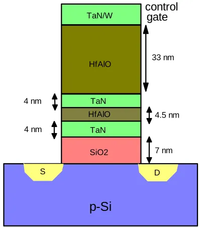
7 n m S i O 2
T a N H f A l O
T a N H f A l O T a N / W
4 . 5 n m 3 3 n m
4 n m
4 n m
S D
c o n t r o l g a t e
p - S i
Figure 3.1: Schematic representation of the dual floating gate memory MOSFET.
speed, provide better security and area efficient solutions. 3D vertical stacking using through silicon via (TSV) technology seems to be a promising idea to meet this requirement [12, 13]. Although independent improvement of DRAM and flash memory can meet future power require-ments, a significant improvement in power consumption can be obtained if both technologies are combined into a single transistor [14]. A unified memory which can simultaneously operate in volatile and non-volatile regime can also help to create a simpler computational architecture that occupies a lesser circuit area [18].
3.1
Theoretical understanding of the dual floating gate memory
MOSFET
The schematic representation of the dual floating gate memory MOSFET (or DFGFET) is shown in Figure 3.1. The transistor consists of following gate stack: tunnel oxide (TO), bot-tom floating gate (BFG), intermediate dielectric (IMD) which separates the floating gates, top floating gate (TFG), inter-poly dielectric (IPD) and control gate (CG). Detailed fabrication process flow can be found in Appendix-A. The purpose of keeping TO, BFG and IPD are sim-ilar to that of flash memory. However, an additional floating gate (TFG) and a thin dielectric (IMD) provides additional functionality to the flash memory. The device operation principles are discussed in subsequent sections.
3.1.1 Device operation
Figure 3.2 shows the band-diagram description of the device. Non-volatile operation is realized with charge transfer between the channel and the floating gates, whereas the volatile operation is performed with a charge transfer between the floating gates. A very high voltage at CG will result in charge transfer between the floating gates and the substrate with the help of Fowler-Nordheim (FN) Tunneling. This transition results in a significant increase in the threshold voltage (or VT). Similarly, a very high negative bias at the CG will move back the electrons
from the floating gates to the substrate thereby decreasing the VT significantly. These two
operations are very similar to the non-volatile operations in conventional flash memories. The increasedVT state is referred as the non-volatile programmed state, whereas the decreased VT
state is referred as non-volatile erase state.
However, with a relatively smaller bias at the CG, charge can be moved within the floating gates with the help of direct tunneling thereby making a relatively smaller threshold voltage (or VT) shift in the device. To enable this criteria, the EOT of the dielectric (IMD) separating the
B F G T F G C G
P r o g r a m
E r a s e
P r o g r a m
E r a s e
N o n - v o l a t i l e o p e r a t i o n
D y n a m i c o p e r a t i o n
p - S i
T O X I M D I P D
Figure 3.2: Band diagram representation of the operation modes in DFGFET.
Most attractive feature of the device is the concurrent mode of operation where the device can be used simultaneously for volatile and volatile mode operation. Let’s assume the non-volatile operation with a high positive bias at CG broughtK electrons into the floating gates from the substrate. After a reasonable time, these charges will balance themselves between the floating gates, sayK/2 electrons are stored in BFG andK/2 electrons in TFG. The VT at this
condition corresponds to the non-volatile programmed state. Now a relatively smaller bias at CG can move K/4 electrons from BFG into TFG, leaving behind K/4 electrons at the BFG and 3K/4 electrons in the TFG. VT at this condition will be different from the non-volatile VT.
This corresponds to the concurrent mode of operation (non-volatile programmed state, volatile programmed state). A similar operation can be performed after non-volatile erase operation. Hence the device can potentially store 2-bits at a VT location, one bit corresponding to the
non-volatile operation (programmed or erased), and the other bit corresponding to the volatile bit.
3.1.2 Theoretical formulation
A better understanding of the device working can be obtained by formulating the device opera-tions. Consider the structure shown in Figure 3.1. It is known that the flat-band voltage (VF B)
and VT of a transistor is highly dependent on the trapped charge in the dielectric. Floating
![Figure 1.5:Schematic of flash arrangement in (a) NAND congifuration, and (b) NOR config-uration [15].](https://thumb-us.123doks.com/thumbv2/123dok_us/1235860.1156109/21.612.101.528.76.367/figure-schematic-ash-arrangement-nand-congifuration-cong-uration.webp)
![Figure 1.8:Schematic of (a) device structure of PCM, and (b) memory operation in PCMtaken from [26].](https://thumb-us.123doks.com/thumbv2/123dok_us/1235860.1156109/25.612.138.493.74.331/figure-schematic-device-structure-pcm-memory-operation-pcmtaken.webp)
![Figure 1.9:(a) Device structure of STT-MRAM, (b) HRS state of STT-MRAM and (c) LRSstate of STT-MRAM [27].](https://thumb-us.123doks.com/thumbv2/123dok_us/1235860.1156109/26.612.145.487.78.344/figure-device-structure-mram-state-mram-lrsstate-mram.webp)